EP1512214B2 - Bobine a compensation de courant et circuit comprenant cette bobine a compensation de courant - Google Patents
Bobine a compensation de courant et circuit comprenant cette bobine a compensation de courant Download PDFInfo
- Publication number
- EP1512214B2 EP1512214B2 EP03737935.1A EP03737935A EP1512214B2 EP 1512214 B2 EP1512214 B2 EP 1512214B2 EP 03737935 A EP03737935 A EP 03737935A EP 1512214 B2 EP1512214 B2 EP 1512214B2
- Authority
- EP
- European Patent Office
- Prior art keywords
- current
- choke
- core
- auxiliary winding
- input
- Prior art date
- Legal status (The legal status is an assumption and is not a legal conclusion. Google has not performed a legal analysis and makes no representation as to the accuracy of the status listed.)
- Expired - Lifetime
Links
Images


Classifications
-
- H—ELECTRICITY
- H02—GENERATION; CONVERSION OR DISTRIBUTION OF ELECTRIC POWER
- H02J—ELECTRIC POWER NETWORKS; CIRCUIT ARRANGEMENTS OR SYSTEMS FOR SUPPLYING OR DISTRIBUTING ELECTRIC POWER; SYSTEMS FOR STORING ELECTRIC ENERGY
- H02J3/00—Circuit arrangements for AC mains or AC distribution networks
- H02J3/01—Arrangements for reducing harmonics or ripples
-
- H—ELECTRICITY
- H01—ELECTRIC ELEMENTS
- H01F—MAGNETS; INDUCTANCES; TRANSFORMERS; SELECTION OF MATERIALS FOR THEIR MAGNETIC PROPERTIES
- H01F27/00—Details of transformers or inductances, in general
- H01F27/34—Special means for preventing or reducing unwanted electric or magnetic effects, e.g. no-load losses, reactive currents, harmonics, oscillations, leakage fields
- H01F27/38—Auxiliary core members; Auxiliary coils or windings
-
- H—ELECTRICITY
- H02—GENERATION; CONVERSION OR DISTRIBUTION OF ELECTRIC POWER
- H02M—APPARATUS FOR CONVERSION BETWEEN AC AND AC, BETWEEN AC AND DC, OR BETWEEN DC AND DC, AND FOR USE WITH MAINS OR SIMILAR POWER SUPPLY SYSTEMS; CONVERSION OF DC OR AC INPUT POWER INTO SURGE OUTPUT POWER; CONTROL OR REGULATION THEREOF
- H02M1/00—Details of apparatus for conversion
- H02M1/12—Arrangements for reducing harmonics from AC input or output
- H02M1/126—Arrangements for reducing harmonics from AC input or output using passive filters
-
- Y—GENERAL TAGGING OF NEW TECHNOLOGICAL DEVELOPMENTS; GENERAL TAGGING OF CROSS-SECTIONAL TECHNOLOGIES SPANNING OVER SEVERAL SECTIONS OF THE IPC; TECHNICAL SUBJECTS COVERED BY FORMER USPC CROSS-REFERENCE ART COLLECTIONS [XRACs] AND DIGESTS
- Y02—TECHNOLOGIES OR APPLICATIONS FOR MITIGATION OR ADAPTATION AGAINST CLIMATE CHANGE
- Y02E—REDUCTION OF GREENHOUSE GAS [GHG] EMISSIONS, RELATED TO ENERGY GENERATION, TRANSMISSION OR DISTRIBUTION
- Y02E40/00—Technologies for an efficient electrical power generation, transmission or distribution
- Y02E40/40—Arrangements for reducing harmonics
Definitions
- the invention relates to a current-compensated choke having at least two windings which are arranged on a common core and each have an input and an output, and an additional auxiliary winding which has an input and an output.
- Common mode chokes are typically connected between a grid and an electrical device powered by the grid. These chokes are intended to reduce radio interference from the device to the network.
- Current-compensated chokes of the type mentioned above are preferably used for damping asymmetric interference currents that could be fed into the supply network by a frequency converter, for example.
- every device connected to a supply network has repercussions on the supply network. In the case of high-frequency repercussions, one speaks of radio interference.
- a current-compensated choke of the type mentioned is known, in which an electrical resistance is connected between the input and the output of the auxiliary winding.
- the purpose of the auxiliary winding is to reduce asymmetrical currents by transforming the resistor connected to the terminals of the auxiliary winding into the path of the asymmetrical interference current with the square of the transformation ratio. Coupling the resistor into the asymmetrical current path prevents the asymmetrical interference current from rising to excessively high values and thus prevents the choke core from being saturated.
- the resistor is not only loaded by current peaks, but constantly and must be designed for correspondingly high loads.
- the inductance of the choke is reduced even in the case of small asymmetrical currents, for which saturation of the core is not yet a problem, as a result of which the interference suppression effect of the choke is impaired.
- the effect of the auxiliary winding is also independent of the frequency used, so that the resistor must also absorb the power loss generated by interference currents, which occur in a frequency range where they do not exceed critical values.
- the aim of the present invention is therefore to provide a circuit arrangement with a choke of the type mentioned at the outset, which has an improved interference suppression effect.
- the invention specifies a circuit arrangement with a current-compensated choke, which has at least two windings which are arranged on a common core and each have an input and an output. Furthermore, the choke according to the invention has an additional auxiliary winding which is arranged on the core of the choke and which has an input and an output.
- a special winding direction is not required. It is easiest if all windings, including the auxiliary winding, are applied to the core in the same direction. However, the windings could also be applied in opposite directions.
- a changing impedance is connected between the input and the output of the auxiliary winding, the value of which changes as a result of influencing factors such as interference current or frequency.
- the asymmetrical interference current generates a magnetic flux in the core of the choke according to the invention. This causes a current to flow in the auxiliary winding and thus also through the impedance connected to the auxiliary winding.
- the value of this impedance changes in contrast to that of DE 295 06 951 U1 already known choke, depending on the current flowing through it and / or its frequency. This impedance is in turn transformed with the square of the transformation ratio into the path of the interference current.
- the changing impedance can be chosen to be small for low currents and large for high currents. This results in the advantage for the choke according to the invention that the inductance of the choke is not yet reduced in the case of small asymmetrical currents, as a result of which the interference suppression effect is improved.
- the changing impedance can also be made to change as a function of frequency.
- variable impedance can be a series resonant circuit made up of a capacitance and an inductance.
- a series resonant circuit made up of a capacitance and an inductance has a very low impedance at a frequency f 0 given by the values of the capacitance or inductance, as a result of which saturation of the inductor becomes effective particularly at frequency f 0 or close to frequency f 0 can be reduced.
- the changing impedance is a parallel resonant circuit made up of a capacitance and an inductance.
- a parallel resonant circuit made up of a capacitance and an inductance has a high impedance at a frequency f 0 given by the capacitance and the inductance.
- the inductance is a winding with its own core
- the examples mentioned for parallel or series resonant circuits made up of capacitance and inductance also produce a load-dependent behavior of the circuit connected to the auxiliary winding.
- the changing impedance is an active device that is controllable.
- a transistor for example, can be considered as such an active component, the emitter-collector path of the transistor being connected in series with a resistor between the input and output of the auxiliary winding.
- Such a transistor can, for example, be controlled on the base side by means of a controller that compares an asymmetrical interference value measured on the lines leading to the choke with a desired setpoint value, and correspondingly controls the emitter-collector path of the transistor via the base and thus generates a Control-controlled influence of the auxiliary winding exerts on the choke.
- the inputs of the windings of the current-compensated choke are connected to the phases or the neutral conductor of a network and the outputs of the windings are connected to a source of radio interference.
- Such a circuit arrangement has the advantage that due to the current-compensated choke according to the invention, whose auxiliary winding is connected to a changing impedance, an effective decoupling of the interference generated by the source of radio interference from the network, depending on the frequency, for example, can be achieved.
- FIG 1 shows a current-compensated choke according to the invention with windings W 1 , W 2 , W 3 .
- the windings W 1 , W 2 , W 3 are wound on a common core 1 .
- a core 1 can be a toroidal core, for example.
- the use of core materials with high permeability has a particularly advantageous effect here.
- Each of the windings W 1 , W 2 , W 3 has an input E1 , E2 , E3 and an output A 1 , A 2 , A 3 .
- the current-compensated choke has an auxiliary circuit 7, which includes an auxiliary winding W H .
- the auxiliary winding W H is wound on the common core 1 of the choke. It has an input E H and an output A H .
- a changing impedance Z is connected between the input E H and the output A H .
- the windings W 1 , W 2 , W 3 are wound in such a way that a symmetrical current through the choke causes only a negligible induction in the core 1 .
- the auxiliary winding W H it is irrelevant how the direction of winding is selected.
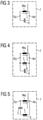
- the changing impedance is a parallel resonant circuit of an inductance L with its own core 8 and a capacitance C.
- the changing impedance is a series resonant circuit made up of a capacitance C and an inductance L.
- the inductance L according to figure 5 can be designed, for example, as a coil with its own core 8, whereby a behavior dependent on the current through the choke or on the current through the auxiliary winding W H behavior of the auxiliary winding W H can be generated.
- FIG figure 6 shows as a further example an auxiliary circuit 7 for use in an arrangement according to FIG figure 1 , in which the variable impedance is a series connection of a resistor R and the emitter-collector path of a transistor T.
- the transistor T can be driven on the base side by a controller 4 which compares an actual value 5 with a desired value 6 and sets the resistance of the emitter-collector path of the transistor T to a suitable value 5 .
- the actual value 5 can be, for example, the asymmetric interference measured at the inductor.
- the desired value 6 can be, for example, the optimal saturation of the inductor that can be set with the aid of the auxiliary winding W H .
- figure 7 shows a circuit arrangement with a current-compensated choke according to the invention according to FIG figure 1 , wherein the inputs E 1 , E 2 , E 3 of the windings W 1 , W 2 , W 3 are connected to the phases L 1 , L 2 , L 3 of a network 2 .
- the current-compensated choke is connected to a radio interference source 3 on the output side.
- a radio interference source 3 can be a converter, for example.
- the outputs A 1 , A 2 , A 3 of the windings W 1 , W 2 , W 3 are connected to the radio interference source 3 .
- figure 2 refers to a current compensated triple choke.
- the invention can also be implemented with a current-compensated double choke, the choke then being connected on the input side to the phase and the neutral conductor of a network.
- additional capacitances C W are provided, which improve the attenuation of the interference currents coming from the radio interference source 3 .
- the other capacitances C W are connected to an earth PE, to which the radio interference source 3 is also connected.
- a current-compensated triple toroidal core choke can have a ring-shaped core, for example. Windings W 1 , W 2 , W 3 are applied to this core, all of which have the same number of turns and are made from a wire suitable for the required nominal current. Furthermore, an exemplary current-compensated choke according to the invention has an auxiliary winding W H with one turn on the ring core mentioned. This one turn is made of a wire with a corresponding cross-section. In one example, the changeable impedance is realized by a further winding on a toroidal core. This further winding is in turn realized with a wire cross-section suitable for the current load that occurs.
- the choke according to the invention can in principle be implemented for any current, in which case only the required wire cross-section based on the thermal design would have to be taken into account.
Landscapes
- Engineering & Computer Science (AREA)
- Power Engineering (AREA)
- Coils Or Transformers For Communication (AREA)
- Filters And Equalizers (AREA)
- Control Of Electrical Variables (AREA)
Claims (2)
- Agencement de circuit comprenant une bobine de choc à compensation du courant- comprenant au moins deux enroulements (W1, W2, W3) disposés sur un noyau (1) commun, lesquels présentent respectivement une entrée (E1, E2, E3) et une sortie (A1, A2, A3)- et comprenant un enroulement auxiliaire (WH) supplémentaire sur le noyau (1), lequel présente une entrée (EH) et une sortie (AH),- une impédance (Z) variable étant branchée entre l'entrée (EH) et la sortie (AH) de l'enroulement auxiliaire (WH),caractérisé en ceque l'impédance (Z) est un circuit oscillant parallèle composé d'une capacité (C) et d'une inductance (L) qui est une bobine dotée de son propre noyau,les entrées (E1, E2, E3) des enroulements (W1, W2, W3) étant raccordées aux phases (L1, L2, L3) ou au conducteur neutre d'un réseau (2) et les sorties (A1, A2, A3) étant reliées avec une source de perturbations radioélectriques (3).
- Agencement de circuit selon la revendication 1, dans lequel le noyau (1) est un noyau annulaire.
Applications Claiming Priority (3)
| Application Number | Priority Date | Filing Date | Title |
|---|---|---|---|
| DE10225409 | 2002-06-07 | ||
| DE10225409.5A DE10225409B4 (de) | 2002-06-07 | 2002-06-07 | Stromkompensierte Drossel und Schaltungsanordnung mit der stromkompensierten Drossel |
| PCT/DE2003/001894 WO2003105328A1 (fr) | 2002-06-07 | 2003-06-06 | Bobine a compensation de courant et circuit comprenant cette bobine a compensation de courant |
Publications (3)
| Publication Number | Publication Date |
|---|---|
| EP1512214A1 EP1512214A1 (fr) | 2005-03-09 |
| EP1512214B1 EP1512214B1 (fr) | 2011-04-20 |
| EP1512214B2 true EP1512214B2 (fr) | 2022-02-16 |
Family
ID=29594327
Family Applications (1)
| Application Number | Title | Priority Date | Filing Date |
|---|---|---|---|
| EP03737935.1A Expired - Lifetime EP1512214B2 (fr) | 2002-06-07 | 2003-06-06 | Bobine a compensation de courant et circuit comprenant cette bobine a compensation de courant |
Country Status (5)
| Country | Link |
|---|---|
| EP (1) | EP1512214B2 (fr) |
| CN (1) | CN100423418C (fr) |
| AT (1) | ATE506735T1 (fr) |
| DE (3) | DE20222013U1 (fr) |
| WO (1) | WO2003105328A1 (fr) |
Families Citing this family (20)
| Publication number | Priority date | Publication date | Assignee | Title |
|---|---|---|---|---|
| FR2902247B1 (fr) * | 2006-06-07 | 2008-08-15 | Schneider Toshiba Inverter | Dispositif de filtrage cem dans un variateur de vitesse |
| DE102006043960B4 (de) | 2006-09-14 | 2021-01-21 | Sew-Eurodrive Gmbh & Co Kg | System zur berührungslosen Energieübertragung |
| DE102007022503A1 (de) * | 2007-05-14 | 2008-11-27 | Siemens Ag | Netzfilter für einen Umrichter zum Anschluss des Umrichters an ein 3-phasiges Versorgungsnetz |
| DE102007033556A1 (de) * | 2007-07-19 | 2009-01-22 | Robert Bosch Gmbh | Netzfilterdrossel |
| DE102008062133A1 (de) * | 2008-12-16 | 2010-06-17 | Technische Universität Berlin | Elektrisches Filter, insbesondere EMV-Netzfilter |
| DE102010006598B4 (de) | 2009-03-03 | 2021-07-22 | Sew-Eurodrive Gmbh & Co Kg | Verfahren zum Betreiben einer Leitungsabschlusseinrichtung und Leitungsabschlusseinrichtung |
| DE102010044621A1 (de) * | 2010-09-02 | 2012-03-08 | Siemens Aktiengesellschaft | Vorrichtung zum Unterdrücken hochfrequenter Ströme in Zuleitungen eines Umrichters |
| FR3002094B1 (fr) * | 2013-02-13 | 2016-12-09 | Valeo Systemes De Controle Moteur | Dispositif et procede de filtrage d'interferences electromagnetiques |
| DE102015110064B4 (de) * | 2015-06-23 | 2019-07-11 | Halla Visteon Climate Control Corporation | Anordnung zum Schutz von elektronischen Baugruppen |
| DE102015211575A1 (de) * | 2015-06-23 | 2016-12-29 | Robert Bosch Gmbh | Verfahren zur Herstellung eines Schwingkreises |
| JP6835082B2 (ja) * | 2016-06-02 | 2021-02-24 | 日産自動車株式会社 | 電力変換装置 |
| TWI601370B (zh) * | 2016-10-19 | 2017-10-01 | An Improved Quasi Z-Source Converter | |
| DE102017131045A1 (de) * | 2017-12-21 | 2019-06-27 | Sma Solar Technology Ag | Lc-filteranordnung und elektrisches oder elektronisches gerät mit einer derartigen lc-filteranordnung |
| AT523580B1 (de) | 2020-03-05 | 2023-12-15 | Avl List Gmbh | Umrichteranordnung und Verfahren zum Betrieb einer Umrichteranordnung |
| AT523576A1 (de) | 2020-03-05 | 2021-09-15 | Avl List Gmbh | Umrichteranordnung |
| DE102020119108A1 (de) * | 2020-07-21 | 2022-01-27 | Dr. Ing. H.C. F. Porsche Aktiengesellschaft | Gleichstrom-Filtervorrichtung |
| EP3952085A1 (fr) * | 2020-08-04 | 2022-02-09 | Siemens Aktiengesellschaft | Convertisseur de puissance avec filtre de mode commun |
| DE102022132875A1 (de) | 2022-12-09 | 2024-06-20 | Block Transformatoren-Elektronik Gmbh | Verfahren zur Ansteuerung eines Stromrichters |
| DE102023105339B4 (de) | 2023-03-03 | 2025-06-18 | Lenze Se | System |
| DE202023101239U1 (de) | 2023-03-14 | 2024-06-18 | Sma Solar Technology Ag | Überspannungsbegrenzung in Filtern |
Citations (2)
| Publication number | Priority date | Publication date | Assignee | Title |
|---|---|---|---|---|
| US4760356A (en) † | 1986-04-15 | 1988-07-26 | Leigh Instruments Limited | Power line filter |
| DE19843465B4 (de) † | 1998-09-22 | 2005-06-02 | Vacuumschmelze Gmbh | Stromkompensierte Funkentstördrossel |
Family Cites Families (12)
| Publication number | Priority date | Publication date | Assignee | Title |
|---|---|---|---|---|
| DE4421986A1 (de) * | 1994-06-23 | 1996-01-04 | Miele & Cie | Funkentstörfilter |
| JPH0817638A (ja) * | 1994-06-24 | 1996-01-19 | Uro Denshi Kogyo Kk | 高周波チョークコイル |
| DE29506951U1 (de) | 1995-04-25 | 1995-06-22 | Siemens AG, 80333 München | Schaltungsanordnung zur Entstörung |
| US5661390A (en) * | 1995-06-23 | 1997-08-26 | Electric Power Research Institute, Inc. | Inverter-fed motor drive with EMI suppression |
| SE515520C2 (sv) * | 1995-12-05 | 2001-08-20 | Swedeponic Holding Ab | Belysningsanläggning med nollföljdsström-induktor |
| JP2863833B2 (ja) * | 1996-09-18 | 1999-03-03 | 岡山大学長 | アクティブコモンモードキャンセラ |
| US6288915B1 (en) * | 1997-12-23 | 2001-09-11 | Asea Brown Boveri Ag | Converter circuit arrangement having a DC intermediate circuit |
| DE29800567U1 (de) * | 1998-01-14 | 1998-04-09 | Siemens AG, 80333 München | Filteranordnung zur Dämpfung für Umrichter mit geregeltem Spannungszwischenkreis und sinusförmigen Phasenströmen |
| AU4808699A (en) * | 1998-07-28 | 2000-02-21 | Pdl Electronics Limited | Improvements relating to power inverters |
| DE19908124C2 (de) * | 1999-02-25 | 2003-04-30 | Aloys Wobben | Wechselrichter ohne Oberschwingungen |
| DE10059332A1 (de) * | 2000-11-29 | 2002-06-13 | Siemens Ag | Bedämpfung von Resonanzüberhöhungen bei einem an einem Umrichter mit Spannungszwischenkreis betriebenen elektrischen Motor durch transformatorisch eingekoppelten Dämpfungswiderstand sowie korrespondierender elektrischer Motor |
| US20020130649A1 (en) * | 2000-12-22 | 2002-09-19 | Sebastian Raith | Frequency converter system having a damper device with a general complex impedance for damping undesirable resonant oscillations in a tuned circuit formed by at least one input-side inductance and parasitic distributed capacitances |
-
2002
- 2002-06-07 DE DE20222013U patent/DE20222013U1/de not_active Expired - Lifetime
- 2002-06-07 DE DE10225409.5A patent/DE10225409B4/de not_active Expired - Lifetime
-
2003
- 2003-06-06 CN CNB038132516A patent/CN100423418C/zh not_active Expired - Lifetime
- 2003-06-06 DE DE50313636T patent/DE50313636D1/de not_active Expired - Lifetime
- 2003-06-06 WO PCT/DE2003/001894 patent/WO2003105328A1/fr not_active Ceased
- 2003-06-06 EP EP03737935.1A patent/EP1512214B2/fr not_active Expired - Lifetime
- 2003-06-06 AT AT03737935T patent/ATE506735T1/de active
Patent Citations (2)
| Publication number | Priority date | Publication date | Assignee | Title |
|---|---|---|---|---|
| US4760356A (en) † | 1986-04-15 | 1988-07-26 | Leigh Instruments Limited | Power line filter |
| DE19843465B4 (de) † | 1998-09-22 | 2005-06-02 | Vacuumschmelze Gmbh | Stromkompensierte Funkentstördrossel |
Also Published As
| Publication number | Publication date |
|---|---|
| ATE506735T1 (de) | 2011-05-15 |
| DE50313636D1 (de) | 2011-06-01 |
| EP1512214B1 (fr) | 2011-04-20 |
| DE10225409A1 (de) | 2003-12-24 |
| DE10225409B4 (de) | 2020-03-19 |
| EP1512214A1 (fr) | 2005-03-09 |
| DE20222013U1 (de) | 2010-11-04 |
| WO2003105328A1 (fr) | 2003-12-18 |
| CN1659770A (zh) | 2005-08-24 |
| CN100423418C (zh) | 2008-10-01 |
Similar Documents
| Publication | Publication Date | Title |
|---|---|---|
| EP1512214B1 (fr) | Bobine a compensation de courant et circuit comprenant cette bobine a compensation de courant | |
| EP1255346B1 (fr) | Transformateur avec inductance integrée | |
| WO2005060081A1 (fr) | Circuit convertisseur comprenant deux convertisseurs partiels | |
| DE60035664T2 (de) | Schaltung zur Schnittstellenbildung zwischen einem symmetrischen HF-Leistungsverstärker und einer unsymmetrischen Last | |
| WO2008138863A2 (fr) | Filtre d'alimentation pour convertisseur permettant de raccorder le convertisseur à un réseau d'alimentation triphasé | |
| DE3832293A1 (de) | Anpassungsschaltung | |
| DE4431050B4 (de) | Gleichspannungswandler | |
| DE112022003728T5 (de) | Spannungsregler und Stromumwandlungsvorrichtung | |
| EP3785345B1 (fr) | Dispositif électronique de puissance à équipement de transformateur et procédé | |
| DE69616234T2 (de) | Vorspannungseinstellung mit transformator | |
| DE60318607T2 (de) | Transformator | |
| DE3631138C2 (de) | Spannungsquelle mit Gleichspannungsumformer | |
| EP0682395B2 (fr) | Dispositif pour limitation de la vitesse de changement des courants et tensions entre conducteurs ou vers la terre et procédé l'utilisant | |
| EP3952085A1 (fr) | Convertisseur de puissance avec filtre de mode commun | |
| EP3724899A1 (fr) | Bobine en mode commun et en mode différentiel pour un véhicule à moteur pouvant fonctionner électriquement | |
| EP1299937B1 (fr) | Filtre de reseau | |
| DE20311104U1 (de) | Umrichter mit Dämpfungseinrichtung zur Vermeidung von Resonanzen | |
| EP4115511A1 (fr) | Ensemble convertisseur | |
| EP3295464B1 (fr) | Dispositif convertisseur | |
| EP0299916A1 (fr) | Dispositif d'amortissement pour circuits de filtrage et de compensation de puissance réactive | |
| DE102008035529B4 (de) | Einrichtung zum Ansteuern eines Drehstrommotors, insbesondere eines Asynchronmotors | |
| DE3342011C2 (de) | Tiefpaßfilter für elektrische Verbraucher | |
| DE10241249A1 (de) | Filteranordnung zur Unterdrückung von Oberschwingungsströmen | |
| DE3048630C2 (de) | Entzerrender Verstärker für Kabelstrecken zur Übertragung von breitbandigen Nachrichtensignalen | |
| DE102013100769A1 (de) | Ausgangsstromfilter für einen Wechselrichter |
Legal Events
| Date | Code | Title | Description |
|---|---|---|---|
| PUAI | Public reference made under article 153(3) epc to a published international application that has entered the european phase |
Free format text: ORIGINAL CODE: 0009012 |
|
| 17P | Request for examination filed |
Effective date: 20041019 |
|
| AK | Designated contracting states |
Kind code of ref document: A1 Designated state(s): AT BE BG CH CY CZ DE DK EE ES FI FR GB GR HU IE IT LI LU MC NL PT RO SE SI SK TR |
|
| 17Q | First examination report despatched |
Effective date: 20071220 |
|
| RIC1 | Information provided on ipc code assigned before grant |
Ipc: H02M 1/12 20060101AFI20100902BHEP Ipc: H02M 1/44 20070101ALI20100902BHEP |
|
| GRAP | Despatch of communication of intention to grant a patent |
Free format text: ORIGINAL CODE: EPIDOSNIGR1 |
|
| GRAS | Grant fee paid |
Free format text: ORIGINAL CODE: EPIDOSNIGR3 |
|
| GRAA | (expected) grant |
Free format text: ORIGINAL CODE: 0009210 |
|
| AK | Designated contracting states |
Kind code of ref document: B1 Designated state(s): AT BE BG CH CY CZ DE DK EE ES FI FR GB GR HU IE IT LI LU MC NL PT RO SE SI SK TR |
|
| REG | Reference to a national code |
Ref country code: GB Ref legal event code: FG4D Free format text: NOT ENGLISH |
|
| REG | Reference to a national code |
Ref country code: CH Ref legal event code: EP |
|
| REG | Reference to a national code |
Ref country code: IE Ref legal event code: FG4D Free format text: LANGUAGE OF EP DOCUMENT: GERMAN |
|
| REF | Corresponds to: |
Ref document number: 50313636 Country of ref document: DE Date of ref document: 20110601 Kind code of ref document: P |
|
| REG | Reference to a national code |
Ref country code: DE Ref legal event code: R096 Ref document number: 50313636 Country of ref document: DE Effective date: 20110601 |
|
| REG | Reference to a national code |
Ref country code: CH Ref legal event code: NV Representative=s name: E. BLUM & CO. AG PATENT- UND MARKENANWAELTE VSP |
|
| REG | Reference to a national code |
Ref country code: NL Ref legal event code: VDEP Effective date: 20110420 |
|
| PLBI | Opposition filed |
Free format text: ORIGINAL CODE: 0009260 |
|
| 26 | Opposition filed |
Opponent name: SEW-EURODRIVE GMBH & CO. KG Effective date: 20110811 |
|
| PG25 | Lapsed in a contracting state [announced via postgrant information from national office to epo] |
Ref country code: PT Free format text: LAPSE BECAUSE OF FAILURE TO SUBMIT A TRANSLATION OF THE DESCRIPTION OR TO PAY THE FEE WITHIN THE PRESCRIBED TIME-LIMIT Effective date: 20110822 Ref country code: SE Free format text: LAPSE BECAUSE OF FAILURE TO SUBMIT A TRANSLATION OF THE DESCRIPTION OR TO PAY THE FEE WITHIN THE PRESCRIBED TIME-LIMIT Effective date: 20110420 |
|
| REG | Reference to a national code |
Ref country code: DE Ref legal event code: R026 Ref document number: 50313636 Country of ref document: DE Effective date: 20110811 |
|
| REG | Reference to a national code |
Ref country code: IE Ref legal event code: FD4D |
|
| PG25 | Lapsed in a contracting state [announced via postgrant information from national office to epo] |
Ref country code: SI Free format text: LAPSE BECAUSE OF FAILURE TO SUBMIT A TRANSLATION OF THE DESCRIPTION OR TO PAY THE FEE WITHIN THE PRESCRIBED TIME-LIMIT Effective date: 20110420 Ref country code: GR Free format text: LAPSE BECAUSE OF FAILURE TO SUBMIT A TRANSLATION OF THE DESCRIPTION OR TO PAY THE FEE WITHIN THE PRESCRIBED TIME-LIMIT Effective date: 20110721 Ref country code: CY Free format text: LAPSE BECAUSE OF FAILURE TO SUBMIT A TRANSLATION OF THE DESCRIPTION OR TO PAY THE FEE WITHIN THE PRESCRIBED TIME-LIMIT Effective date: 20110420 Ref country code: ES Free format text: LAPSE BECAUSE OF FAILURE TO SUBMIT A TRANSLATION OF THE DESCRIPTION OR TO PAY THE FEE WITHIN THE PRESCRIBED TIME-LIMIT Effective date: 20110731 Ref country code: FI Free format text: LAPSE BECAUSE OF FAILURE TO SUBMIT A TRANSLATION OF THE DESCRIPTION OR TO PAY THE FEE WITHIN THE PRESCRIBED TIME-LIMIT Effective date: 20110420 |
|
| PG25 | Lapsed in a contracting state [announced via postgrant information from national office to epo] |
Ref country code: NL Free format text: LAPSE BECAUSE OF FAILURE TO SUBMIT A TRANSLATION OF THE DESCRIPTION OR TO PAY THE FEE WITHIN THE PRESCRIBED TIME-LIMIT Effective date: 20110420 |
|
| BERE | Be: lapsed |
Owner name: EPCOS A.G. Effective date: 20110630 |
|
| PLBI | Opposition filed |
Free format text: ORIGINAL CODE: 0009260 |
|
| PG25 | Lapsed in a contracting state [announced via postgrant information from national office to epo] |
Ref country code: IE Free format text: LAPSE BECAUSE OF FAILURE TO SUBMIT A TRANSLATION OF THE DESCRIPTION OR TO PAY THE FEE WITHIN THE PRESCRIBED TIME-LIMIT Effective date: 20110420 Ref country code: CZ Free format text: LAPSE BECAUSE OF FAILURE TO SUBMIT A TRANSLATION OF THE DESCRIPTION OR TO PAY THE FEE WITHIN THE PRESCRIBED TIME-LIMIT Effective date: 20110420 Ref country code: EE Free format text: LAPSE BECAUSE OF FAILURE TO SUBMIT A TRANSLATION OF THE DESCRIPTION OR TO PAY THE FEE WITHIN THE PRESCRIBED TIME-LIMIT Effective date: 20110420 |
|
| 26 | Opposition filed |
Opponent name: SCHAFFNER EMV AG Effective date: 20120117 Opponent name: SEW-EURODRIVE GMBH & CO. KG Effective date: 20110811 |
|
| PLAX | Notice of opposition and request to file observation + time limit sent |
Free format text: ORIGINAL CODE: EPIDOSNOBS2 |
|
| PG25 | Lapsed in a contracting state [announced via postgrant information from national office to epo] |
Ref country code: SK Free format text: LAPSE BECAUSE OF FAILURE TO SUBMIT A TRANSLATION OF THE DESCRIPTION OR TO PAY THE FEE WITHIN THE PRESCRIBED TIME-LIMIT Effective date: 20110420 |
|
| PG25 | Lapsed in a contracting state [announced via postgrant information from national office to epo] |
Ref country code: BE Free format text: LAPSE BECAUSE OF NON-PAYMENT OF DUE FEES Effective date: 20110630 |
|
| PLAF | Information modified related to communication of a notice of opposition and request to file observations + time limit |
Free format text: ORIGINAL CODE: EPIDOSCOBS2 |
|
| PLBB | Reply of patent proprietor to notice(s) of opposition received |
Free format text: ORIGINAL CODE: EPIDOSNOBS3 |
|
| REG | Reference to a national code |
Ref country code: AT Ref legal event code: MM01 Ref document number: 506735 Country of ref document: AT Kind code of ref document: T Effective date: 20110606 |
|
| PG25 | Lapsed in a contracting state [announced via postgrant information from national office to epo] |
Ref country code: AT Free format text: LAPSE BECAUSE OF NON-PAYMENT OF DUE FEES Effective date: 20110606 |
|
| PG25 | Lapsed in a contracting state [announced via postgrant information from national office to epo] |
Ref country code: MC Free format text: LAPSE BECAUSE OF NON-PAYMENT OF DUE FEES Effective date: 20110630 |
|
| PG25 | Lapsed in a contracting state [announced via postgrant information from national office to epo] |
Ref country code: LU Free format text: LAPSE BECAUSE OF NON-PAYMENT OF DUE FEES Effective date: 20110606 |
|
| PG25 | Lapsed in a contracting state [announced via postgrant information from national office to epo] |
Ref country code: BG Free format text: LAPSE BECAUSE OF FAILURE TO SUBMIT A TRANSLATION OF THE DESCRIPTION OR TO PAY THE FEE WITHIN THE PRESCRIBED TIME-LIMIT Effective date: 20110720 |
|
| PG25 | Lapsed in a contracting state [announced via postgrant information from national office to epo] |
Ref country code: TR Free format text: LAPSE BECAUSE OF FAILURE TO SUBMIT A TRANSLATION OF THE DESCRIPTION OR TO PAY THE FEE WITHIN THE PRESCRIBED TIME-LIMIT Effective date: 20110420 |
|
| PG25 | Lapsed in a contracting state [announced via postgrant information from national office to epo] |
Ref country code: HU Free format text: LAPSE BECAUSE OF FAILURE TO SUBMIT A TRANSLATION OF THE DESCRIPTION OR TO PAY THE FEE WITHIN THE PRESCRIBED TIME-LIMIT Effective date: 20110420 |
|
| PGFP | Annual fee paid to national office [announced via postgrant information from national office to epo] |
Ref country code: GB Payment date: 20140620 Year of fee payment: 12 |
|
| PGFP | Annual fee paid to national office [announced via postgrant information from national office to epo] |
Ref country code: IT Payment date: 20140625 Year of fee payment: 12 |
|
| PGFP | Annual fee paid to national office [announced via postgrant information from national office to epo] |
Ref country code: FR Payment date: 20140617 Year of fee payment: 12 |
|
| RDAF | Communication despatched that patent is revoked |
Free format text: ORIGINAL CODE: EPIDOSNREV1 |
|
| APBM | Appeal reference recorded |
Free format text: ORIGINAL CODE: EPIDOSNREFNO |
|
| APBP | Date of receipt of notice of appeal recorded |
Free format text: ORIGINAL CODE: EPIDOSNNOA2O |
|
| APAH | Appeal reference modified |
Free format text: ORIGINAL CODE: EPIDOSCREFNO |
|
| APBQ | Date of receipt of statement of grounds of appeal recorded |
Free format text: ORIGINAL CODE: EPIDOSNNOA3O |
|
| PG25 | Lapsed in a contracting state [announced via postgrant information from national office to epo] |
Ref country code: IT Free format text: LAPSE BECAUSE OF NON-PAYMENT OF DUE FEES Effective date: 20150606 |
|
| GBPC | Gb: european patent ceased through non-payment of renewal fee |
Effective date: 20150606 |
|
| REG | Reference to a national code |
Ref country code: FR Ref legal event code: ST Effective date: 20160229 |
|
| PG25 | Lapsed in a contracting state [announced via postgrant information from national office to epo] |
Ref country code: GB Free format text: LAPSE BECAUSE OF NON-PAYMENT OF DUE FEES Effective date: 20150606 |
|
| PG25 | Lapsed in a contracting state [announced via postgrant information from national office to epo] |
Ref country code: FR Free format text: LAPSE BECAUSE OF NON-PAYMENT OF DUE FEES Effective date: 20150630 |
|
| RAP2 | Party data changed (patent owner data changed or rights of a patent transferred) |
Owner name: EPCOS AG |
|
| RAP2 | Party data changed (patent owner data changed or rights of a patent transferred) |
Owner name: TDK ELECTRONICS AG |
|
| REG | Reference to a national code |
Ref country code: DE Ref legal event code: R082 Ref document number: 50313636 Country of ref document: DE Representative=s name: EPPING HERMANN FISCHER PATENTANWALTSGESELLSCHA, DE Ref country code: DE Ref legal event code: R081 Ref document number: 50313636 Country of ref document: DE Owner name: TDK ELECTRONICS AG, DE Free format text: FORMER OWNER: EPCOS AG, 81669 MUENCHEN, DE |
|
| APBU | Appeal procedure closed |
Free format text: ORIGINAL CODE: EPIDOSNNOA9O |
|
| PUAH | Patent maintained in amended form |
Free format text: ORIGINAL CODE: 0009272 |
|
| STAA | Information on the status of an ep patent application or granted ep patent |
Free format text: STATUS: PATENT MAINTAINED AS AMENDED |
|
| 27A | Patent maintained in amended form |
Effective date: 20220216 |
|
| AK | Designated contracting states |
Kind code of ref document: B2 Designated state(s): AT BE BG CH CY CZ DE DK EE ES FI FR GB GR HU IE IT LI LU MC NL PT RO SE SI SK TR |
|
| REG | Reference to a national code |
Ref country code: DE Ref legal event code: R102 Ref document number: 50313636 Country of ref document: DE |
|
| PGFP | Annual fee paid to national office [announced via postgrant information from national office to epo] |
Ref country code: DE Payment date: 20220622 Year of fee payment: 20 |
|
| PGFP | Annual fee paid to national office [announced via postgrant information from national office to epo] |
Ref country code: CH Payment date: 20220629 Year of fee payment: 20 |
|
| REG | Reference to a national code |
Ref country code: DE Ref legal event code: R071 Ref document number: 50313636 Country of ref document: DE |
|
| REG | Reference to a national code |
Ref country code: CH Ref legal event code: PL |
|
| P01 | Opt-out of the competence of the unified patent court (upc) registered |
Effective date: 20230521 |