EP1512957A2 - Maske und diese verwendende Vorrichtung zur Vorbereitung von Proben durch Ionenbeschuss - Google Patents
Maske und diese verwendende Vorrichtung zur Vorbereitung von Proben durch Ionenbeschuss Download PDFInfo
- Publication number
- EP1512957A2 EP1512957A2 EP04255023A EP04255023A EP1512957A2 EP 1512957 A2 EP1512957 A2 EP 1512957A2 EP 04255023 A EP04255023 A EP 04255023A EP 04255023 A EP04255023 A EP 04255023A EP 1512957 A2 EP1512957 A2 EP 1512957A2
- Authority
- EP
- European Patent Office
- Prior art keywords
- mask
- sample
- edge portion
- irradiated
- ion
- Prior art date
- Legal status (The legal status is an assumption and is not a legal conclusion. Google has not performed a legal analysis and makes no representation as to the accuracy of the status listed.)
- Granted
Links
- 238000000992 sputter etching Methods 0.000 title claims description 11
- 238000010884 ion-beam technique Methods 0.000 claims abstract description 24
- 238000002360 preparation method Methods 0.000 claims abstract description 23
- 238000000034 method Methods 0.000 claims abstract description 10
- 230000001678 irradiating effect Effects 0.000 claims 1
- 239000000523 sample Substances 0.000 description 56
- 150000002500 ions Chemical class 0.000 description 18
- 238000005530 etching Methods 0.000 description 5
- 239000000463 material Substances 0.000 description 4
- 230000005540 biological transmission Effects 0.000 description 2
- 238000010586 diagram Methods 0.000 description 2
- 238000003754 machining Methods 0.000 description 2
- 239000005300 metallic glass Substances 0.000 description 2
- OFNHPGDEEMZPFG-UHFFFAOYSA-N phosphanylidynenickel Chemical compound [P].[Ni] OFNHPGDEEMZPFG-UHFFFAOYSA-N 0.000 description 2
- 238000005086 pumping Methods 0.000 description 2
- 229910020630 Co Ni Inorganic materials 0.000 description 1
- 229910002440 Co–Ni Inorganic materials 0.000 description 1
- 229910001096 P alloy Inorganic materials 0.000 description 1
- OAICVXFJPJFONN-UHFFFAOYSA-N Phosphorus Chemical compound [P] OAICVXFJPJFONN-UHFFFAOYSA-N 0.000 description 1
- 241000826860 Trapezium Species 0.000 description 1
- 229910045601 alloy Inorganic materials 0.000 description 1
- 239000000956 alloy Substances 0.000 description 1
- 239000013078 crystal Substances 0.000 description 1
- 230000007423 decrease Effects 0.000 description 1
- 238000007772 electroless plating Methods 0.000 description 1
- 230000012447 hatching Effects 0.000 description 1
- 239000000696 magnetic material Substances 0.000 description 1
- 229910052698 phosphorus Inorganic materials 0.000 description 1
- 239000011574 phosphorus Substances 0.000 description 1
- 229910052594 sapphire Inorganic materials 0.000 description 1
- 239000010980 sapphire Substances 0.000 description 1
Images
Classifications
-
- G—PHYSICS
- G01—MEASURING; TESTING
- G01N—INVESTIGATING OR ANALYSING MATERIALS BY DETERMINING THEIR CHEMICAL OR PHYSICAL PROPERTIES
- G01N1/00—Sampling; Preparing specimens for investigation
- G01N1/28—Preparing specimens for investigation including physical details of (bio-)chemical methods covered elsewhere, e.g. G01N33/50, C12Q
- G01N1/32—Polishing; Etching
Definitions
- the present invention relates to a mask placed between a sample and the ion gun of a sample preparation apparatus utilizing ion milling.
- the invention also relates to this sample preparation apparatus having the mask.
- Patent Reference 1 Japanese Patent No. 3263920.
- SEM scanning electron microscope
- TEM transmission electron microscope
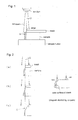
- Fig. 1 Japanese Patent No. 3263920
- the apparatus uses a mask in the form of a flat plate. This mask is made of a shielding material, has a straight edge, and is placed over a sample. The sample is etched by an ion beam directed at it with the boundary defined by the edge of the mask. The hatched portion in the figure is a portion of the sample to be etched to obtain a sample cross section S.
- Fig. 2 shows the process in which the sample is etched by the apparatus shown in Fig. 1.
- the sample is etched from its one corner.
- the mask irradiated with the ion beam is etched from its one corner in the same way as the sample.
- the present invention has been made. It would be desirable to provide a mask and a sample preparation apparatus capable of preparing a sample having a desired cross section by the use of the mask and by ion milling.
- a mask as specified in claim 1 This mask for the sample preparation apparatus that addresses the above-described aim is placed on the sample surface irradiated with an ion beam and has an edge portion that defines the boundary between a region irradiated with ions and an unirradiated region on the surface of the sample.
- the edge portion is made thicker than the other portions.
- the present invention provides the mask that is for use with the sample preparation apparatus and permits preparation of a sample having a desired cross section.
- the sample preparation apparatus is also offered, in accordance with a second aspect of the present invention.
- a method of preparing a sample as specified in claim 5 is provided.
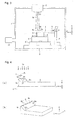
- Fig. 3 shows a sample preparation apparatus utilizing ion milling and built in accordance with one embodiment of the present invention.
- the apparatus has a vacuum chamber 1.
- An ion gun 2 is mounted on the top of the chamber 1.
- a gas ion gun is used as the ion gun 2.
- the gas ion gun ionizes Ar gas by electric discharge and releases Ar ions.
- the apparatus further includes a sample stage 3 on which an XY drive mechanism 4 capable of moving in the X- and Y-directions is disposed.
- a sample holder 5, which holds a sample 6, is set on the XY drive mechanism 4.
- a mask drive mechanism 7 is disposed on the sample stage 3 and can move in the Y-direction.
- a mask-holding portion 9 holding a mask 8 made of a shielding material is mounted to the mask drive mechanism 7 so as to be tiltable (that is rotatable) about an axis labelled a parallel to the X-axis.
- the mask-holding portion 9 has been tilted (that is rotated down) toward the sample 6.
- the mask 8 is placed over the sample 6 and in intimate contact with it.
- a pumping system 10 evacuates the inside of the vacuum chamber 1.
- Fig. 4 illustrates the mask 8 placed on the sample 6 shown in Fig. 3.
- (a) is a view as taken from a side (-X-direction) of the mask 8
- (b) is a perspective view of the mask 8.
- a surface 8a of the mask is irradiated with the ion beam I B from the ion gun 2 and has an edge portion 8b that is thicker than the other portions of the mask.
- the thickness of the edge portion 8b increases with approaching its one edge e.
- the edge portion 8b has a tilted, or sloping, surface 8b' parallel to the X-axis.
- the angle ⁇ made between the tilted surface 8b' and the Z-axis is about 30 degrees in the embodiment of Fig.4.
- the thickness h 1 of the portion forming the tilted surface 8b' is about 0.5 mm.
- the top surface 8b" of the edge portion 8b is parallel to the XY-plane.
- the lateral width (length taken in the Y-direction) d 1 of the top surface 8b" is about 50 ⁇ m.
- the edge portion 8b has a truncated triangle shape, or trapezium shape, in cross-section in the preferred embodiment.
- the mask is so machined that when it is brought into intimate contact with the sample surface, the side surface 8c of the mask forms a plane that is substantially perpendicular to the sample surface.
- the mask 8 can be fabricated, for example, by machining a magnetic material such as Super Inver (Co-Ni alloy) into a shape as shown in Fig. 4 and then firmly fixing an amorphous metal on the surface by nickel-phosphorus electroless plating (more than 10% phosphorus).
- the Super Inver is used for the following reasons. It has a quite small coefficient of thermal expansion. If the temperature rises due to ion beam irradiation, the resulting thermal deformation is small. The position of the edge varies little. Furthermore, it is easy to plate the material with a nickel-phosphorus alloy.
- the amorphous metal is used because during etching, the etching does not progress in a certain direction but progresses uniformly.
- the mask 8 can also be fabricated by machining a single-crystal material such as sapphire into a shape as shown in Fig. 4.
- a single-crystal material such as sapphire
- the sample 6 is machined by the ion beam with the sample preparation apparatus shown in Fig. 3 in the manner described below.
- the sample has a portion b to be etched to obtain a desired cross section S, the portion b being indicated by hatching.
- the mask and ion beam have been aligned relative to each other such that the side surface 8c of the mask lies on the center axis O of the ion beam I B .
- the inside of the vacuum chamber 1 is pumped down to a given degree of vacuum by the pumping system 10. Then, the ion beam I B is emitted from the ion gun 2 and hits both the sample 6 and mask 8.
- the portion of the beam I B not shielded by the mask 8 etches the surface of the sample 6. That is, the processed portion b of the sample 6 is etched by the beam I B hitting the sample 6 with the boundary defined by the edge e of the mask 8.
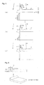
- Fig. 5 illustrates the process in which the processed portion b of the sample 6 is etched.
- the initial phase of the etching is shown at (a) of Fig. 5. During this initial phase, the processed portion b of the sample 6 is etched from its one corner.
- the portion of the mask irradiated with the ion beam I B is etched together with the sample.
- the edge portion 8b is tilted, or sloped, such that the thickness decreases with going away from the edge e and so ions hitting the top portion of the edge portion are reflected mainly away from the edge.
- the side surface of the mask is mainly etched.
- the original shape of the mask assumed prior to the irradiation of the ion beam is indicated by the broken line.
- the edge portion 8b of the mask 8 irradiated with the beam I B is etched while the original shape is substantially maintained.
- FIG. 5 shows a state occurring after a lapse of certain time since the state shown at (a).
- the edge portion 8b of the mask 8 has been etched further compared with the state shown at (a).
- the edge portion 8b of the mask 8 has been etched while the original shape assumed prior to the ion beam irradiation (indicated by the broken line) is substantially maintained.
- the thickness h 2 of the side surface 8c of the mask has been reduced slightly by the ion etching.
- the side surface 8c of the mask remains on the center axis O of the beam I B .
- the sample 6 is etched such that the desired cross section S appears.
- the sample 6 and mask 8 are etched as shown at (c) of Fig. 5.
- the edge portion 8b of the mask 8 has been etched while the original shape prior to the ion beam irradiation is substantially maintained.
- the side surface 8c of the mask remains on the center axis O of the beam I B .
- a sample having the desired cross section S is prepared.
- the cross section S of the sample will be observed later with a scanning electron microscope or other instrument.
- the method of processing the sample 6 by the ion beam with the sample preparation apparatus of Fig. 3 has been described so far. Since the preparation apparatus of Fig. 3 uses the inventive mask shown in Fig. 4, a sample having the desired cross section as described above and adapted for observation with an electron microscope can be prepared.
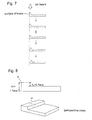
- the mask shown in Fig. 4 has the top surface 8b" .
- a mask having a sharp edge e not having the top surface 8b" may also be used.
- This mask shown in Fig. 6 is similar to the mask shown in Fig. 4 in other respects.
- the present invention embraces a mask having an edge portion of a shape as shown in Fig. 8.
- the edge portion of the mask shown in Fig. 8 has a rectangular cross section d .
- the cross-sectional shape is generally triangular, or wedge-shaped.
- the thickness of the whole mask may be made greater than conventional to address the aims of the invention. If such a mask is fabricated, the cost will be increased greatly. Accordingly, in the mask according to the preferred embodiment of the invention, only the edge portion is thickened.
- sample preparation apparatus may be used for preparation of samples observed with a transmission electron microscope, electron probe microanalyzer, Auger microprobe, or other similar instrument.
Landscapes
- Physics & Mathematics (AREA)
- Health & Medical Sciences (AREA)
- Life Sciences & Earth Sciences (AREA)
- Chemical & Material Sciences (AREA)
- Analytical Chemistry (AREA)
- Biochemistry (AREA)
- General Health & Medical Sciences (AREA)
- General Physics & Mathematics (AREA)
- Immunology (AREA)
- Pathology (AREA)
- Sampling And Sample Adjustment (AREA)
Applications Claiming Priority (2)
| Application Number | Priority Date | Filing Date | Title |
|---|---|---|---|
| JP2003296332A JP4037809B2 (ja) | 2003-08-20 | 2003-08-20 | イオンミーリング試料作製装置用マスクおよび試料作製装置 |
| JP2003296332 | 2003-08-20 |
Publications (3)
| Publication Number | Publication Date |
|---|---|
| EP1512957A2 true EP1512957A2 (de) | 2005-03-09 |
| EP1512957A3 EP1512957A3 (de) | 2005-11-16 |
| EP1512957B1 EP1512957B1 (de) | 2012-01-04 |
Family
ID=34131778
Family Applications (1)
| Application Number | Title | Priority Date | Filing Date |
|---|---|---|---|
| EP04255023A Expired - Lifetime EP1512957B1 (de) | 2003-08-20 | 2004-08-20 | Maske und diese verwendende Vorrichtung zur Vorbereitung von Proben durch Ionenbeschuss |
Country Status (3)
| Country | Link |
|---|---|
| US (1) | US7354500B2 (de) |
| EP (1) | EP1512957B1 (de) |
| JP (1) | JP4037809B2 (de) |
Cited By (1)
| Publication number | Priority date | Publication date | Assignee | Title |
|---|---|---|---|---|
| EP2264425A1 (de) * | 2009-06-18 | 2010-12-22 | Nobel Biocare Services AG | Verfahren und Anordnung zum Polieren einer Implantatprobe |
Families Citing this family (22)
| Publication number | Priority date | Publication date | Assignee | Title |
|---|---|---|---|---|
| JP4037809B2 (ja) * | 2003-08-20 | 2008-01-23 | 日本電子株式会社 | イオンミーリング試料作製装置用マスクおよび試料作製装置 |
| JP4557130B2 (ja) * | 2003-09-16 | 2010-10-06 | 日本電子株式会社 | 試料作製装置 |
| JP4553739B2 (ja) * | 2005-01-20 | 2010-09-29 | 日本電子株式会社 | 試料ホルダおよびイオンビーム加工装置 |
| JP2007248091A (ja) * | 2006-03-14 | 2007-09-27 | Jeol Ltd | 試料作製装置及び試料作成方法 |
| JP2007333682A (ja) * | 2006-06-19 | 2007-12-27 | Jeol Ltd | イオンビームを用いた断面試料作製装置 |
| JP4675860B2 (ja) * | 2006-08-09 | 2011-04-27 | 株式会社日立ハイテクノロジーズ | イオンミリング装置及びその方法 |
| US7803229B2 (en) * | 2007-02-15 | 2010-09-28 | Himax Display, Inc. | Apparatus and method for compensating uniformity of film thickness |
| JP4851365B2 (ja) * | 2007-03-02 | 2012-01-11 | 日本電子株式会社 | イオンミーリング試料作製装置用マスクおよび試料作製装置 |
| DE102008013511B4 (de) * | 2007-03-12 | 2018-11-22 | Hitachi High-Tech Science Corporation | Vorrichtung zum Bearbeiten und Beobachten von Proben sowie Verfahren zum Bearbeiten und Beobachten von Querschnitten |
| DE112010003115B4 (de) | 2009-07-30 | 2019-11-21 | Hitachi High-Technologies Corporation | Abschirmung für eine Ionenätzvorrichtung sowie Ionenätzvorrichtung |
| GB201002645D0 (en) * | 2010-02-17 | 2010-03-31 | Univ Lancaster | Method and apparatus for ion beam polishing |
| US8445874B2 (en) * | 2010-04-11 | 2013-05-21 | Gatan Inc. | Ion beam sample preparation apparatus and methods |
| US8283642B2 (en) | 2010-04-11 | 2012-10-09 | Gatan, Inc. | Ion beam sample preparation apparatus and methods |
| US8653489B2 (en) | 2010-04-11 | 2014-02-18 | Gatan, Inc. | Ion beam sample preparation apparatus and methods |
| US8384050B2 (en) | 2010-04-11 | 2013-02-26 | Gatan, Inc. | Ion beam sample preparation thermal management apparatus and methods |
| US8878147B2 (en) * | 2010-09-07 | 2014-11-04 | Joseph C. Robinson | Method and apparatus for in situ preparation of serial planar surfaces for microscopy |
| US10110854B2 (en) | 2012-07-27 | 2018-10-23 | Gatan, Inc. | Ion beam sample preparation apparatus and methods |
| US8791438B2 (en) | 2012-07-27 | 2014-07-29 | Gatan Inc. | Ion beam sample preparation apparatus and methods |
| CN105264632B (zh) * | 2013-06-10 | 2017-03-08 | 株式会社日立高新技术 | 离子碾磨装置 |
| DE102015219298B4 (de) * | 2015-10-06 | 2019-01-24 | Fraunhofer-Gesellschaft zur Förderung der angewandten Forschung e.V. | Verfahren zur Präparation einer Probe für die Mikrostrukturdiagnostik sowie Probe für die Mikrostrukturdiagnostik |
| JP7583002B2 (ja) | 2022-09-16 | 2024-11-13 | 日本電子株式会社 | 試料加工装置、遮蔽板、および試料加工方法 |
| TWI893753B (zh) * | 2024-04-10 | 2025-08-11 | 力晶積成電子製造股份有限公司 | 用於製備tem樣品的工具 |
Citations (2)
| Publication number | Priority date | Publication date | Assignee | Title |
|---|---|---|---|---|
| EP0626721A1 (de) | 1993-04-06 | 1994-11-30 | Siemens Aktiengesellschaft | Verfahren zur Erzeugung eines Oberflächenprofils in einer Oberfläche eines Substrats |
| US5907157A (en) | 1996-02-01 | 1999-05-25 | Jeol Ltd. | Method and apparatus for preparing specimen |
Family Cites Families (18)
| Publication number | Priority date | Publication date | Assignee | Title |
|---|---|---|---|---|
| AT371947B (de) * | 1979-12-27 | 1983-08-10 | Rudolf Sacher Ges M B H | Freitragende maske, verfahren zur herstellung derselben und verfahren zum maskieren von substraten |
| US4719498A (en) * | 1984-05-18 | 1988-01-12 | Fujitsu Limited | Optoelectronic integrated circuit |
| JPS6231854A (ja) * | 1985-08-02 | 1987-02-10 | Nec Corp | 液晶表示電極基板の製造方法 |
| ATA331085A (de) * | 1985-11-13 | 1994-05-15 | Ims Ionen Mikrofab Syst | Teilchen- oder strahlenbelastbare maske und verfahren zur herstellung derselben |
| JPS62279633A (ja) * | 1986-05-28 | 1987-12-04 | Fujitsu Ltd | パタ−ン形成方法 |
| DE3639346A1 (de) * | 1986-11-18 | 1988-05-26 | Siemens Ag | Verfahren und anordnung zur aenderung des abbildungsmassstabes in der roentgenlithografie |
| JPH11511868A (ja) * | 1995-05-30 | 1999-10-12 | アイエムエス イオネン ミクロファブリカティオーンス システメ ゲゼルシャフト エム・ベー・ハー | パターン構造を有するマスクの製造方法 |
| US5940678A (en) * | 1997-01-14 | 1999-08-17 | United Microelectronics Corp. | Method of forming precisely cross-sectioned electron-transparent samples |
| US5831272A (en) * | 1997-10-21 | 1998-11-03 | Utsumi; Takao | Low energy electron beam lithography |
| JP3454170B2 (ja) * | 1998-10-23 | 2003-10-06 | 松下電器産業株式会社 | 圧電素子の電極形成方法 |
| US6768110B2 (en) * | 2000-06-21 | 2004-07-27 | Gatan, Inc. | Ion beam milling system and method for electron microscopy specimen preparation |
| US6786978B2 (en) * | 2000-08-03 | 2004-09-07 | Texas Instruments Incorporated | Mass production of cross-section TEM samples by focused ion beam deposition and anisotropic etching |
| US7158701B2 (en) * | 2001-02-21 | 2007-01-02 | Shipley Company, L.L.C. | Method for making optical devices with a moving mask and optical devices made thereby |
| US6716656B2 (en) * | 2001-09-04 | 2004-04-06 | The Trustees Of Princeton University | Self-aligned hybrid deposition |
| JP4037809B2 (ja) * | 2003-08-20 | 2008-01-23 | 日本電子株式会社 | イオンミーリング試料作製装置用マスクおよび試料作製装置 |
| JP4557130B2 (ja) * | 2003-09-16 | 2010-10-06 | 日本電子株式会社 | 試料作製装置 |
| JP4486462B2 (ja) * | 2004-09-29 | 2010-06-23 | 日本電子株式会社 | 試料作製方法および試料作製装置 |
| JP4594156B2 (ja) * | 2005-04-21 | 2010-12-08 | 日本電子株式会社 | 試料作製方法および試料作製装置 |
-
2003
- 2003-08-20 JP JP2003296332A patent/JP4037809B2/ja not_active Expired - Lifetime
-
2004
- 2004-08-20 US US10/922,363 patent/US7354500B2/en not_active Expired - Lifetime
- 2004-08-20 EP EP04255023A patent/EP1512957B1/de not_active Expired - Lifetime
Patent Citations (3)
| Publication number | Priority date | Publication date | Assignee | Title |
|---|---|---|---|---|
| EP0626721A1 (de) | 1993-04-06 | 1994-11-30 | Siemens Aktiengesellschaft | Verfahren zur Erzeugung eines Oberflächenprofils in einer Oberfläche eines Substrats |
| US5907157A (en) | 1996-02-01 | 1999-05-25 | Jeol Ltd. | Method and apparatus for preparing specimen |
| JP3263920B2 (ja) | 1996-02-01 | 2002-03-11 | 日本電子株式会社 | 電子顕微鏡用試料作成装置および方法 |
Cited By (1)
| Publication number | Priority date | Publication date | Assignee | Title |
|---|---|---|---|---|
| EP2264425A1 (de) * | 2009-06-18 | 2010-12-22 | Nobel Biocare Services AG | Verfahren und Anordnung zum Polieren einer Implantatprobe |
Also Published As
| Publication number | Publication date |
|---|---|
| JP2005062131A (ja) | 2005-03-10 |
| US20050081997A1 (en) | 2005-04-21 |
| US7354500B2 (en) | 2008-04-08 |
| EP1512957B1 (de) | 2012-01-04 |
| EP1512957A3 (de) | 2005-11-16 |
| JP4037809B2 (ja) | 2008-01-23 |
Similar Documents
| Publication | Publication Date | Title |
|---|---|---|
| EP1512957A2 (de) | Maske und diese verwendende Vorrichtung zur Vorbereitung von Proben durch Ionenbeschuss | |
| Stevie et al. | Application of focused ion beam lift‐out specimen preparation to TEM, SEM, STEM, AES and SIMS analysis | |
| US7722818B2 (en) | Apparatus and method for preparing samples | |
| KR100253145B1 (ko) | 표본 분리방법과, 표본 분리방법으로 분리된 표본의 분석방법 | |
| KR101463245B1 (ko) | 집중 이온빔 장치 및 그것을 이용한 시료 단면 제작 방법및 박편 시료 제작 방법 | |
| JP6629596B2 (ja) | エッチング速度を変化させるためのイオン注入 | |
| EP1804273B1 (de) | Verfahren zur Probenherstellung | |
| US6417512B1 (en) | Sample distortion removing method in thin piece forming | |
| KR100796829B1 (ko) | 투과형 전자 현미경 시료 박편화 가공방법 | |
| WO2002071031B1 (en) | Total release method for sample extraction from a charged particle instrument | |
| US7705329B2 (en) | Charged particle beam processing apparatus | |
| JPH11108813A (ja) | 試料作製方法および装置 | |
| EP1684327B1 (de) | Probenhalter und Ionenstrahlverarbeitungssystem | |
| US6576894B1 (en) | Structure for FIB based microanalysis and method for manufacturing it | |
| JP3103319B2 (ja) | サイクロトロン用ストリッピングフォイルの製造方法 | |
| US5747803A (en) | Method for preventing charging effect and thermal damage in charged-particle microscopy | |
| CN110581088B (zh) | 用于表面平坦化的方法和设备 | |
| US6683305B1 (en) | Method to obtain transparent image of resist contact hole or feature by SEM without deforming the feature by ion beam | |
| JP2004179038A (ja) | 透過電子顕微鏡用試料の固定方法および試料台 | |
| JPH11329325A (ja) | メッシュおよび薄片試料の作製方法 | |
| JPH08261894A (ja) | Tem評価試料及びその作成方法 | |
| JPH0462748A (ja) | 電子顕微鏡用試料加工方法、及び集束イオンビーム加工装置 | |
| JP2001141620A (ja) | 透過電子顕微鏡用試料の切り込み加工法 | |
| EP4339993A1 (de) | Ionenfräsvorrichtung, abschirmungsplatte und verfahren zur herstellung einer probe durch eine ionenfräsvorrichtung | |
| EP1612836B1 (de) | Methode zum Entfernen einer mikroskopischen Probe von einem Substrat |
Legal Events
| Date | Code | Title | Description |
|---|---|---|---|
| PUAI | Public reference made under article 153(3) epc to a published international application that has entered the european phase |
Free format text: ORIGINAL CODE: 0009012 |
|
| AK | Designated contracting states |
Kind code of ref document: A2 Designated state(s): AT BE BG CH CY CZ DE DK EE ES FI FR GB GR HU IE IT LI LU MC NL PL PT RO SE SI SK TR |
|
| AX | Request for extension of the european patent |
Extension state: AL HR LT LV MK |
|
| PUAL | Search report despatched |
Free format text: ORIGINAL CODE: 0009013 |
|
| AK | Designated contracting states |
Kind code of ref document: A3 Designated state(s): AT BE BG CH CY CZ DE DK EE ES FI FR GB GR HU IE IT LI LU MC NL PL PT RO SE SI SK TR |
|
| AX | Request for extension of the european patent |
Extension state: AL HR LT LV MK |
|
| RIC1 | Information provided on ipc code assigned before grant |
Ipc: 7H 01J 37/305 B Ipc: 7G 01N 1/32 A |
|
| 17P | Request for examination filed |
Effective date: 20060405 |
|
| AKX | Designation fees paid |
Designated state(s): DE FR |
|
| 17Q | First examination report despatched |
Effective date: 20061018 |
|
| GRAP | Despatch of communication of intention to grant a patent |
Free format text: ORIGINAL CODE: EPIDOSNIGR1 |
|
| GRAS | Grant fee paid |
Free format text: ORIGINAL CODE: EPIDOSNIGR3 |
|
| GRAA | (expected) grant |
Free format text: ORIGINAL CODE: 0009210 |
|
| RAP1 | Party data changed (applicant data changed or rights of an application transferred) |
Owner name: JEOL LTD. |
|
| AK | Designated contracting states |
Kind code of ref document: B1 Designated state(s): DE FR |
|
| REG | Reference to a national code |
Ref country code: DE Ref legal event code: R096 Ref document number: 602004035956 Country of ref document: DE Effective date: 20120308 |
|
| PLBE | No opposition filed within time limit |
Free format text: ORIGINAL CODE: 0009261 |
|
| STAA | Information on the status of an ep patent application or granted ep patent |
Free format text: STATUS: NO OPPOSITION FILED WITHIN TIME LIMIT |
|
| 26N | No opposition filed |
Effective date: 20121005 |
|
| REG | Reference to a national code |
Ref country code: DE Ref legal event code: R097 Ref document number: 602004035956 Country of ref document: DE Effective date: 20121005 |
|
| REG | Reference to a national code |
Ref country code: FR Ref legal event code: PLFP Year of fee payment: 13 |
|
| REG | Reference to a national code |
Ref country code: FR Ref legal event code: PLFP Year of fee payment: 14 |
|
| REG | Reference to a national code |
Ref country code: FR Ref legal event code: PLFP Year of fee payment: 15 |
|
| PGFP | Annual fee paid to national office [announced via postgrant information from national office to epo] |
Ref country code: FR Payment date: 20230822 Year of fee payment: 20 Ref country code: DE Payment date: 20230821 Year of fee payment: 20 |
|
| REG | Reference to a national code |
Ref country code: DE Ref legal event code: R071 Ref document number: 602004035956 Country of ref document: DE |