EP1515325A2 - Verfahren zum Herstellen eines optischen Vielschicht-Aufzeichnungsmediums und eines Zwischenprodukts im Herstellungsverfahren desselben - Google Patents
Verfahren zum Herstellen eines optischen Vielschicht-Aufzeichnungsmediums und eines Zwischenprodukts im Herstellungsverfahren desselben Download PDFInfo
- Publication number
- EP1515325A2 EP1515325A2 EP04021369A EP04021369A EP1515325A2 EP 1515325 A2 EP1515325 A2 EP 1515325A2 EP 04021369 A EP04021369 A EP 04021369A EP 04021369 A EP04021369 A EP 04021369A EP 1515325 A2 EP1515325 A2 EP 1515325A2
- Authority
- EP
- European Patent Office
- Prior art keywords
- manufacturing
- circular projection
- spacer layer
- substrate
- optical recording
- Prior art date
- Legal status (The legal status is an assumption and is not a legal conclusion. Google has not performed a legal analysis and makes no representation as to the accuracy of the status listed.)
- Withdrawn
Links
Images


Classifications
-
- G—PHYSICS
- G11—INFORMATION STORAGE
- G11B—INFORMATION STORAGE BASED ON RELATIVE MOVEMENT BETWEEN RECORD CARRIER AND TRANSDUCER
- G11B7/00—Recording or reproducing by optical means, e.g. recording using a thermal beam of optical radiation by modifying optical properties or the physical structure, reproducing using an optical beam at lower power by sensing optical properties; Record carriers therefor
- G11B7/24—Record carriers characterised by shape, structure or physical properties, or by the selection of the material
- G11B7/26—Apparatus or processes specially adapted for the manufacture of record carriers
-
- G—PHYSICS
- G11—INFORMATION STORAGE
- G11B—INFORMATION STORAGE BASED ON RELATIVE MOVEMENT BETWEEN RECORD CARRIER AND TRANSDUCER
- G11B7/00—Recording or reproducing by optical means, e.g. recording using a thermal beam of optical radiation by modifying optical properties or the physical structure, reproducing using an optical beam at lower power by sensing optical properties; Record carriers therefor
- G11B7/24—Record carriers characterised by shape, structure or physical properties, or by the selection of the material
- G11B7/2403—Layers; Shape, structure or physical properties thereof
- G11B7/24035—Recording layers
- G11B7/24038—Multiple laminated recording layers
Definitions
- the present invention relates to a method for manufacturing a multilayer recording type optical recording medium having a central hole, in which a spacer layer and a light transmitting layer are formed on a substrate in that order, and an intermediate in a manufacturing process of the optical recording medium.
- optical recording media such as CDs (Compact Disc), DVDs (Digital Versatile Disc), and the like, have spread rapidly.
- Typical optical media have an outer diameter of 120 mm and a thickness of 1.2 mm that are standardized.
- laser light having a shorter wavelength than that for a CD is used as illumination light and numerical aperture of a lens for the illumination light is made larger than that for a CD.
- s DVD enables the larger amount of information to be recorded and reproduced with higher density, as compared with CDs.
- a DVD employs a light transmitting layer having a thickness of 0.6 mm, which is a half of that in a CD, so as to ensure margin for the tilt (warp) of the disc, thereby maintaining the precision of the recording and reproducing information.
- the light transmitting layer having a thickness of 0.6 mm cannot provide sufficient stiffness and strength by itself to DVD.
- a DVD is formed by bonding two substrates having a thickness of 0.6 mm to each other with their information recording surfaces arranged inside so as to have a total thickness of 1.2 mm that is the same as CD. In this manner, in a DVD, the stiffness and strength that are substantially equal to those of a CD are ensured.
- a spacer layer can be formed between substrates, and information can be recorded on both sides of the spacer layer while the substrates are bonded to each other. By employing such a double-sided recording type structure, it is possible to record the larger amount of information with higher density on a DVD.
- the central hole is formed simultaneously with a molding process in which a substrate is molded to be a circular disk, and is used not only for positioning the optical recording medium in a recording and reproducing apparatus but also for transfer, storage and the like, of the optical recording medium in a manufacturing process.
- an optical recording medium In order to achieve recording of the larger amount of information with higher recording density, an optical recording medium has now drawn attention, for which the wavelength of the illumination light is made further shorter and the numerical aperture of the lens is further increased.
- a further thinner light transmitting layer is formed in accordance with the shorter wavelength of the illumination light and the increased numerical aperture (see Japanese Patent Laid-Open Publication No. 2003-85836, for example).
- an optical recording medium has spread, for which blue-violet laser light having a wavelength of 405 nm is used as illumination light and the numerical aperture is set to 0.85, and which includes a light transmitting layer having a thickness of 0.1 mm in accordance with these conditions.
- a multilayer recording type structure can be achieved by forming the spacer layer on one surface or both surfaces of the substrate and forming recording layers on both sides of the spacer layer, as in DVD.
- the thickness of the substrate, that of the spacer layer, that of the light transmitting layer be set to approximately 1.1 mm, approximately 25 ⁇ m, and approximately 75 ⁇ m, respectively.
- variation in the thickness of the multilayer structure, i.e., the spacer layer and the light transmitting layer be within ⁇ 2 ⁇ m. That is, it is demanded that the difference between the minimum thickness and the maximum thickness of the multilayer structure be 4 ⁇ m or less.
- a method for forming such a thin light transmitting layer that is as thin as 75 ⁇ m, the following methods are considered.
- One method is to bond a film of polycarbonate or the like to a substrate.
- Another method is to spread a resin that can be cured by radiation such as UV (ultraviolet) rays or electron beams, on a substrate by spin-coating and then cure that resin by irradiating radiation.
- the latter method is preferable for forming a light transmitting layer because that method is good in production efficiency, can be performed at a lower cost, can provide a good tracking performance, and the like.
- the spin-coating method is adopted to a substrate having a central hole formed therein, the thickness of the light transmitting layer is liable to become uneven. Thus, the recording and reproducing of the information with high density may be difficult to perform.
- the excess amount of resin is supplied from an inner region.
- the thickness of the resultant layer does not become uniform. That is, the resultant layer is thinner in the inner region than in the outer region.
- the resin is additionally supplied to the inner region.
- control has to be done with high precision in accordance with variation in the thickness of the resultant layer. It is practically impossible to perform such control.
- a part of the resin may enter the central hole so as to generate radial streaks and the like, in the light transmitting layer, for example, thus degrading the appearance of the light transmitting layer.
- the substrate is molded in the form of a disk having no central hole and thereafter a resin is supplied to the center of the substrate or to a portion inner than the portion where the resin is supplied in the case in which the substrate has the central hole, the resin can be spread with a uniform thickness.
- the central hole can be formed by punching out a hole in the light transmitting layer and the substrate with a tool.
- the substrate having no central hole has a problem that such a substrate is difficult to transfer, store and the like, in a manufacturing process of the optical recording medium and decreases production efficiency. Moreover, it is difficult to position the substrate having no central hole with high precision. In addition, the amount of eccentricity of the central hole tends to become larger when the central hole is formed in a later process.
- various exemplary embodiments of this invention provide a method for manufacturing a multilayer recording type optical recording medium and an intermediate in a manufacturing process of the optical recording medium, which can form a spacer layer and a light transmitting layer with a uniform thickness and can provide good production efficiency.
- a circular projection having an outer diameter smaller than an inner diameter of a central hole is formed integrally with a spacer layer in the vicinity of a center of the spacer layer. Then, a radiation curable resin is supplied to a region around the circular projection and at the same time a substrate is rotated, thereby a light transmitting layer is spread over the spacer layer. In this manner, the aforementioned object can be achieved.
- radioactive element such as ⁇ -ray, X-ray, ⁇ -ray or the like.
- radiation herein is used as a general term of an electromagnetic wave and a particle beam that have a nature for curing a specific resin that is fluid, such as UV rays, and electron beams.
- the circular projection is formed together with the spacer layer in a process for forming the spacer layer.
- the circular projection does not obstruct the formation of the spacer layer having a uniform thickness. Therefore, the spacer layer having the uniform thickness can be formed.
- the radiation curable resin that is a material for the light transmitting layer is supplied to the region near the circular projection having the outer diameter smaller than the central hole. Thus, centrifugal force acting on the resin in the region where the resin is supplied is small.
- the resin is hard to move away from the circular projection because of its viscosity, it is possible to prevent the resin in a region near the center of the substrate from becoming drastically thinner. Therefore, the light transmitting layer can be spread with a uniform thickness.
- the present exemplary embodiment has a feature in a method for manufacturing an optical recording medium 10 as shown in Fig. 1, and in a structure of an intermediate in a manufacturing process of the optical recording medium 10.
- the structure of the optical recording medium 10 will be briefly described.
- the optical recording medium 10 is a disk having an outer diameter of approximately 120 mm and a thickness of approximately 1.2 mm, and has a central hole 10A having an inner diameter of approximately 15 mm.
- the optical recording medium 10 is a single-sided two-layer recording type in which a spacer layer 14 and a light transmitting layer 16 are formed on one surface of a substrate 12 in that order.
- the substrate 12 is formed of a resin such as polycarbonate, acrylic resin, epoxy resin, and has a thickness of approximately 1.1 mm.
- fine concave and convex portions (not shown) for carrying information, such as pits and grooves.
- pits and grooves are generally used to mean concave portions for carrying information, those terms are used herein to mean not only the concave portions but also convex portions for carrying information for convenience.
- a first functional layer is formed on the first information recording surface 12A of the substrate 12.
- the first functional layer is thinner than the spacer layer 14 and the light transmitting layer 16 and appears to be needless to understand the present invention, the first functional layer is not shown in the drawings.
- the optical recording medium 10 is a ROM (Read Only Memory) type disc
- a reflection layer of Al, Ag, Au or the like is formed as the functional layer on the information recording surface 12A.
- RW Re-Writable
- a recording layer made of a phase change material, a magneto-optical material or the like is formed in addition to the reflection layer.
- an R (Recordable) type disc a recording layer made of phase change material or including organic dye is formed in addition to the reflection layer.
- the spacer layer 14 is formed on the first information recording surface 12A with the first functional layer interposed therebetween and has a thickness of approximately 25 ⁇ m.
- the spacer layer 14 is formed of a material that can be cured by radiation and can transmit light, such as an acrylic UV (ultraviolet) curable resin and an epoxy UV curable resin.
- An opposite surface of the spacer layer 14 to the substrate 12 serves as a second information recording surface 14A where fine concave and convex portions for carrying information, such as pits and grooves, are formed.
- a second functional layer (not shown) is formed like the first functional layer on the first information recording surface 12A.
- the light transmitting layer 16 is formed on the second information recording surface 14A with the second functional layer interposed therebetween and has a thickness of approximately 75 ⁇ m.
- the light transmitting layer 16 is also formed of a material that can be cured by radiation and can transmit light, such as an acrylic UV curable resin, like the spacer layer 14.
- a substrate 12 in the form of a circular disc having an outer diameter of approximately 120 mm and a thickness of approximately 1.1 mm, shown in Fig. 3, is molded by injection molding (Step S102).
- fine concave and convex portions for carrying information are transferred onto the first surface of the substrate 12, thereby forming the information recording surface 12A.
- a circular concave portion 12C having the same inner diameter as that of the central hole 10A is also formed on an opposite surface to the first information recording surface 12A.
- a manufacturing hole 12B having an inner diameter smaller than the central hole 10A is simultaneously formed.
- the manufacturing hole 12B may be formed in the injection-molded substrate 12 by means of a tool or the like.
- the thus obtained a plurality of substrates 12 are usually stored or transferred while being stacked.
- a guide in the form of a round bar or the like, into the manufacturing hole 12B it is easy to stack a plurality of substrates 12 while they are aligned. This makes the storage or transfer of the substrates easier, thus improving production efficiency.
- a functional layer (not shown) is formed by sputtering, deposition, or the like (Step S104).
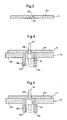
- the substrate 12 is horizontally placed on a rotating table 18 with the information recording surface 12A faced upward.
- the rotating table 18 has a structure in which a shaft 18B projects downward from a table part 18A in the form of a circular disk placed horizontally. Within the shaft 18B, a vent hole 18C is formed to be in communication with the table part 18A. The shaft 18B is engaged with a rotating driving mechanism that is not shown. Moreover, to the vent hole 18C, a negative-pressure supply that is not shown is connected.
- the core member 20 is a round bar having an outer diameter slightly smaller than the inner diameter of the manufacturing hole 12B in its original state, and can be fitted into the manufacturing hole 12B freely.
- the core member 20 is formed of a silicone resin, a fluororesin, an acrylic resin, an olefin resin or a mixture thereof, and has elasticity.
- the core member 20 has a hollow structure (not shown) in which the inside thereof is in communication with air supply means 24 at its lower end. When an air is supplied to the inside of the core member 20, the core member 20 expands and increases its outer diameter, so that the core member 20 comes into close contact with the inner circumference of the manufacturing hole 12B.
- the core member 20 is made to expand by the air supply means 24, so that the core member 20 is brought into close contact with the inner circumference of the manufacturing hole 12B. Then, a negative pressure is supplied to an upper surface of a table part 18A of the rotating table 18 so as to absorb the substrate 12 and fix it onto the rotating table 18.
- a predetermined amount of radiation curable resin that is fluid is supplied to a region near the center of the substrate 12. Moreover, a transparent stamper 26 is brought close to the first information recording surface of the substrate 12. Please note that the radiation curable resin does not enter a gap between the core member 20 and the substrate 12 because the core member 20 is in close contact with the manufacturing hole 12B.
- the transparent stamper 26 is an approximately circular plate formed of a material that can transmit light, such as an acrylic resin, an olefin resin, or glass.
- One surface of the transparent stamper 26 serves as a transfer surface 26A having a fine convex and concave pattern that is reverse to the pattern in the second information recording surface 14A.
- the transparent stamper 26 has a cylindrical projection 26B near its center, which projects toward the opposite direction to the transfer surface 26A. That projection 26B has an inner diameter that is larger than the manufacturing hole 12B and is smaller than the central hole 10A, and the information recording surface 26A side of the projection 26B is opened with that inner diameter.
- the opposite side of the projection 26B to the information recording surface 26A is also opened, it is partially closed.
- a through hole 26C is formed.
- the through hole 26C has an inner diameter that allows the through hole 26C to fit with the core member 20 freely.
- a space between the transparent stamper 26 and the substrate 12 is filled with a radiation curable resin, thereby forming a spacer layer 14.
- fine concave and convex portions are transferred onto an opposite surface of the spacer layer 14 to the substrate 12, so that the second information recording surface 14A is formed.
- fine concave and convex portions are also transferred to copy the pattern in the first information recording surface 12A.
- a circular projection 28 is formed integrally with the spacer layer 14 (Step S106).
- the circular projection 28 has an annular shape with an outer diameter smaller than the inner diameter of the central hole 10A.
- the outer diameter of the circular projection 28 be set to 10 mm or less.
- the outer diameter of the circular projection 28 is set to 8 mm or less, a margin is obtained.
- the uniformity of the thickness of the light transmitting layer can be further improved.
- the outer diameter of the circular projection 28 be set to 3 mm or more.
- the height of the circular projection 28 be set to 1 mm or more.
- the uniformity of the thickness of the light transmitting layer can be further improved.
- the effect that the light transmitting layer can be spread with a uniform thickness tends to be enhanced as the circular projection 28 becomes higher.
- the upper limit of the height of the circular projection 28 is preferably set to about 5 mm.
- the rotating table 18 may be rotated after the transparent stamper 26 was brought close to the first information recording surface of the substrate 12, so that the radiation curable resin is caused to flow outward in a radial direction by centrifugal force.
- the transparent stamper 26 approaches to the first information recording surface 12A of the substrate 12 because of a negative pressure.
- the rotation of the rotating table 18 can be stopped when the transparent stamper 26 reached a position away from the first information recording surface 12A by approximately 25 ⁇ m.
- the space between the transparent stamper 26 and the substrate 12 may be filled with the resin.
- Step S108 the rotation of the rotating table 18 is stopped, and the spacer layer 14 is uniformly irradiated with UV rays through the transparent stamper 26, so that the spacer layer 14 is cured.
- the core member 20 is formed of a silicone resin, a fluororesin, or the like, it is hard to adhere to the spacer layer 14. Thus, the substrate 12 and the core member 20 can be separated from each other easily.
- the intermediate 30 is dismounted from the rotating table 18. Then, the second functional layer (not shown) is formed on the second information recording surface 14A of the intermediate 30. This is achieved by sputtering, deposition or the like, as with the layer on the first information surface 12A (Step S110).
- the intermediate 30 is placed again on the rotating table 18.
- a nozzle 32 is brought close to a region near the circular projection 28.
- a predetermined amount of a radiation curable resin being fluid is supplied onto the second information recording surface 14A.
- the thus supplied radiation curable resin is then spread outward in the radial direction by centrifugal force.
- the amount of the flowing resin on the second information recording surface 14A is relieved and stabilized because the centrifugal force acting on the resin is smaller near the circular projection 28 (which has the outer diameter smaller than the central hole 10A) than near the outer circumference of the substrate 12.
- the resin adhering to the circular projection 28 tries to stay in the vicinity of the circular projection 28 because of its viscosity. This also enhances the effect that the amount of the flowing resin on the second information recording surface 14A is relieved.
- a light transmitting layer 16 is spread over the second information recording surface 14A with a uniform thickness of approximately 75 ⁇ m, as shown in Fig. 11 (Step S112).
- Step S114 the rotation of the rotating table 18 is stopped, and the light transmitting layer 16 thus spread is uniformly irradiated with radiation such as UV rays, so that the light transmitting layer 16 is cured.
- the substrate 12 is dismounted from the rotating table 18, a jig is fitted into the manufacturing hole 12B to position the substrate 12 (not shown). Then, as shown in Fig. 13, a circular tool 34 is placed on the substrate 12 concentrically with respect to the substrate 12.
- the circular tool 34 has an outer diameter equal to the size of the inner diameter of the central hole 10A
- the circular tool 34 is penetrated into the substrate 12 in an axial direction thereof, thereby punching out a hole that serves as the central hole 10A in the substrate 12 (Step S116). Since the circular concave portion 12C having the inner diameter equal to that of the central hole 10A is formed in the substrate 12 in advance, the penetration can be easily done. Moreover, by using the manufacturing hole 12B, the amount of eccentricity of the central hole 10A can be suppressed to be small.
- the core member 20 is formed of a silicon resin, a fluororesin, or the like and a round bar that has elasticity and has an outer diameter slightly smaller than the inner diameter of the manufacturing hole 12B in its original state, and can be freely fitted into the manufacturing hole 12B.
- the core member can come into close contact with the inner circumference of the manufacturing hole 12B, there is no restriction to the material and shape of the core member.
- an acrylic UV curable resin and an epoxy UV curable resin are described as exemplary materials for the spacer layer 14 and the light transmitting layer 16.
- other resins that can transmit light and can be cured by radiation such as electron-beam curable resin, may be used.
- the substrate is formed by injection molding, which includes the circular concave portion 12C having the same inner diameter as that of the central hole (that has the inner diameter larger than that of the manufacturing hole 12B), in the opposite surface to the information recording surface 12A.
- the substrate 12 in which the opposite surface to the information recording surface 12A is flat may be formed by injection molding.
- the manufacturing hole 12B is formed in the substrate 12 and the circular projection 28 is formed to be annular.
- the circular projection 28 may be formed to be cylindrical or in the form of a circular plate.
- the region in the vicinity of the circular projection 28 serves as a portion where the resin is reserved.
- the optical recording medium 10 in the present exemplary embodiment is a two-layer recording type which has a single spacer layer and recording layers provided on both sides of the spacer layer.
- the circular projection having the outer diameter smaller than the inner diameter of the central hole may be formed integrally with the uppermost spacer layer that is the closest one of a plurality of spacer layers to the light transmitting layer.
- the optical recording medium 10 is a single-sided two-layer recording type in which information can be recorded onto one surface of the optical recording medium 10.
- the present invention can be applied to a double-sided multilayer recording type optical recording medium in which information can be recorded on both surfaces of the medium.
- an optical recording medium having a total thickness of 1.2 mm can be obtained when a spacer layer having a thickness of 25 ⁇ m and a light transmitting layer having a thickness of 75 ⁇ m are formed on both surfaces of a substrate having a thickness of about 1.0 mm.
- Ten intermediates 30 were manufactured for each of respective ten outer diameters of the circular projection 28, i.e., 2.2 mm, 4 mm, 5 mm, 6 mm, 7 mm, 8 mm, 9 mm, 10 mm, 12 mm, and 14 mm, in the manner described in the above embodiment. Then, a light transmitting layer 16 was spread on the second information recording surface 14A of each intermediate 30 under a spin-coating condition in which revolutions per minute of the turntable 18 is approximately 2000 rpm. In this manner, 100 optical recording media 10 were fabricated.
- TMPTA trimethylolpropane triacrylate
- R-604 manufactured by Nippon Kayaku Co., Ltd.
- THF-A tetrahydrofurfuryl acrylate
- Irgacure® 184 manufactured by Ciba Specialty Chemicals K. K.
- Irgacure® 184 manufactured by Ciba Specialty Chemicals K. K.
- ART RESIN® UN-5200 manufactured by Negami Chemical Industrial Co., Ltd.
- 77 wt% ARONIX® M-315 manufactured by Toagosei Co., Ltd.
- 10 wt% THF-A manufactured by Kyoeisha Chemical Co., Ltd.
- Viscosity of the resin before curing 6800 mPa ⁇ s
- An average of the thickness of two layers, i.e., the spacer layer 14 and the light transmitting layer 16 in each optical recording medium 10 and a difference between the minimum thickness and the maximum thickness of those two layers in each optical recording medium 10 are shown in Table 1 for each outer diameter of the circular projection 28.
- the average and the difference shown in Table 1 are obtained as averaged values of thicknesses and thickness differences of ten optical recording media 10 having the circular projections 28 of the same outer diameter, respectively.
- the optical recording media 10 in which the light transmitting layers 16 looked good are shown with " ⁇ " in Table 1.
- the mark " ⁇ " represents that the appearance of the light transmitting layer 16 was good for all the ten optical recording media 10 having the circular projections 28 of the same outer diameter.
- the thickness difference was suppressed to 3 ⁇ m or less and the quality was better.
- all the 100 optical recording media 10 of this example had the light transmitting layers 16 that looked good, irrespective of the outer diameter of the circular projection 28.
- the optical recording media 10 having the light transmitting layers 16 that looked good are shown with " ⁇ ” while the optical recording media 10 having the light transmitting layers 16 that did not look good are shown with " ⁇ .”
- the mark “ ⁇ ” represents that the appearance of the light transmitting layer 16 was good for all the ten optical recording media 10 having the manufacturing holes 12B of the same inner diameter, while the mark “ ⁇ ” represents that the appearance of the light transmitting layer 16 was not good for a part of or all of the ten optical recording media 10 having the manufacturing holes 12B of the same inner diameter.
- the thickness difference of the light transmitting layer 16 exceeded 4 ⁇ m. That is, with respect to this point, the required quality was not obtained. Although the appearance of the light transmitting layer 16 was not good in the case where the inner diameter of the manufacturing hole 12B was 9 mm, it was good in the case where the inner diameter of the manufacturing hole 12B was 10 mm or more.
- the exemplary embodiments of the present invention can be used for forming a light transmitting layer with a uniform thickness in a multilayer recording type optical recoding medium.
Landscapes
- Engineering & Computer Science (AREA)
- Manufacturing & Machinery (AREA)
- Manufacturing Optical Record Carriers (AREA)
- Optical Record Carriers And Manufacture Thereof (AREA)
- Thermal Transfer Or Thermal Recording In General (AREA)
Applications Claiming Priority (2)
| Application Number | Priority Date | Filing Date | Title |
|---|---|---|---|
| JP2003318725 | 2003-09-10 | ||
| JP2003318725A JP2005085411A (ja) | 2003-09-10 | 2003-09-10 | 多層記録タイプの光記録媒体の製造方法及び製造工程における中間体 |
Publications (2)
| Publication Number | Publication Date |
|---|---|
| EP1515325A2 true EP1515325A2 (de) | 2005-03-16 |
| EP1515325A3 EP1515325A3 (de) | 2006-04-19 |
Family
ID=34132006
Family Applications (1)
| Application Number | Title | Priority Date | Filing Date |
|---|---|---|---|
| EP04021369A Withdrawn EP1515325A3 (de) | 2003-09-10 | 2004-09-08 | Verfahren zum Herstellen eines optischen Vielschicht-Aufzeichnungsmediums und eines Zwischenprodukts im Herstellungsverfahren desselben |
Country Status (3)
| Country | Link |
|---|---|
| US (1) | US20050053751A1 (de) |
| EP (1) | EP1515325A3 (de) |
| JP (1) | JP2005085411A (de) |
Families Citing this family (3)
| Publication number | Priority date | Publication date | Assignee | Title |
|---|---|---|---|---|
| JP3976655B2 (ja) * | 2002-09-27 | 2007-09-19 | Tdk株式会社 | 光記録媒体用中間体、成形金型、成形機、および光記録媒体の製造方法 |
| KR20060109453A (ko) * | 2003-11-03 | 2006-10-20 | 코닌클리케 필립스 일렉트로닉스 엔.브이. | 재기록가능한 광학 데이터 기억 매체 및 그 기억 매체의사용 |
| JP4859793B2 (ja) * | 2007-09-06 | 2012-01-25 | 株式会社リコー | 光記録媒体用の基板の製造方法 |
Family Cites Families (13)
| Publication number | Priority date | Publication date | Assignee | Title |
|---|---|---|---|---|
| US4877475A (en) * | 1984-11-01 | 1989-10-31 | Matsushita Electric Industrial Co., Ltd. | Method for producing information storage disk |
| JPH09134547A (ja) * | 1995-11-08 | 1997-05-20 | Sony Corp | 光学記録媒体およびその製造方法 |
| JPH09171634A (ja) * | 1995-12-20 | 1997-06-30 | Sony Disc Technol:Kk | 情報記録媒体及び情報記録媒体の製造方法 |
| DE69731707T2 (de) * | 1996-07-31 | 2006-03-02 | Kitano Engineering Co., Ltd., Komatsushima | Verfahren zum Korrigieren von der ungleichen Position einer Informationsscheibe |
| JP3918221B2 (ja) * | 1997-03-12 | 2007-05-23 | ソニー株式会社 | 保護膜形成装置及び保護膜形成方法 |
| KR100528112B1 (ko) * | 1997-08-20 | 2006-03-17 | 소니 가부시끼 가이샤 | 원반형 기록 매체의 제조 장치 및 방법 |
| JP2002063737A (ja) * | 2000-06-09 | 2002-02-28 | Tdk Corp | 光情報媒体およびその製造方法 |
| JP2003091887A (ja) * | 2001-09-20 | 2003-03-28 | Tdk Corp | 多層光記録媒体の製造方法および多層光記録媒体製造装置 |
| JP2003099991A (ja) * | 2001-09-27 | 2003-04-04 | Tdk Corp | 光記録媒体の製造方法および光記録媒体製造装置 |
| JP2003123331A (ja) * | 2001-10-04 | 2003-04-25 | Tdk Corp | 多層光記録媒体の製造方法および多層光記録媒体 |
| JP2003203401A (ja) * | 2001-12-28 | 2003-07-18 | Matsushita Electric Ind Co Ltd | 塗布方法、および樹脂層形成法 |
| KR100878519B1 (ko) * | 2002-01-19 | 2009-01-13 | 삼성전자주식회사 | 광디스크 제조 방법 |
| JP2003242694A (ja) * | 2002-02-15 | 2003-08-29 | Sony Corp | 光学記録媒体の製造方法 |
-
2003
- 2003-09-10 JP JP2003318725A patent/JP2005085411A/ja not_active Withdrawn
-
2004
- 2004-09-01 US US10/930,868 patent/US20050053751A1/en not_active Abandoned
- 2004-09-08 EP EP04021369A patent/EP1515325A3/de not_active Withdrawn
Also Published As
| Publication number | Publication date |
|---|---|
| US20050053751A1 (en) | 2005-03-10 |
| EP1515325A3 (de) | 2006-04-19 |
| JP2005085411A (ja) | 2005-03-31 |
Similar Documents
| Publication | Publication Date | Title |
|---|---|---|
| JP4338688B2 (ja) | 光情報記録媒体の製造方法 | |
| US6404730B2 (en) | Optical disk having a groove and a projection for combining two disk members | |
| US7161893B2 (en) | Stamper for fabrication of optical recording medium, method of forming information recording area and light transmissive layer, and optical recording medium | |
| JP2002170279A (ja) | 光学記録媒体およびその製造方法、ならびに射出成形装置 | |
| JP2002063737A (ja) | 光情報媒体およびその製造方法 | |
| US7221640B2 (en) | Method of manufacturing an optical storage medium and optical storage medium | |
| JP2006513516A (ja) | 光データ記憶媒体の製造方法、光データ記憶媒体、およびその製造方法を実行するための装置 | |
| JP2005108375A (ja) | ディスク状記録媒体の製造方法 | |
| EP1515325A2 (de) | Verfahren zum Herstellen eines optischen Vielschicht-Aufzeichnungsmediums und eines Zwischenprodukts im Herstellungsverfahren desselben | |
| US7680018B2 (en) | Optical recording medium, and manufacturing method and manufacturing device thereof | |
| US20050053750A1 (en) | Method for manufacturing optical recording medium | |
| US7502309B2 (en) | Optical recording medium having a relationship between convex width and track pitch | |
| US20050093185A1 (en) | Method of manufacturing optical recording medium | |
| US20050226131A1 (en) | Optical recording medium, and manufacturing method and manufacturing device thereof | |
| US20050287291A1 (en) | Apparatus for attaching and detaching cap for optical disc spin-coating, apparatus for optical disc spin-coating comprising the same, method of manufacturing optical disc using the apparatus for attaching and detaching cap for optical disc spin-coating | |
| KR100859797B1 (ko) | 광디스크 스핀코팅용 장치 | |
| JP4266911B2 (ja) | 光ディスクの製造方法 | |
| KR100922428B1 (ko) | 광디스크 스핀코팅용 장치 및 이를 이용한 광디스크제조방법 | |
| JP4561539B2 (ja) | 光記録媒体の製造方法、製造装置及び光記録媒体 | |
| JP2002203339A (ja) | 貼合わせ型光記録媒体 | |
| JP2009170017A (ja) | 光記録媒体及びスタンパ |
Legal Events
| Date | Code | Title | Description |
|---|---|---|---|
| PUAI | Public reference made under article 153(3) epc to a published international application that has entered the european phase |
Free format text: ORIGINAL CODE: 0009012 |
|
| AK | Designated contracting states |
Kind code of ref document: A2 Designated state(s): AT BE BG CH CY CZ DE DK EE ES FI FR GB GR HU IE IT LI LU MC NL PL PT RO SE SI SK TR |
|
| AX | Request for extension of the european patent |
Extension state: AL HR LT LV MK |
|
| PUAL | Search report despatched |
Free format text: ORIGINAL CODE: 0009013 |
|
| AK | Designated contracting states |
Kind code of ref document: A3 Designated state(s): AT BE BG CH CY CZ DE DK EE ES FI FR GB GR HU IE IT LI LU MC NL PL PT RO SE SI SK TR |
|
| AX | Request for extension of the european patent |
Extension state: AL HR LT LV MK |
|
| RIC1 | Information provided on ipc code assigned before grant |
Ipc: B29D 17/00 20060101ALI20060227BHEP Ipc: G11B 7/26 20060101AFI20041217BHEP |
|
| AKX | Designation fees paid | ||
| STAA | Information on the status of an ep patent application or granted ep patent |
Free format text: STATUS: THE APPLICATION IS DEEMED TO BE WITHDRAWN |
|
| 18D | Application deemed to be withdrawn |
Effective date: 20061020 |
|
| REG | Reference to a national code |
Ref country code: DE Ref legal event code: 8566 |