EP1516323B1 - Zweischichtiger optischer datenträger und gebrauch desselben - Google Patents
Zweischichtiger optischer datenträger und gebrauch desselben Download PDFInfo
- Publication number
- EP1516323B1 EP1516323B1 EP03730434A EP03730434A EP1516323B1 EP 1516323 B1 EP1516323 B1 EP 1516323B1 EP 03730434 A EP03730434 A EP 03730434A EP 03730434 A EP03730434 A EP 03730434A EP 1516323 B1 EP1516323 B1 EP 1516323B1
- Authority
- EP
- European Patent Office
- Prior art keywords
- layers
- thickness
- stack
- medium
- layer
- Prior art date
- Legal status (The legal status is an assumption and is not a legal conclusion. Google has not performed a legal analysis and makes no representation as to the accuracy of the status listed.)
- Expired - Lifetime
Links
Images

Classifications
-
- G—PHYSICS
- G11—INFORMATION STORAGE
- G11B—INFORMATION STORAGE BASED ON RELATIVE MOVEMENT BETWEEN RECORD CARRIER AND TRANSDUCER
- G11B7/00—Recording or reproducing by optical means, e.g. recording using a thermal beam of optical radiation by modifying optical properties or the physical structure, reproducing using an optical beam at lower power by sensing optical properties; Record carriers therefor
- G11B7/24—Record carriers characterised by shape, structure or physical properties, or by the selection of the material
- G11B7/2403—Layers; Shape, structure or physical properties thereof
- G11B7/24035—Recording layers
- G11B7/24038—Multiple laminated recording layers
Definitions
- the invention relates to a dual-stack optical data storage medium for at least read out using a focused radiation beam with a wavelength ⁇ between 400 nm and 410 nm and an Numerical Aperture (NA) between 0.84 and 0.86, entering through an entrance face of the medium during read out, comprising:
- the invention also relates to the use of such medium.
- DVD formats can be divided into DVD-ROM that is exclusively for reproduction, DVD-RAM, DVD-RW and DVD+RW, which are also usable for rewritable data storage, and DVD-R, which is recordable once.
- DVD formats comprise disks with capacities of 4.7 GB, 8.5 GB, 9.4 GB and 17 GB.
- the 8.5 GB and, in particular, the 9.4 GB (DVD-9) and 17 GB (DVD-18) formats exhibit more complicated constructions and usually comprise multiple information storage layers.
- the 4.7 GB single layer re-writable DVD format is easy to handle comparable, for example, to a conventional compact disk (CD) but offers an insufficient storage capacity for video recording purposes.
- DVR Digital Video Recording
- DVR-red formats are currently being developed: DVR-red and DVR-blue, the latter also called Blu-ray Disc (BD), where red and blue refer to the used radiation beam wavelength for recording and reading.
- BD Blu-ray Disc
- This disk overcomes the capacity problem and, in its simplest form, has a single storage layer format which is suitable for high density digital video recording and storage having a capacity above 22 GB in the DVR-blue format.
- the DVR disk generally comprises a disk-shaped substrate exhibiting on one or both surfaces an information storage layer.
- the DVR disk further comprises one or more radiation beam transmissive layers. These layers are transmissive to the radiation beam that is used to read from or write into the disk. For example a transmissive cover layer, which is applied on the information storage layer.
- a transmissive cover layer which is applied on the information storage layer.
- NA numerical aperture
- the substrate when using disks that are recorded and read out with a high NA, focusing onto a recording layer of a first recording stack, is performed from the side opposite from the substrate. Because the first recording layer has to be protected from the environment at least one relatively thin radiation beam transmissive cover layer, e.g. thinner than 0.5 mm, is used through which the radiation beam is focused. Clearly the need for the substrate to be radiation beam transmissive no longer exists and other substrate materials, e.g. metals or alloys thereof, may be used.
- a dual-stack optical storage medium has two reflective information layers, that are read-out from the same side of the medium.
- a radiation beam transmissive spacer layer is required between the recording stacks.
- the first recording stack must be at least partially transparent to the radiation beam wavelength in order to make reading from the recording layer of the second recording stack possible.
- the thickness of such spacer layers typically is thicker than 30 ⁇ m.
- the radiation beam transmissive layer or layers which are present between the radiation beam source and the recording stack that is most remote from the substrate are normally called cover layers. When prefabricated sheets are used as transmissive layers extra transmissive adhesive layers are required in order to bond cover layers to each other.
- the variation or unevenness of the thickness of the radiation beam transmissive layers over the radial extension of the disk has to be controlled very carefully in order to minimize the variation in the optical path length for the impinging radiation.
- the optical quality of the radiation beam at the focal point in the BD or DVR-blue version which uses a radiation beam with a wavelength substantially equal to 405 nm and an NA substantially equal to 0.85, is relatively sensitive to variations in the thickness of the transmissive layers.
- the total layer thickness has an optimal value in order to obtain minimum optical spherical aberration of the focused radiation beam on, e.g., the first information recording layer.
- a deviation e.g.
- EP-A-1172811 discloses an information recording medium having a first information layer and a second information layer.
- the thickness of a first substrate between the first information layer and a laser beam is in a range of 10 ⁇ m to 700 ⁇ m.
- EP-A-1152406 discloses an optical recording medium having a single information layer and a light transmission layer which has a thickness deviation smaller than +/- 2.3 ⁇ m.
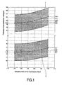
- an optical data storage medium which is characterized in that the spacer layer has a thickness selected from the range 20 - 30 ⁇ m, the thickness d TS0 in dependence on the refractive index n TS0 is within the upper shaded area in Fig.1 and the thickness d TS1 in dependence on the refractive index n TS1 is within the lower shaded area in Fig.1.
- the specifications of the Transmission Stacks (TS) include all possible layers on top of the concerning recording stack, such as e.g. gluing layers in case of foils, the spacer layer and the semi-transparent recording stack of L1 in case of TS0, the Cover Layer and possibly a Protective coating).
- EP-A-104705 5 it is known to use a polymer layer such as, for example, a polycarbonate (PC) sheet as light-transmissive cover or spacer layer and adhere such layer to the information storage layer by means of a thin, spin-coated layer of a UV curable liquid resin or a pressure sensitive adhesive (PSA).
- a polymer layer such as, for example, a polycarbonate (PC) sheet
- PC polycarbonate
- PSA pressure sensitive adhesive
- the spacer layer thickness or the amount of separation of the first information and the second information layer depends on the size of the photo-detector in the optical pick-up unit (OPU) of the optical medium drive, the magnification from the photo-detector to the medium, the reflectivity ratio of the first and second information layers and the distance between the two layers, i.e. the thickness of the spacer layer.
- OPU optical pick-up unit
- the maximum deviations of d TS0 and d TS1 from respectively the average values of d TS0 and d TS1 between a radius of 23 mm and 24 mm of the medium do not exceed ⁇ 2 ⁇ m measured over the whole area of the medium.
- n TS0 and n TS1 both have a value of 1.6 and the following conditions are fullfilled: 95 ⁇ m ⁇ d TS0 ⁇ 105 ⁇ m and 70 ⁇ m ⁇ d TS1 ⁇ 80 ⁇ m.
- Most plastic materials used as transparent layers have a refractive index of 1.6 or substantially close hereto. In this case reliable read out is possible when the thicknesses fall within the mentioned ranges.
- one method of manufacture comprises the application of a pressure sensitive adhesive (PSA) with a predetermined thickness which is UV-cured after being brought in contact with other layers of the medium.
- PSA pressure sensitive adhesive
- This material is usually supplied as a sheet of foil with the PSA on one or sides and those sheets are made with a predetermined thickness.
- Fig.1 the allowed thickness ranges of TS0 and TS1 are indicated
- the thickness d TS0 in dependence on the refractive index n TS0 is within the upper shaded area 1 and the thickness d TS1 in dependence on the refractive index n TS1 is within the lower shaded area 2.
- the spacer layer 24 (Fig. 2) has a thickness selected from the range 20 - 30 ⁇ m.
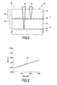
- FIG.2 an embodiment of the dual-stack optical data storage medium 20 according to the invention is shown.
- a focused laser beam 29 with a wavelength ⁇ of 405 nm and an Numerical Aperture (NA) of 0.85 enters through entrance face 26 of the medium 20 during read out.
- a substrate 21 made of polycarbonate has present on a side thereof: a first stack of layers 22 named L0 comprising a first information layer, a second stack of layers 23 named L1, comprising a second information layer.
- L1 is present at a position closest to the entrance face 26 and L0 is present more remote from the entrance face 26 than L1.
- a transparent cover layer 25 is present between the entrance face 26 and L1 and may be made of the same material or a sheet of PC or PMMA with a pressure sensitive adhesive (PSA).
- PSD pressure sensitive adhesive
- the spacer layer may also be a sheet combined with PSA.
- the L1 stack 23 has a relatively low thickness of a maimally a few hundred nm the influence of which may be neglected. Naturally L1 does affect the optical transmission but this aspect is not dealt with here.
- the transmission stack named TS1 has a thickness d TS1 of 75 ⁇ m and an effective refractive index n TS1 of 1.6 and contains all layers between L1 and the entrance face (26).
- the spacer layer (24) has a thickness of 25 ⁇ m.
- Fig. 3 the modeled data-to-clock jitter in %, when reading the first information layer of L0, as function of the stray-light from the out of focus layer, e.g. the second information layer of L1, is represented by graph 30.
- the jitter without stray-light was chosen to be 5.8%.
- the jitter has increased from 5.8% to 6.5% which is tolerable.
- Fig. 4 the ray-tracing simulation of the light reflected onto the photo-detector as function of the spacer-layer thickness is represented by graph 40.
- a 15% upper limit on the stray-light is represented by dotted line 41.
- the stray-light as function of the spacer- layer thickness was calculated for a OPU detector size of 100 ⁇ m and a magnification factor of 10.
- the minimum spacer layer 24 (Fig. 2) thickness to guarantee less than 15% stray-light is 20 ⁇ m.
- a dual-stack optical data storage medium for read out using a focused radiation beam with a wavelength of 400 - 410 nm and a Numerical Aperture (NA) of 0.84 - 0.86.
- the medium has a substrate and a first stack of layers named L0 comprising a first information layer and a second stack of layers named L1, comprising a second information layer.
- a radiation beam transparent spacer layer is present between L0 and L1.
- a transmission stack named TS0 with a thickness d TS0 and an effective refractive index n TS0 contains all layers between L0 and an entrance face of the medium.
- the spacer layer has a thickness selected from the range 20 - 30 ⁇ m, the thickness d TS0 in dependence on the refractive index n TS0 and the thickness d TS1 in dependence on the refractive index n TS0 are within a specified area. In this way a reliable read out of both the first and the second information layer of respectively L0 and L1 is achieved.
Landscapes
- Optical Record Carriers And Manufacture Thereof (AREA)
- Optical Recording Or Reproduction (AREA)
- Holo Graphy (AREA)
- Liquid Crystal (AREA)
- Optical Integrated Circuits (AREA)
- Automatic Disk Changers (AREA)
Claims (5)
- Optisches Datenspeichermedium mit zwei Schichtenfolgen (Dual-Stack-Datenspeichermedium) (20) zumindest zum Auslesen, bei dem ein fokussiertes Strahlenbündel (29) mit einer Wellenlänge λ zwischen 400 nm und 410 nm sowie eine numerische Apertur (NA) zwischen 0,84 und 0,86 verwendet werden, wobei das Strahlenbündel während des Auslesens durch eine Eintrittsfläche (26) des Mediums (20) eintritt und das Medium Folgendes umfasst:- ein Substrat (21) , auf dessen einer Seite Folgendes vorhanden ist:- eine erste Schichtenfolge (L0, 22), die eine erste Informationsschicht umfasst,- eine zweite Schichtenfolge (L1, 23), die eine zweite Informationsschicht umfasst, wobei sich die zweite Schichtenfolge (L1, 23) in einer der Eintrittsfläche (26) am nächsten gelegenen Position befindet und die erste Schichtenfolge (L0, 22) von der Eintrittsfläche (26) weiter entfernt ist als die zweite Schichtenfolge (L1, 23),- eine für das Strahlenbündel (29) transparente Abstandsschicht (24) zwischen der ersten Schichtenfolge (L0, 22) und der zweiten Schichtenfolge (L1, 23),- eine für das Strahlenbündel (29) transparente Deckschicht (25) zwischen der Eintrittsfläche (26) und der zweiten Schichtenfolge (L1, 23),- eine Übertragungsschichtenfolge TS0 mit einer Dicke DTS0 und einem effektiven Brechungsindex nTS0, die alle Schichten zwischen der ersten Schichtenfolge (L0, 22) und der Eintrittsfläche (26) enthält,- eine Übertragungsschichtenfolge TS1 mit einer Dicke dTS1 und einem effektiven Brechungsindex nTS1, die alle Schichten zwischen der zweiten Schichtenfolge (L1, 23) und der Eintrittsfläche (26) enthält,dadurch gekennzeichnet, dass
die Abstandsschicht (24) eine Dicke hat, die aus dem Bereich 20 - 30 µm ausgewählt ist, die Dicke dTS0 in Abhängigkeit vom Brechungsindex nTS0 innerhalb des oberen schraffierten Bereiches in Figur 1 liegt und die Dicke dTS1 in Abhängigkeit vom Brechungsindex nTS1 innerhalb des unteren schraffierten Bereiches in Figur 1 liegt. - Optisches Datenspeichermedium (20) nach Anspruch 1, bei dem die Abweichungen von dTS0 und DTS1 von den Durchschnittswerten von dTS0 bzw. DTS1 zwischen einem Radius von 23 mm und 24 mm des Mediums (20) maximal ±2 µm betragen, gemessen über die gesamte Fläche des Mediums (20).
- Optisches Datenspeichermedium (20) nach Anspruch 1 oder 2, bei dem nTS0 und nTS1 jeweils einen Wert von 1,6 haben und die folgenden Bedingungen erfüllt sind: 95 µm ≤ dTS0 ≤ 105 µm und 70 µm ≤ dTS1 ≤ 80 µm.
- Optisches Datenspeichermedium (20) nach einem der Ansprüche 1 bis 3, bei dem die Dicke der Abstandsschicht (24) 25 µm beträgt oder im Wesentlichen nahe 25 µm liegt und die Dicke der Deckschicht (25) 75 µm beträgt oder nahe 75 µm liegt.
- Verwendung eines optischen Datenspeichermediums nach einem der vorhergehenden Ansprüche.
Priority Applications (4)
| Application Number | Priority Date | Filing Date | Title |
|---|---|---|---|
| EP03730434A EP1516323B1 (de) | 2002-06-14 | 2003-06-11 | Zweischichtiger optischer datenträger und gebrauch desselben |
| SI200330734T SI1516323T1 (sl) | 2002-06-14 | 2003-06-11 | Optično sredstvo z dvemi zaporedji plasti za shranjevanje podatkov in uporaba takšnega sredstva |
| EP06126799A EP1770698A1 (de) | 2002-06-14 | 2003-06-11 | Zweischichtiger optischer Datenträger und Gebrauch desselben |
| CY20071100429T CY1107587T1 (el) | 2002-06-14 | 2007-03-28 | Μεσo αποθηκευσεως οπτικων δεδομενων σε δυο στοιβες και η χρησιμοποιηση ενος τετοιου μεσου |
Applications Claiming Priority (4)
| Application Number | Priority Date | Filing Date | Title |
|---|---|---|---|
| EP02077441 | 2002-06-14 | ||
| EP02077441 | 2002-06-14 | ||
| EP03730434A EP1516323B1 (de) | 2002-06-14 | 2003-06-11 | Zweischichtiger optischer datenträger und gebrauch desselben |
| PCT/IB2003/002570 WO2003107338A1 (en) | 2002-06-14 | 2003-06-11 | Dual stack optical data storage medium and use of such medium |
Related Child Applications (1)
| Application Number | Title | Priority Date | Filing Date |
|---|---|---|---|
| EP06126799A Division EP1770698A1 (de) | 2002-06-14 | 2003-06-11 | Zweischichtiger optischer Datenträger und Gebrauch desselben |
Publications (2)
| Publication Number | Publication Date |
|---|---|
| EP1516323A1 EP1516323A1 (de) | 2005-03-23 |
| EP1516323B1 true EP1516323B1 (de) | 2007-01-03 |
Family
ID=29724514
Family Applications (2)
| Application Number | Title | Priority Date | Filing Date |
|---|---|---|---|
| EP06126799A Withdrawn EP1770698A1 (de) | 2002-06-14 | 2003-06-11 | Zweischichtiger optischer Datenträger und Gebrauch desselben |
| EP03730434A Expired - Lifetime EP1516323B1 (de) | 2002-06-14 | 2003-06-11 | Zweischichtiger optischer datenträger und gebrauch desselben |
Family Applications Before (1)
| Application Number | Title | Priority Date | Filing Date |
|---|---|---|---|
| EP06126799A Withdrawn EP1770698A1 (de) | 2002-06-14 | 2003-06-11 | Zweischichtiger optischer Datenträger und Gebrauch desselben |
Country Status (17)
| Country | Link |
|---|---|
| US (1) | US20050207326A1 (de) |
| EP (2) | EP1770698A1 (de) |
| JP (1) | JP4342439B2 (de) |
| KR (1) | KR100987660B1 (de) |
| CN (2) | CN101127223A (de) |
| AT (1) | ATE350749T1 (de) |
| AU (1) | AU2003241114A1 (de) |
| CA (1) | CA2488825C (de) |
| CY (1) | CY1107587T1 (de) |
| DE (1) | DE60310933T2 (de) |
| DK (1) | DK1516323T3 (de) |
| ES (1) | ES2279116T3 (de) |
| MX (1) | MXPA04012118A (de) |
| PT (1) | PT1516323E (de) |
| SI (1) | SI1516323T1 (de) |
| TW (2) | TWI369679B (de) |
| WO (1) | WO2003107338A1 (de) |
Families Citing this family (10)
| Publication number | Priority date | Publication date | Assignee | Title |
|---|---|---|---|---|
| US9029028B2 (en) | 2003-12-29 | 2015-05-12 | Honeywell International Inc. | Hydrogen and electrical power generator |
| JP4341505B2 (ja) * | 2004-08-19 | 2009-10-07 | ソニー株式会社 | 多層光情報記録媒体 |
| JP2006164366A (ja) * | 2004-12-06 | 2006-06-22 | Toshiba Corp | 光ディスク、光ディスク装置、光ディスク再生方法 |
| US20060179448A1 (en) * | 2004-12-23 | 2006-08-10 | Smith Wayne M | Multilayer dual optical disk |
| US7976971B2 (en) | 2006-05-11 | 2011-07-12 | Honeywell International Inc. | Power generator with a pneumatic slide valve |
| US7713653B2 (en) | 2006-10-06 | 2010-05-11 | Honeywell International Inc. | Power generation capacity indicator |
| JPWO2010013441A1 (ja) * | 2008-07-31 | 2012-01-05 | パナソニック株式会社 | 光情報記録媒体及び記録再生装置 |
| US8932780B2 (en) | 2008-12-15 | 2015-01-13 | Honeywell International Inc. | Fuel cell |
| US9276285B2 (en) | 2008-12-15 | 2016-03-01 | Honeywell International Inc. | Shaped fuel source and fuel cell |
| US8246796B2 (en) | 2010-02-12 | 2012-08-21 | Honeywell International Inc. | Fuel cell recharger |
Family Cites Families (9)
| Publication number | Priority date | Publication date | Assignee | Title |
|---|---|---|---|---|
| JPH10302310A (ja) * | 1997-04-25 | 1998-11-13 | Sony Corp | 光学記録媒体及び光学ディスク装置 |
| KR100662671B1 (ko) * | 1999-10-04 | 2007-01-02 | 코닌클리케 필립스 일렉트로닉스 엔.브이. | 게르마늄-안티몬-텔루르 기록층을 구비한 광 기록매체 |
| ES2548717T3 (es) * | 2000-02-23 | 2015-10-20 | Koninklijke Philips N.V. | Medio de almacenamiento de datos regrabable |
| JP2001307381A (ja) * | 2000-04-24 | 2001-11-02 | Sony Corp | 光学記録媒体 |
| TW575873B (en) * | 2000-07-13 | 2004-02-11 | Matsushita Electric Industrial Co Ltd | Information recording medium, method for producing the same, and recording/reproducing method using the same |
| CN1312687C (zh) * | 2000-10-03 | 2007-04-25 | 松下电器产业株式会社 | 光学信息记录媒质,光学信息记录/再现方法和装置 |
| ATE395695T1 (de) * | 2000-10-27 | 2008-05-15 | Koninkl Philips Electronics Nv | Optische abtastvorrichtung |
| US7133331B2 (en) * | 2000-12-28 | 2006-11-07 | Victor Company Of Japan, Limited | Recording medium having a substrate containing microscopic pattern of parallel groove and land sections and recording/reproducing equipment therefor |
| CN1352456A (zh) * | 2001-11-30 | 2002-06-05 | 清华大学 | 具有多层可重写相变记录层的多层多阶光盘 |
-
2003
- 2003-06-11 TW TW096114812A patent/TWI369679B/zh not_active IP Right Cessation
- 2003-06-11 CA CA2488825A patent/CA2488825C/en not_active Expired - Lifetime
- 2003-06-11 WO PCT/IB2003/002570 patent/WO2003107338A1/en not_active Ceased
- 2003-06-11 AU AU2003241114A patent/AU2003241114A1/en not_active Abandoned
- 2003-06-11 CN CNA2007100018842A patent/CN101127223A/zh active Pending
- 2003-06-11 DK DK03730434T patent/DK1516323T3/da active
- 2003-06-11 US US10/517,472 patent/US20050207326A1/en not_active Abandoned
- 2003-06-11 PT PT03730434T patent/PT1516323E/pt unknown
- 2003-06-11 DE DE60310933T patent/DE60310933T2/de not_active Expired - Lifetime
- 2003-06-11 KR KR1020047020246A patent/KR100987660B1/ko not_active Expired - Lifetime
- 2003-06-11 CN CNB038133628A patent/CN100444261C/zh not_active Expired - Lifetime
- 2003-06-11 SI SI200330734T patent/SI1516323T1/sl unknown
- 2003-06-11 JP JP2004514069A patent/JP4342439B2/ja not_active Expired - Lifetime
- 2003-06-11 MX MXPA04012118A patent/MXPA04012118A/es active IP Right Grant
- 2003-06-11 ES ES03730434T patent/ES2279116T3/es not_active Expired - Lifetime
- 2003-06-11 TW TW092115859A patent/TWI303815B/zh not_active IP Right Cessation
- 2003-06-11 EP EP06126799A patent/EP1770698A1/de not_active Withdrawn
- 2003-06-11 EP EP03730434A patent/EP1516323B1/de not_active Expired - Lifetime
- 2003-06-11 AT AT03730434T patent/ATE350749T1/de active
-
2007
- 2007-03-28 CY CY20071100429T patent/CY1107587T1/el unknown
Also Published As
| Publication number | Publication date |
|---|---|
| EP1516323A1 (de) | 2005-03-23 |
| ES2279116T3 (es) | 2007-08-16 |
| JP2005530290A (ja) | 2005-10-06 |
| TWI303815B (en) | 2008-12-01 |
| CN100444261C (zh) | 2008-12-17 |
| JP4342439B2 (ja) | 2009-10-14 |
| CA2488825A1 (en) | 2003-12-24 |
| DE60310933T2 (de) | 2007-10-25 |
| AU2003241114A1 (en) | 2003-12-31 |
| KR100987660B1 (ko) | 2010-10-13 |
| ATE350749T1 (de) | 2007-01-15 |
| TW200406748A (en) | 2004-05-01 |
| US20050207326A1 (en) | 2005-09-22 |
| CY1107587T1 (el) | 2013-03-13 |
| CN101127223A (zh) | 2008-02-20 |
| EP1770698A1 (de) | 2007-04-04 |
| MXPA04012118A (es) | 2005-04-19 |
| TW200746129A (en) | 2007-12-16 |
| PT1516323E (pt) | 2007-04-30 |
| WO2003107338A1 (en) | 2003-12-24 |
| DK1516323T3 (da) | 2007-05-14 |
| TWI369679B (en) | 2012-08-01 |
| CA2488825C (en) | 2012-04-10 |
| SI1516323T1 (sl) | 2007-06-30 |
| DE60310933D1 (de) | 2007-02-15 |
| CN1659644A (zh) | 2005-08-24 |
| KR20050016549A (ko) | 2005-02-21 |
Similar Documents
| Publication | Publication Date | Title |
|---|---|---|
| US7172797B2 (en) | Optical information medium and a method of manufacturing the medium | |
| EP1516323B1 (de) | Zweischichtiger optischer datenträger und gebrauch desselben | |
| KR100661898B1 (ko) | 광디스크 장치 | |
| JP4267581B2 (ja) | 光記録媒体 | |
| JP4598021B2 (ja) | 光情報記録媒体 | |
| US20050232126A1 (en) | Optical data storage medium and use of such medium | |
| US20050163023A1 (en) | Optical data storage medium | |
| KR20050020991A (ko) | 광 데이터 저장매체와 이 매체의 용도 | |
| WO2007080925A1 (ja) | 光ピックアップ装置および当該光ピックアップ装置を備えた情報処理装置 | |
| HK1059140B (en) | Method of manufacturing an optical information medium | |
| JP2006525617A (ja) | 光記憶媒体 |
Legal Events
| Date | Code | Title | Description |
|---|---|---|---|
| PUAI | Public reference made under article 153(3) epc to a published international application that has entered the european phase |
Free format text: ORIGINAL CODE: 0009012 |
|
| 17P | Request for examination filed |
Effective date: 20050114 |
|
| AK | Designated contracting states |
Kind code of ref document: A1 Designated state(s): AT BE BG CH CY CZ DE DK EE ES FI FR GB GR HU IE IT LI LU MC NL PT RO SE SI SK TR |
|
| AX | Request for extension of the european patent |
Extension state: AL LT LV MK |
|
| DAX | Request for extension of the european patent (deleted) | ||
| GRAP | Despatch of communication of intention to grant a patent |
Free format text: ORIGINAL CODE: EPIDOSNIGR1 |
|
| GRAS | Grant fee paid |
Free format text: ORIGINAL CODE: EPIDOSNIGR3 |
|
| GRAA | (expected) grant |
Free format text: ORIGINAL CODE: 0009210 |
|
| AK | Designated contracting states |
Kind code of ref document: B1 Designated state(s): AT BE BG CH CY CZ DE DK EE ES FI FR GB GR HU IE IT LI LU MC NL PT RO SE SI SK TR |
|
| REG | Reference to a national code |
Ref country code: GB Ref legal event code: FG4D |
|
| REF | Corresponds to: |
Ref document number: 60310933 Country of ref document: DE Date of ref document: 20070215 Kind code of ref document: P |
|
| REG | Reference to a national code |
Ref country code: IE Ref legal event code: FG4D |
|
| REG | Reference to a national code |
Ref country code: RO Ref legal event code: EPE |
|
| REG | Reference to a national code |
Ref country code: SE Ref legal event code: TRGR |
|
| REG | Reference to a national code |
Ref country code: GR Ref legal event code: EP Ref document number: 20070401000 Country of ref document: GR |
|
| REG | Reference to a national code |
Ref country code: PT Ref legal event code: SC4A Free format text: AVAILABILITY OF NATIONAL TRANSLATION Effective date: 20070328 |
|
| REG | Reference to a national code |
Ref country code: DK Ref legal event code: T3 |
|
| REG | Reference to a national code |
Ref country code: HU Ref legal event code: AG4A Ref document number: E001461 Country of ref document: HU |
|
| REG | Reference to a national code |
Ref country code: EE Ref legal event code: FG4A Ref document number: E001125 Country of ref document: EE Effective date: 20070402 |
|
| ET | Fr: translation filed | ||
| REG | Reference to a national code |
Ref country code: ES Ref legal event code: FG2A Ref document number: 2279116 Country of ref document: ES Kind code of ref document: T3 |
|
| PLBE | No opposition filed within time limit |
Free format text: ORIGINAL CODE: 0009261 |
|
| STAA | Information on the status of an ep patent application or granted ep patent |
Free format text: STATUS: NO OPPOSITION FILED WITHIN TIME LIMIT |
|
| 26N | No opposition filed |
Effective date: 20071005 |
|
| REG | Reference to a national code |
Ref country code: ES Ref legal event code: PC2A Owner name: KONINKLIJKE PHILIPS N.V. Effective date: 20140221 |
|
| REG | Reference to a national code |
Ref country code: DE Ref legal event code: R082 Ref document number: 60310933 Country of ref document: DE Representative=s name: VOLMER, GEORG, DIPL.-ING., DE |
|
| REG | Reference to a national code |
Ref country code: DE Ref legal event code: R082 Ref document number: 60310933 Country of ref document: DE Representative=s name: VOLMER, GEORG, DIPL.-ING., DE Effective date: 20140328 Ref country code: DE Ref legal event code: R081 Ref document number: 60310933 Country of ref document: DE Owner name: KONINKLIJKE PHILIPS N.V., NL Free format text: FORMER OWNER: KONINKLIJKE PHILIPS ELECTRONICS N.V., EINDHOVEN, NL Effective date: 20140328 Ref country code: DE Ref legal event code: R082 Ref document number: 60310933 Country of ref document: DE Representative=s name: MEISSNER, BOLTE & PARTNER GBR, DE Effective date: 20140328 Ref country code: DE Ref legal event code: R082 Ref document number: 60310933 Country of ref document: DE Representative=s name: MEISSNER BOLTE PATENTANWAELTE RECHTSANWAELTE P, DE Effective date: 20140328 |
|
| REG | Reference to a national code |
Ref country code: FR Ref legal event code: CA Effective date: 20141126 Ref country code: FR Ref legal event code: CD Owner name: KONINKLIJKE PHILIPS N.V., NL Effective date: 20141126 |
|
| REG | Reference to a national code |
Ref country code: DE Ref legal event code: R082 Ref document number: 60310933 Country of ref document: DE Representative=s name: MEISSNER, BOLTE & PARTNER GBR, DE Ref country code: DE Ref legal event code: R082 Ref document number: 60310933 Country of ref document: DE Representative=s name: MEISSNER BOLTE PATENTANWAELTE RECHTSANWAELTE P, DE |
|
| REG | Reference to a national code |
Ref country code: FR Ref legal event code: PLFP Year of fee payment: 14 |
|
| REG | Reference to a national code |
Ref country code: FR Ref legal event code: PLFP Year of fee payment: 15 |
|
| REG | Reference to a national code |
Ref country code: FR Ref legal event code: PLFP Year of fee payment: 16 |
|
| PGFP | Annual fee paid to national office [announced via postgrant information from national office to epo] |
Ref country code: IE Payment date: 20190624 Year of fee payment: 17 Ref country code: LU Payment date: 20190626 Year of fee payment: 17 Ref country code: FI Payment date: 20190620 Year of fee payment: 17 Ref country code: MC Payment date: 20190624 Year of fee payment: 17 |
|
| PGFP | Annual fee paid to national office [announced via postgrant information from national office to epo] |
Ref country code: TR Payment date: 20190531 Year of fee payment: 17 Ref country code: TR Payment date: 20190528 Year of fee payment: 17 Ref country code: HU Payment date: 20190607 Year of fee payment: 17 Ref country code: BE Payment date: 20190625 Year of fee payment: 17 Ref country code: EE Payment date: 20190627 Year of fee payment: 17 Ref country code: SI Payment date: 20190604 Year of fee payment: 17 Ref country code: GR Payment date: 20190628 Year of fee payment: 17 |
|
| PGFP | Annual fee paid to national office [announced via postgrant information from national office to epo] |
Ref country code: SK Payment date: 20190530 Year of fee payment: 17 |
|
| PGFP | Annual fee paid to national office [announced via postgrant information from national office to epo] |
Ref country code: AT Payment date: 20190621 Year of fee payment: 17 |
|
| PGFP | Annual fee paid to national office [announced via postgrant information from national office to epo] |
Ref country code: BG Payment date: 20190626 Year of fee payment: 17 |
|
| REG | Reference to a national code |
Ref country code: FI Ref legal event code: MAE |
|
| REG | Reference to a national code |
Ref country code: EE Ref legal event code: MM4A Ref document number: E001125 Country of ref document: EE Effective date: 20200630 |
|
| PG25 | Lapsed in a contracting state [announced via postgrant information from national office to epo] |
Ref country code: PT Free format text: LAPSE BECAUSE OF NON-PAYMENT OF DUE FEES Effective date: 20201211 Ref country code: FI Free format text: LAPSE BECAUSE OF NON-PAYMENT OF DUE FEES Effective date: 20200611 Ref country code: MC Free format text: LAPSE BECAUSE OF NON-PAYMENT OF DUE FEES Effective date: 20200630 Ref country code: RO Free format text: LAPSE BECAUSE OF NON-PAYMENT OF DUE FEES Effective date: 20200611 |
|
| REG | Reference to a national code |
Ref country code: SK Ref legal event code: MM4A Ref document number: E 1561 Country of ref document: SK Effective date: 20200611 |
|
| REG | Reference to a national code |
Ref country code: AT Ref legal event code: MM01 Ref document number: 350749 Country of ref document: AT Kind code of ref document: T Effective date: 20200611 |
|
| PG25 | Lapsed in a contracting state [announced via postgrant information from national office to epo] |
Ref country code: LU Free format text: LAPSE BECAUSE OF NON-PAYMENT OF DUE FEES Effective date: 20200611 |
|
| REG | Reference to a national code |
Ref country code: BE Ref legal event code: MM Effective date: 20200630 |
|
| PG25 | Lapsed in a contracting state [announced via postgrant information from national office to epo] |
Ref country code: HU Free format text: LAPSE BECAUSE OF NON-PAYMENT OF DUE FEES Effective date: 20200612 Ref country code: GR Free format text: LAPSE BECAUSE OF NON-PAYMENT OF DUE FEES Effective date: 20210111 Ref country code: IE Free format text: LAPSE BECAUSE OF NON-PAYMENT OF DUE FEES Effective date: 20200611 Ref country code: EE Free format text: LAPSE BECAUSE OF NON-PAYMENT OF DUE FEES Effective date: 20200630 Ref country code: PT Free format text: LAPSE BECAUSE OF NON-PAYMENT OF DUE FEES Effective date: 20210114 |
|
| REG | Reference to a national code |
Ref country code: SI Ref legal event code: KO00 Effective date: 20210317 |
|
| PG25 | Lapsed in a contracting state [announced via postgrant information from national office to epo] |
Ref country code: SI Free format text: LAPSE BECAUSE OF NON-PAYMENT OF DUE FEES Effective date: 20200612 Ref country code: BE Free format text: LAPSE BECAUSE OF NON-PAYMENT OF DUE FEES Effective date: 20200630 Ref country code: AT Free format text: LAPSE BECAUSE OF NON-PAYMENT OF DUE FEES Effective date: 20200611 Ref country code: BG Free format text: LAPSE BECAUSE OF NON-PAYMENT OF DUE FEES Effective date: 20201231 |
|
| PG25 | Lapsed in a contracting state [announced via postgrant information from national office to epo] |
Ref country code: SK Free format text: LAPSE BECAUSE OF NON-PAYMENT OF DUE FEES Effective date: 20200611 |
|
| PG25 | Lapsed in a contracting state [announced via postgrant information from national office to epo] |
Ref country code: TR Free format text: LAPSE BECAUSE OF NON-PAYMENT OF DUE FEES Effective date: 20200611 |
|
| PGFP | Annual fee paid to national office [announced via postgrant information from national office to epo] |
Ref country code: SE Payment date: 20220622 Year of fee payment: 20 Ref country code: NL Payment date: 20220627 Year of fee payment: 20 Ref country code: IT Payment date: 20220622 Year of fee payment: 20 Ref country code: GB Payment date: 20220621 Year of fee payment: 20 Ref country code: DK Payment date: 20220627 Year of fee payment: 20 Ref country code: CZ Payment date: 20220610 Year of fee payment: 20 |
|
| PGFP | Annual fee paid to national office [announced via postgrant information from national office to epo] |
Ref country code: FR Payment date: 20220624 Year of fee payment: 20 |
|
| PGFP | Annual fee paid to national office [announced via postgrant information from national office to epo] |
Ref country code: ES Payment date: 20220712 Year of fee payment: 20 Ref country code: DE Payment date: 20220628 Year of fee payment: 20 Ref country code: CY Payment date: 20220610 Year of fee payment: 20 |
|
| PGFP | Annual fee paid to national office [announced via postgrant information from national office to epo] |
Ref country code: CH Payment date: 20220628 Year of fee payment: 20 |
|
| REG | Reference to a national code |
Ref country code: DE Ref legal event code: R071 Ref document number: 60310933 Country of ref document: DE |
|
| REG | Reference to a national code |
Ref country code: DK Ref legal event code: EUP Expiry date: 20230611 |
|
| REG | Reference to a national code |
Ref country code: NL Ref legal event code: MK Effective date: 20230610 |
|
| REG | Reference to a national code |
Ref country code: CH Ref legal event code: PL |
|
| REG | Reference to a national code |
Ref country code: ES Ref legal event code: FD2A Effective date: 20230626 |
|
| REG | Reference to a national code |
Ref country code: GB Ref legal event code: PE20 Expiry date: 20230610 |
|
| PG25 | Lapsed in a contracting state [announced via postgrant information from national office to epo] |
Ref country code: ES Free format text: LAPSE BECAUSE OF EXPIRATION OF PROTECTION Effective date: 20230612 Ref country code: CZ Free format text: LAPSE BECAUSE OF EXPIRATION OF PROTECTION Effective date: 20230611 |
|
| REG | Reference to a national code |
Ref country code: SE Ref legal event code: EUG |
|
| PG25 | Lapsed in a contracting state [announced via postgrant information from national office to epo] |
Ref country code: GB Free format text: LAPSE BECAUSE OF EXPIRATION OF PROTECTION Effective date: 20230610 |