EP1517189A2 - Optimierung einer kritischen Dimension in der Lithographie - Google Patents
Optimierung einer kritischen Dimension in der Lithographie Download PDFInfo
- Publication number
- EP1517189A2 EP1517189A2 EP04255674A EP04255674A EP1517189A2 EP 1517189 A2 EP1517189 A2 EP 1517189A2 EP 04255674 A EP04255674 A EP 04255674A EP 04255674 A EP04255674 A EP 04255674A EP 1517189 A2 EP1517189 A2 EP 1517189A2
- Authority
- EP
- European Patent Office
- Prior art keywords
- exposure
- substrates
- substrate
- attributes
- corrective
- Prior art date
- Legal status (The legal status is an assumption and is not a legal conclusion. Google has not performed a legal analysis and makes no representation as to the accuracy of the status listed.)
- Withdrawn
Links
- 238000001459 lithography Methods 0.000 title description 2
- 239000000758 substrate Substances 0.000 claims abstract description 126
- 238000000034 method Methods 0.000 claims abstract description 62
- 238000012545 processing Methods 0.000 claims abstract description 48
- 238000012937 correction Methods 0.000 claims abstract description 44
- 230000001105 regulatory effect Effects 0.000 claims abstract description 4
- 230000008569 process Effects 0.000 claims description 39
- 230000007246 mechanism Effects 0.000 claims description 28
- 238000004364 calculation method Methods 0.000 claims description 17
- 230000008859 change Effects 0.000 claims description 8
- 230000003044 adaptive effect Effects 0.000 claims description 7
- 238000012544 monitoring process Methods 0.000 claims description 6
- 230000000977 initiatory effect Effects 0.000 claims 3
- 238000004590 computer program Methods 0.000 claims 1
- 235000012431 wafers Nutrition 0.000 description 95
- 238000005259 measurement Methods 0.000 description 15
- 230000005855 radiation Effects 0.000 description 14
- 230000000875 corresponding effect Effects 0.000 description 12
- 239000010410 layer Substances 0.000 description 9
- 238000000059 patterning Methods 0.000 description 6
- 238000004519 manufacturing process Methods 0.000 description 5
- XUIMIQQOPSSXEZ-UHFFFAOYSA-N Silicon Chemical compound [Si] XUIMIQQOPSSXEZ-UHFFFAOYSA-N 0.000 description 4
- 238000004140 cleaning Methods 0.000 description 4
- 238000005530 etching Methods 0.000 description 4
- 238000005468 ion implantation Methods 0.000 description 4
- 238000001465 metallisation Methods 0.000 description 4
- 230000003647 oxidation Effects 0.000 description 4
- 238000007254 oxidation reaction Methods 0.000 description 4
- 238000005498 polishing Methods 0.000 description 4
- 229910052710 silicon Inorganic materials 0.000 description 4
- 239000010703 silicon Substances 0.000 description 4
- 230000002596 correlated effect Effects 0.000 description 3
- 238000010586 diagram Methods 0.000 description 3
- 238000010884 ion-beam technique Methods 0.000 description 3
- 239000006117 anti-reflective coating Substances 0.000 description 2
- 239000011248 coating agent Substances 0.000 description 2
- 238000000576 coating method Methods 0.000 description 2
- 230000007547 defect Effects 0.000 description 2
- 238000009826 distribution Methods 0.000 description 2
- 238000007689 inspection Methods 0.000 description 2
- 239000000463 material Substances 0.000 description 2
- 238000012986 modification Methods 0.000 description 2
- 230000004048 modification Effects 0.000 description 2
- 230000010363 phase shift Effects 0.000 description 2
- 238000012805 post-processing Methods 0.000 description 2
- 238000007781 pre-processing Methods 0.000 description 2
- 241000136406 Comones Species 0.000 description 1
- 238000003491 array Methods 0.000 description 1
- 230000002238 attenuated effect Effects 0.000 description 1
- 230000006399 behavior Effects 0.000 description 1
- 230000005540 biological transmission Effects 0.000 description 1
- 230000003750 conditioning effect Effects 0.000 description 1
- 238000010276 construction Methods 0.000 description 1
- 230000001276 controlling effect Effects 0.000 description 1
- 238000013461 design Methods 0.000 description 1
- 238000001514 detection method Methods 0.000 description 1
- 238000011161 development Methods 0.000 description 1
- 230000000694 effects Effects 0.000 description 1
- 230000005670 electromagnetic radiation Effects 0.000 description 1
- 238000010894 electron beam technology Methods 0.000 description 1
- 239000010408 film Substances 0.000 description 1
- 238000005286 illumination Methods 0.000 description 1
- 238000003384 imaging method Methods 0.000 description 1
- 230000006872 improvement Effects 0.000 description 1
- 230000001678 irradiating effect Effects 0.000 description 1
- 238000012804 iterative process Methods 0.000 description 1
- 239000002346 layers by function Substances 0.000 description 1
- 239000004973 liquid crystal related substance Substances 0.000 description 1
- 230000005381 magnetic domain Effects 0.000 description 1
- 239000011159 matrix material Substances 0.000 description 1
- 230000015654 memory Effects 0.000 description 1
- QSHDDOUJBYECFT-UHFFFAOYSA-N mercury Chemical compound [Hg] QSHDDOUJBYECFT-UHFFFAOYSA-N 0.000 description 1
- 229910052753 mercury Inorganic materials 0.000 description 1
- 230000003287 optical effect Effects 0.000 description 1
- 239000002245 particle Substances 0.000 description 1
- 230000037452 priming Effects 0.000 description 1
- 230000004044 response Effects 0.000 description 1
- 238000007493 shaping process Methods 0.000 description 1
- 239000010409 thin film Substances 0.000 description 1
- 238000012546 transfer Methods 0.000 description 1
- 238000012795 verification Methods 0.000 description 1
Images



Classifications
-
- G—PHYSICS
- G03—PHOTOGRAPHY; CINEMATOGRAPHY; ANALOGOUS TECHNIQUES USING WAVES OTHER THAN OPTICAL WAVES; ELECTROGRAPHY; HOLOGRAPHY
- G03F—PHOTOMECHANICAL PRODUCTION OF TEXTURED OR PATTERNED SURFACES, e.g. FOR PRINTING, FOR PROCESSING OF SEMICONDUCTOR DEVICES; MATERIALS THEREFOR; ORIGINALS THEREFOR; APPARATUS SPECIALLY ADAPTED THEREFOR
- G03F7/00—Photomechanical, e.g. photolithographic, production of textured or patterned surfaces, e.g. printing surfaces; Materials therefor, e.g. comprising photoresists; Apparatus specially adapted therefor
- G03F7/70—Microphotolithographic exposure; Apparatus therefor
- G03F7/708—Construction of apparatus, e.g. environment aspects, hygiene aspects or materials
- G03F7/70991—Connection with other apparatus, e.g. multiple exposure stations, particular arrangement of exposure apparatus and pre-exposure and/or post-exposure apparatus; Shared apparatus, e.g. having shared radiation source, shared mask or workpiece stage, shared base-plate; Utilities, e.g. cable, pipe or wireless arrangements for data, power, fluids or vacuum
-
- G—PHYSICS
- G03—PHOTOGRAPHY; CINEMATOGRAPHY; ANALOGOUS TECHNIQUES USING WAVES OTHER THAN OPTICAL WAVES; ELECTROGRAPHY; HOLOGRAPHY
- G03F—PHOTOMECHANICAL PRODUCTION OF TEXTURED OR PATTERNED SURFACES, e.g. FOR PRINTING, FOR PROCESSING OF SEMICONDUCTOR DEVICES; MATERIALS THEREFOR; ORIGINALS THEREFOR; APPARATUS SPECIALLY ADAPTED THEREFOR
- G03F7/00—Photomechanical, e.g. photolithographic, production of textured or patterned surfaces, e.g. printing surfaces; Materials therefor, e.g. comprising photoresists; Apparatus specially adapted therefor
- G03F7/70—Microphotolithographic exposure; Apparatus therefor
- G03F7/70483—Information management; Active and passive control; Testing; Wafer monitoring, e.g. pattern monitoring
- G03F7/70491—Information management, e.g. software; Active and passive control, e.g. details of controlling exposure processes or exposure tool monitoring processes
- G03F7/705—Modelling or simulating from physical phenomena up to complete wafer processes or whole workflow in wafer productions
-
- G—PHYSICS
- G03—PHOTOGRAPHY; CINEMATOGRAPHY; ANALOGOUS TECHNIQUES USING WAVES OTHER THAN OPTICAL WAVES; ELECTROGRAPHY; HOLOGRAPHY
- G03F—PHOTOMECHANICAL PRODUCTION OF TEXTURED OR PATTERNED SURFACES, e.g. FOR PRINTING, FOR PROCESSING OF SEMICONDUCTOR DEVICES; MATERIALS THEREFOR; ORIGINALS THEREFOR; APPARATUS SPECIALLY ADAPTED THEREFOR
- G03F7/00—Photomechanical, e.g. photolithographic, production of textured or patterned surfaces, e.g. printing surfaces; Materials therefor, e.g. comprising photoresists; Apparatus specially adapted therefor
- G03F7/70—Microphotolithographic exposure; Apparatus therefor
- G03F7/70483—Information management; Active and passive control; Testing; Wafer monitoring, e.g. pattern monitoring
- G03F7/7055—Exposure light control in all parts of the microlithographic apparatus, e.g. pulse length control or light interruption
- G03F7/70558—Dose control, i.e. achievement of a desired dose
-
- G—PHYSICS
- G03—PHOTOGRAPHY; CINEMATOGRAPHY; ANALOGOUS TECHNIQUES USING WAVES OTHER THAN OPTICAL WAVES; ELECTROGRAPHY; HOLOGRAPHY
- G03F—PHOTOMECHANICAL PRODUCTION OF TEXTURED OR PATTERNED SURFACES, e.g. FOR PRINTING, FOR PROCESSING OF SEMICONDUCTOR DEVICES; MATERIALS THEREFOR; ORIGINALS THEREFOR; APPARATUS SPECIALLY ADAPTED THEREFOR
- G03F7/00—Photomechanical, e.g. photolithographic, production of textured or patterned surfaces, e.g. printing surfaces; Materials therefor, e.g. comprising photoresists; Apparatus specially adapted therefor
- G03F7/70—Microphotolithographic exposure; Apparatus therefor
- G03F7/70483—Information management; Active and passive control; Testing; Wafer monitoring, e.g. pattern monitoring
- G03F7/70605—Workpiece metrology
- G03F7/70616—Monitoring the printed patterns
- G03F7/70625—Dimensions, e.g. line width, critical dimension [CD], profile, sidewall angle or edge roughness
-
- G—PHYSICS
- G03—PHOTOGRAPHY; CINEMATOGRAPHY; ANALOGOUS TECHNIQUES USING WAVES OTHER THAN OPTICAL WAVES; ELECTROGRAPHY; HOLOGRAPHY
- G03F—PHOTOMECHANICAL PRODUCTION OF TEXTURED OR PATTERNED SURFACES, e.g. FOR PRINTING, FOR PROCESSING OF SEMICONDUCTOR DEVICES; MATERIALS THEREFOR; ORIGINALS THEREFOR; APPARATUS SPECIALLY ADAPTED THEREFOR
- G03F7/00—Photomechanical, e.g. photolithographic, production of textured or patterned surfaces, e.g. printing surfaces; Materials therefor, e.g. comprising photoresists; Apparatus specially adapted therefor
- G03F7/70—Microphotolithographic exposure; Apparatus therefor
- G03F7/70691—Handling of masks or workpieces
- G03F7/707—Chucks, e.g. chucking or un-chucking operations or structural details
Definitions
- the present invention generally relates to lithographic systems and methods of lithographic exposure.
- patterning device as will be employed herein should be broadly interpreted to refer to devices that can be used to endow an incoming radiation beam with a patterned cross-section, corresponding to a pattern that is to be created in a target portion of the substrate.
- the term “light valve” may also be used in this context.
- the pattern will correspond to a particular functional layer in a device being created in the target portion, such as an integrated circuit or other device (see below). Examples of such patterning devices include:
- a mask the concept of a mask is well known in lithography, and it includes mask types such as binary, alternating phase-shift, and attenuated phase-shift, as well as various hybrid mask types. Placement of such a mask in the radiation beam causes selective transmission (in the case of a transmissive mask) or reflection (in the case of a reflective mask) of the radiation impinging on the mask, according to the pattern on the mask.
- the support structure will generally be a mask table, which ensures that the mask can be held at a desired position in the incoming radiation beam, and that it can be moved relative to the beam if so desired;
- a programmable mirror array an example of such a device is a matrix-addressable surface having a viscoelastic control layer and a reflective surface.
- the basic principle behind such an apparatus is that (for example) addressed areas of the reflective surface reflect incident light as diffracted light, whereas unaddressed areas reflect incident light as undiffracted light.
- the said undiffracted light can be filtered out of the reflected beam, leaving only the diffracted light behind; in this manner, the beam becomes patterned according to the addressing pattern of the matrix-addressable surface.
- the required matrix addressing can be performed using suitable electronic means. More information on such mirror arrays can be gleaned, for example, from United States Patent Nos.
- the said support structure may be embodied as a frame or table, for example, which may be fixed or movable as required;
- a programmable LCD array an example of such a construction is given in United States Patent No. US 5,229,872, which is incorporated herein by reference.
- the support structure in this case may be embodied as a frame or table, for example, which may be fixed or movable as required.
- the projection system may hereinafter be referred to as the "lens"; however, this term should be broadly interpreted as encompassing various types of projection system, including refractive optics, reflective optics, and catadioptric systems, for example.
- the radiation system may also include components operating according to any of these design types for directing, shaping or controlling the projection beam of radiation, and such components may also be referred to below, collectively or singularly, as a "lens".
- Lithographic exposure apparatuses can be used, for example, in the manufacture of integrated circuits (ICs).
- the patterning devices may generate a circuit pattern corresponding to an individual layer of the IC, and this pattern can be imaged onto a target portion (e.g. comprising one or more dies) on a substrate (silicon wafer) that has been coated with a layer of radiation-sensitive material (resist).
- a target portion e.g. comprising one or more dies
- substrate silicon wafer
- resist radiation-sensitive material
- a single wafer will contain a whole network of adjacent target portions that are successively irradiated via the projection system, one at a time.
- each target portion is irradiated by exposing the entire mask pattern onto the target portion in one go; such an apparatus is commonly referred to as a wafer stepper.
- a wafer stepper In an alternative apparatus - commonly referred to as a step-and-scan apparatus - each target portion is irradiated by progressively scanning the mask pattern under the projection beam in a given reference direction (the "scanning" direction) while synchronously scanning the substrate table parallel or anti-parallel to this direction.
- the projection system will have a magnification factor M (generally ⁇ 1)
- M magnification factor
- the speed V at which the substrate table is scanned will be a factor M times that at which the mask table is scanned.
- the lithographic apparatus may also be of a type having two or more substrate tables (and/or two or more mask tables). In such "multiple stage" devices the additional tables may be used in parallel, or preparatory steps may be carried out on one or more tables while one or more other tables are being used for exposures.
- Twin stage lithographic apparatus are described, for example, in United States Patent No. 5,969,441 and WO 98/40791, incorporated herein by reference.
- lithographic systems are used in the manufacture of integrated circuits (ICs). Such systems commonly employ a lithographic exposure apparatus and a wafer track apparatus.
- the lithographic exposure apparatus is configured to project or expose circuit pattern residing on a reticle (e.g., mask) onto a target field of a silicon wafer substrate layer via an irradiating projection beam.
- the projection beam may encompass different types of electromagnetic radiation including, but not limited to, ultraviolet radiation (UV) and extreme ultra-violet radiation (EUV), as well as particle beams, such as ion beams or electron beams.
- the silicon wafer layer is previously coated with radiation-sensitive material (e.g., resist) that interacts with the impinging projection beam to replicate the profile and features of the mask circuit pattern onto the wafer substrate target fields.
- radiation-sensitive material e.g., resist
- a single wafer layer will contain a entire network of adjacent target fields that are successively irradiated.
- steppers each target portion is irradiated by exposing the entire mask pattern onto the target portion at once.
- step-and-scan tools each target portion is irradiated by progressively scanning the mask circuit pattern under the projection beam in a given reference direction while synchronously scanning the substrate.
- the substrate may be subjected to a variety of processes before the exposure process.
- the substrate will generally be treated with resist before exposure.
- the substrate may be subjected to cleaning, etching, ion implantation (e.g., doping), metallization, oxidation, chemo-mechanical polishing, priming, resist coating, soft bake processes, , and measurement processes.
- the substrate may also be subjected to a series of post-exposure processes, such as, for example, post exposure bake (PEB), development, hard bake, etching, ion implantation (e.g., doping), metallization, oxidation, chemo-mechanical polishing, cleaning, and measurement processes.
- PEB post exposure bake
- etching ion implantation
- metallization oxidation
- chemo-mechanical polishing cleaning, and measurement processes.
- pre- and post-exposure processes are performed by stations or modules designed for their respective purposes.
- the substrate is subjected to these processing modules, as well as to the lithographic exposure apparatus, in a pre-defined sequence.
- the substrate wafers travel in a pre-specified processing path to get serviced by specific processing modules that can be tracked.
- the processing path can be monitored, recorded, controlled, and limited to specific paths.
- wafer track apparatus 104 interconnects lithographic exposure apparatus 102 with a multitude of pre-processing modules 104, 106 and post exposure processing modules 104, 108.
- the pre- and post-exposure processing modules 104, 106, 108 can be apparatus that are external to the wafer track apparatus or modules that are internal to the wafer track apparatus.
- the wafer track apparatus 104 may also include interface sections configured to transport the wafer substrates to and from lithographic exposure apparatus 102, pre-processing apparatus 106, post-processing apparatus 108, and transport the wafer substrates between the various processing modules internal to the wafer track apparatus 104.
- Pre-exposure processes external to the wafer track 106 may include, for example, cleaning, etching, ion implantation (e.g., doping), metallization, oxidation, chemo-mechanical polishing, and measurement apparatus.
- Pre-exposure process modules internal to the wafer track 104 may include, for example, wafer supply, resist coating, measurement, and soft bake modules.
- Post-processing modules internal to the wafer track 104 may include, for example, post-exposure bake (PEB), develop, hard bake, and measurement modules.
- Post-exposure processes external to the wafer track 108 may include, for example, cleaning, etching, ion implantation (e.g., doping), metallization, oxidation, chemo-mechanical polishing, and measurement apparatus.
- the CD may include, for example, the gap between features, X and/or Y diameter of holes and/or posts, ellipticity of holes and/or posts, area of feature, feature sidewall angle, width at the top of a feature, width at the middle of a feature, width at the bottom of a feature, and line edge roughness.
- CDU critical dimension uniformity
- PEB post exposure bake
- Systems, apparatuses and methods consistent with the principles of the present invention provide for the improvement of CD uniformity in a lithographic system that employs an exposure apparatus and a track apparatus.
- the invention measures the attributes of substrates processed by the lithographic system, assesses whether the processed substrates CDs are uniform based on pre-specified CD criteria and, in response to determining that the CDs are not uniform, corrective exposure data are adaptively calculated based on the measured CD attributes.
- the corrective exposure data is configured to correct non-uniformities in the substrates by regulating the exposure dosage in the exposure apparatus of the lithographic system.
- the substrates are then exposed by the exposure apparatus of the lithographic system in accordance with the corrective exposure data.
- FIG. 1A is a schematic illustration of a lithographic system
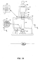
- FIG. 1B is a schematic illustration of a lithographic projection apparatus
- FIG. 2 is a high level flow diagram depicting an embodiment of the present invention
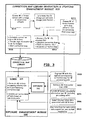
- FIG. 3 is a schematic functional block diagram depicting an embodiment of the present invention.
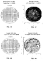
- FIGs. 4A, 4B illustrate examples of pre-exposure metrology data
- FIGs. 4C, 4D illustrate a typical dose layout used to determine the gain factor for the process and the corresponding wafer CD change per unit dose, respectively;
- FIGs. 4E, 4F illustrate a typical dose layout with dose offsets set to zero and the corresponding results of a wafer CD, respectively.
- FIGs. 4G, 4H illustrate a typical optimal corrected dose layout and the corresponding results of a wafer CD, respectively.
- processes that treat the substrate wafers contribute to variations in CDU that negatively affect the quality and performance of the exposed patterns.
- Such non-uniformities may occur across a target field, across a wafer, and between wafers.
- these non-uniformities can also vary depending a variety of factors, such as the particular path the substrate wafer travels, scheduling anomalies, etc.
- the present invention contemplates a lithographic system that employs an adaptive CD enhancement process whereby these variations and non-uniformities are factored out to provide acceptable CDU levels.
- Such a process exploits information regarding the lithographic system, for example, wafer track processing data, metrology data, and/or substrate wafer history data, to iteratively arrive at and maintain the optimal corrective dose offsets that improve overall CDU performance.
- FIG. 1A schematically depicts lithographic system 100 according to a particular embodiment of the invention.
- System 100 comprises lithographic exposure apparatus 102, which is configured to expose a pattern onto a substrate wafer, and wafer track apparatus 104, which is configured to transport the substrate wafers between the various pre- and post-exposure processing modules.
- FIG. 1B provides a more detailed illustration of lithographic apparatus 102.
- lithographic apparatus 102 includes radiation source LA and radiation system IL for providing a projection beam PB, a first object table (e.g. mask table) MT provided with a mask holder for holding a mask MA (e.g. a reticle), and a projection system PL ( e.g., lens) for imaging an irradiated portion of the mask MA onto a target portion C (e.g. comprising one or more dies) of the substrate W.
- lithographic apparatus 102 is of a transmissive type (i.e. has a transmissive mask). However, in general, it may also be of a reflective type, for example (with a reflective mask) and, alternatively, apparatus 102 may employ another kind of patterning devices, such as a programmable mirror array of a type as indicated above.
- Lithographic apparatus 102 further comprises a second object table (e.g. , substrate table) WT provided with a substrate holder for holding a substrate W (e.g. a resist-coated silicon wafer).
- a second object table e.g. , substrate table
- WT e.g. a resist-coated silicon wafer
- Source LA produces a beam of radiation, which is fed into illumination system (e.g. , illuminator) IL, either directly or after having traversed conditioning mechanisms , such as a beam expander EX , for example.
- Illuminator IL may comprise adjusting mechanism AM for setting the outer and/or inner radial extent (commonly referred to as ⁇ -outer and ⁇ -inner, respectively) of the intensity distribution in the beam.
- ⁇ -outer and ⁇ -inner respectively
- it will generally comprise various other components, such as an integrator IN and a condenser CO.
- the beam PB impinging on the mask MA has a desired cross-sectional uniformity and intensity distribution.
- source LA may be within the housing of lithographic exposure apparatus 102 (as is often the case when the source LA is a mercury lamp, for example). However, it may also be remote from apparatus 102, as in the case of an excimer laser source. In this scenario, the remote radiation beam is guided into apparatus 102 by virtue of suitable directing mirrors.
- the beam PB subsequently intercepts the mask MA, which is held on a mask table MT. Having traversed the mask MA, the beam PB passes through the lens PL, which focuses the beam PB onto a target portion C of the substrate W. With the aid of the second positioning mechanism (and interferometric measuring mechanism IF), the substrate table WT can be moved accurately ( e.g. so as to position different target portions C in the path of the beam PB). Similarly, the first positioning mechanism can be used to accurately position the mask MA with respect to the path of the beam PB ( e.g. after mechanical retrieval of the mask MA from a mask library, or during a scan).
- the mask table MT may just be connected to a short stroke actuator, or may be fixed.
- Lithographic apparatus 102 can be used in two different modes:
- step mode mask table MT is kept essentially stationary, and an entire mask image is projected in one go (i.e. a single "flash") onto a target portion C.
- the substrate table WT is then shifted in the x and/or y directions so that a different target portion C can be irradiated by the beam PB;
- FIG. 2 schematically depicts the general inventive concept of adaptive CD enhancement process 200, constructed and operative in accordance with a particular embodiment of the present invention.
- enhancement process 200 commences with procedure task P202 which, via lithographic exposure apparatus 102, exposes a substrate wafer W based on associated initial exposure information.
- This associated initial information may include pre-exposure wafer measurement data, initial exposure dosing requirements, wafer track processing data that may include the pre-specified path wafer W will travel, and metrology data see figure 4 for an example.
- Measurement task P204 may be configured to measure and assess a multitude of wafer attributes and artifacts that relate to CD uniformity, such as the average feature size of the entire substrate, the size of the individual target fields, the thickness of the resist, thickness of the anti-reflective coating, the gap between features, X and/or Y diameter of holes and/or posts, ellipticity of holes and/or posts, area of feature, width at the top of a feature, width at the middle of a feature, width at the bottom of a feature, feature sidewall angle, line edge roughness, etc. (See, FIG. 4 for examples).
- CD uniformity such as the average feature size of the entire substrate, the size of the individual target fields, the thickness of the resist, thickness of the anti-reflective coating, the gap between features, X and/or Y diameter of holes and/or posts, ellipticity of holes and/or posts, area of feature, width at the top of a feature, width at the middle of a feature, width at the bottom of a feature, feature
- SEM scanning electron microscope
- ELM electric line width measurement
- FIB focused ion beam
- AFM atomic force microscope
- scatterometer defect inspection tool
- overlay measurement tool etc.
- process 200 determines whether the wafer is sufficiently uniform.
- the sufficiency of CDU may be based on a plurality of metrics or pre-specified profile characteristics, such as, for example, CD range, CD standard deviation, average CD range between fields. If the wafer W is sufficiently uniform, as specified by the relevant metrics, procedure task P212 which archives and updates the archived correction map library 320 to indicate that no changes are required in the exposure dose offsets and the subsequent wafers will be processed with the existing exposure information.
- process 200 progresses to procedure task P208, where it adaptively compensates for the lack of CDU by generating a map of corrective exposure dose offsets.
- This correction map regulates the exposure levels employed by lithographic exposure apparatus 102 to correct for the variations in the wafer W CDU. As indicated in FIG. 2, this correction map is archived or stored in a correction map library 320 in order to facilitate the enhanced processing of subsequent wafers.
- procedure task 210 a subsequent wafer W is exposed with the latest corrective exposure dose offsets stored in correction map library 320 that correlates to the wafer history.
- process 200 returns to procedure task P204 to measure the attributes of the subsequent wafer W (e.g., CD), that was exposed with the corrective dose offsets established for the specific wafer history.
- Process 200 then iterates to procedure task P206 to determine whether the attributes of wafer W are sufficiently uniform and, if not, an updated map of corrective exposure dose offsets are generated for each specific wafer, history condition with control limits to minimize over or under correction. Process 200 continues this iterative process until a subsequent exposed wafer W achieves the desired CDU profile.
- correction map library 320 is revised with the latest, updated corrective exposure dose offsets so that once the desired CDU profile is achieved, all subsequent wafers will be exposed with the same updated correction map.
- Process 200 will continue to monitor the CDU and update corrections as necessary based on the measured results.
- process 200 effectively converges on the optimal corrective dose offsets to factor out wafer W variations and non-uniformities, resulting in improved CDU levels.
- process 200 continues to monitor the CDU levels for changes over time and will calculate and implement dose adjustments as required.
- FIG. 3 provides a schematic functional block diagram detailing certain features and aspects of the invention described above.
- the adaptive CD enhancement process utilizes an exposure enhancement module 330, a correction map library enhancement module 310, and the aforementioned correction map library 320. These modules cooperate with each other in an adaptive manner to achieve the optimal corrective dose offsets.
- Exposure enhancement module 330 relates to features and aspects of the exposure functionality and includes logical mechanism 335 which, as described in greater detail below, is configured to provide monitoring, verification, and correlation functionality.
- Correction map library enhancement module 310 relates to features and aspects regarding the calculation of corrective exposure dose offsets and the generation and updating of correction maps.
- a substrate wafer W is retrieved from wafer track apparatus 104, exposed by lithographic exposure apparatus 102 in accordance with associated exposure information resulting in an exposed W as indicated by functional block B308.
- the exposure information is supplied to, and processed by, logic mechanism 335.
- such information may include wafer track processing data containing the wafer history, modules and apparatus the wafer has been processed with, modules and apparatus the wafer will be processed with after exposure, film thickness, and metrology data.
- Exposure information may also include pre-exposure wafer measurement data, initial exposure dosing requirements, and similar lithographic data. Examples of pre-exposure metrology data are illustrated in FIGS. 4A, 4B.
- Logic mechanism 335 correlates the wafer history, current substrate data, and exposure information with the information stored in the correction map library 320 to determine the corresponding dose correction map that will be used in the exposure apparatus 102. For the initial wafer W exposure, logic mechanism 335 applies no dose correction B316, unless input via the user interface B310, since no prior correction map is available. After the initial wafer exposure, logic mechanism 335 correlates the wafer processing history with the corresponding correction map, updates the corrective dose offsets, and monitors and verifies changes to the correction maps.
- measured attributes include the CD of the wafer W as well as the CD of the individual target fields.
- other attributes that relate to CDU may also be measured, such as, for example, thickness of the resist, thickness of the anti-reflective coating, the gap between features, X & Y diameter of holes, CD sidewall angle, top-CD, middle-CD, bottom-CD, line edge roughness, etc.
- SEM scanning electron microscope
- ELM electric line width measurement
- FIB focused ion beam
- e-Beam atomic force microscope
- scatterometer defect inspection tool
- overlay measurement tool etc.
- an assessment is made to determine whether the wafer and/or individual target fields are sufficiently uniform in accordance with a pre-specified profile characteristic or metric, such as, for example, CD range, CD standard deviation, average CD range between fields. If wafer W is not sufficiently uniform, corrective exposure dose offsets are calculated to correct for the variations in the wafer W CDU. As discussed above, the corrective exposure dose offsets regulate the exposure dosage levels employed by lithographic exposure apparatus 102.
- FIG. 4C illustrates a typical dose layout and range, as indicated by functional block B314.
- FIG. 4D illustrates a typical CD change per unit exposure dosage, as calculated by functional block B315.
- the initial dose map is determined by exposing a wafer with a specific history with the corrective exposure dose offsets set to zero, as indicated by functional block B316, for the initial iteration.
- FIG. 4E illustrates a typical dose layout with dose offsets set to zero, as indicated by functional block B316 and
- FIG. 4F illustrates the results of the wafer W CD with the dose offsets set to zero.
- the correction map is correlated to the history of the corresponding wafer W and any change to the correction maps is monitored and confirmed.
- the correlated and confirmed correlation map is stored in correction map library 320.
- the stored correction map corresponding to each wafer path is supplied to logic mechanism 335 where, as noted above, the wafer processing path is correlated with the corresponding correction map and the correction maps for each wafer W path is updated. This information is then supplied to lithographic exposure apparatus 102 for exposing subsequent wafers Ws.
- FIG. 4G illustrates a typical optimal corrected dose layout, captured at functional block B308 after two iterations, measured at functional block 312 and FIG. 4H illustrates the results of the wafer W CD with optimal corrected dose layout.
- FIG. 4H illustrates the results of the wafer W CD with optimal corrected dose layout.
- subsequent wafers are exposed with the same updated correction map and the processed continues to be monitored. If the CDU drifts from the desired CDU, the process will identify this situation, calculate an improved dose correction map, and apply them to the exposure to continuously maintain optimal CDU.
- functional block B310 data gathered and decisions made during this process are made available to the user electronically and/or visually to allow manually or automatic monitoring of the system.
- functional block B310 allows the user to input information, and optimize the application of this invention.
- the adaptive process converges to the optimal corrective dose offsets, monitors the process, and corrects for changes in the process over time. In doing so, the wafer W variations and non-uniformities occurring across a target field, across a wafer, and between wafers are effectively corrected to yield the desired CDU profile.
Landscapes
- Physics & Mathematics (AREA)
- General Physics & Mathematics (AREA)
- Engineering & Computer Science (AREA)
- Computer Networks & Wireless Communication (AREA)
- Health & Medical Sciences (AREA)
- Environmental & Geological Engineering (AREA)
- Epidemiology (AREA)
- Public Health (AREA)
- Exposure And Positioning Against Photoresist Photosensitive Materials (AREA)
- Exposure Of Semiconductors, Excluding Electron Or Ion Beam Exposure (AREA)
Applications Claiming Priority (2)
| Application Number | Priority Date | Filing Date | Title |
|---|---|---|---|
| US10/663,904 US6873938B1 (en) | 2003-09-17 | 2003-09-17 | Adaptive lithographic critical dimension enhancement |
| US663904 | 2003-09-17 |
Publications (2)
| Publication Number | Publication Date |
|---|---|
| EP1517189A2 true EP1517189A2 (de) | 2005-03-23 |
| EP1517189A3 EP1517189A3 (de) | 2006-02-15 |
Family
ID=34194736
Family Applications (1)
| Application Number | Title | Priority Date | Filing Date |
|---|---|---|---|
| EP04255674A Withdrawn EP1517189A3 (de) | 2003-09-17 | 2004-09-17 | Optimierung einer kritischen Dimension in der Lithographie |
Country Status (7)
| Country | Link |
|---|---|
| US (1) | US6873938B1 (de) |
| EP (1) | EP1517189A3 (de) |
| JP (1) | JP4262175B2 (de) |
| KR (1) | KR100639801B1 (de) |
| CN (1) | CN100468201C (de) |
| SG (1) | SG110201A1 (de) |
| TW (1) | TWI245976B (de) |
Cited By (3)
| Publication number | Priority date | Publication date | Assignee | Title |
|---|---|---|---|---|
| US7571021B2 (en) * | 2007-02-13 | 2009-08-04 | Taiwan Semiconductor Manufacturing Company | Method and system for improving critical dimension uniformity |
| EP3550363A4 (de) * | 2016-11-29 | 2019-11-06 | Shanghai Micro Electronics Equipment (Group) Co., Ltd. | System und verfahren zur steuerung der belichtungsdosis einer lichtquelle |
| EP4155822A1 (de) * | 2021-09-28 | 2023-03-29 | ASML Netherlands B.V. | Metrologieverfahren und -system und lithografisches system |
Families Citing this family (46)
| Publication number | Priority date | Publication date | Assignee | Title |
|---|---|---|---|---|
| IL148485A (en) * | 2002-03-04 | 2008-07-08 | Nova Measuring Instr Ltd | Optical measurements of properties of modeled buildings |
| US7234128B2 (en) * | 2003-10-03 | 2007-06-19 | Taiwan Semiconductor Manufacturing Company, Ltd. | Method for improving the critical dimension uniformity of patterned features on wafers |
| US7198873B2 (en) * | 2003-11-18 | 2007-04-03 | Asml Netherlands B.V. | Lithographic processing optimization based on hypersampled correlations |
| JP5008280B2 (ja) * | 2004-11-10 | 2012-08-22 | 株式会社Sokudo | 基板処理装置および基板処理方法 |
| JP5154008B2 (ja) * | 2004-11-10 | 2013-02-27 | 株式会社Sokudo | 基板処理装置および基板処理方法 |
| JP4794232B2 (ja) * | 2004-12-06 | 2011-10-19 | 株式会社Sokudo | 基板処理装置 |
| JP4926433B2 (ja) * | 2004-12-06 | 2012-05-09 | 株式会社Sokudo | 基板処理装置および基板処理方法 |
| JP5154007B2 (ja) * | 2004-12-06 | 2013-02-27 | 株式会社Sokudo | 基板処理装置 |
| US7738075B2 (en) * | 2005-05-23 | 2010-06-15 | Asml Netherlands B.V. | Lithographic attribute enhancement |
| JP5147167B2 (ja) * | 2005-07-29 | 2013-02-20 | キヤノン株式会社 | 決定方法及びプログラム |
| KR100641505B1 (ko) | 2005-09-05 | 2006-11-01 | 동부일렉트로닉스 주식회사 | 포토레지스트 패턴 시디의 균일도 향상 방법 |
| JP4761907B2 (ja) * | 2005-09-28 | 2011-08-31 | 株式会社Sokudo | 基板処理装置 |
| JP4898419B2 (ja) * | 2006-01-05 | 2012-03-14 | キヤノン株式会社 | 露光量のおよびフォーカス位置のオフセット量を求める方法、プログラムおよびデバイス製造方法 |
| JP2007184378A (ja) * | 2006-01-05 | 2007-07-19 | Canon Inc | 露光装置における露光量および/または焦点合わせのための基板の位置を求める方法および装置 |
| US7511799B2 (en) * | 2006-01-27 | 2009-03-31 | Asml Netherlands B.V. | Lithographic projection apparatus and a device manufacturing method |
| US8294907B2 (en) * | 2006-10-13 | 2012-10-23 | Asml Netherlands B.V. | Inspection method and apparatus, lithographic apparatus, lithographic processing cell and device manufacturing method |
| US7829249B2 (en) * | 2007-03-05 | 2010-11-09 | Asml Netherlands B.V. | Device manufacturing method, computer program and lithographic apparatus |
| US7957826B2 (en) * | 2007-08-21 | 2011-06-07 | International Business Machines Corporation | Methods for normalizing error in photolithographic processes |
| US7871745B2 (en) * | 2007-12-27 | 2011-01-18 | United Microelectronics Corp. | Exposure method |
| TWI380349B (en) * | 2008-07-09 | 2012-12-21 | Nanya Technology Corp | Exposure method |
| US8473875B2 (en) | 2010-10-13 | 2013-06-25 | D2S, Inc. | Method and system for forming high accuracy patterns using charged particle beam lithography |
| US9323140B2 (en) | 2008-09-01 | 2016-04-26 | D2S, Inc. | Method and system for forming a pattern on a reticle using charged particle beam lithography |
| US9341936B2 (en) | 2008-09-01 | 2016-05-17 | D2S, Inc. | Method and system for forming a pattern on a reticle using charged particle beam lithography |
| US20120219886A1 (en) | 2011-02-28 | 2012-08-30 | D2S, Inc. | Method and system for forming patterns using charged particle beam lithography with variable pattern dosage |
| NL2003364A (en) * | 2008-09-26 | 2010-03-29 | Asml Netherlands Bv | Lithographic apparatus and method. |
| NL2004770A (nl) * | 2009-05-29 | 2010-11-30 | Asml Holding Nv | Lithographic apparatus and method for illumination uniformity correction and uniformity drift compensation. |
| JP2011081317A (ja) * | 2009-10-09 | 2011-04-21 | San Ei Giken Inc | 露光装置および露光方法 |
| US8219938B2 (en) * | 2009-10-16 | 2012-07-10 | Samsung Electronics Co., Ltd. | Semiconductor inter-field dose correction |
| JP5165731B2 (ja) * | 2010-06-30 | 2013-03-21 | 東京エレクトロン株式会社 | 局所露光装置及び局所露光方法 |
| US8703389B2 (en) | 2011-06-25 | 2014-04-22 | D2S, Inc. | Method and system for forming patterns with charged particle beam lithography |
| US9612530B2 (en) | 2011-02-28 | 2017-04-04 | D2S, Inc. | Method and system for design of enhanced edge slope patterns for charged particle beam lithography |
| US9034542B2 (en) | 2011-06-25 | 2015-05-19 | D2S, Inc. | Method and system for forming patterns with charged particle beam lithography |
| TWI562319B (en) * | 2011-12-07 | 2016-12-11 | United Microelectronics Corp | Monitoring testkey used in semiconductor fabrication |
| US9177370B2 (en) * | 2012-03-12 | 2015-11-03 | Kla-Tencor Corporation | Systems and methods of advanced site-based nanotopography for wafer surface metrology |
| JP5642101B2 (ja) | 2012-03-22 | 2014-12-17 | 株式会社東芝 | ドーズ量の補正マップの作成方法、露光方法及び半導体装置の製造方法 |
| WO2013158573A1 (en) | 2012-04-18 | 2013-10-24 | D2S, Inc. | Method and system for forming patterns using charged particle beam lithograph |
| WO2013158574A1 (en) * | 2012-04-18 | 2013-10-24 | D2S, Inc. | Method and system for critical dimension uniformity using charged particle beam lithography |
| US9343267B2 (en) | 2012-04-18 | 2016-05-17 | D2S, Inc. | Method and system for dimensional uniformity using charged particle beam lithography |
| US8658336B2 (en) | 2012-04-30 | 2014-02-25 | Micron Technology, Inc. | Methods of correcting for variation across substrates during photolithography |
| JP2018056143A (ja) * | 2014-12-26 | 2018-04-05 | 株式会社日立ハイテクノロジーズ | 露光条件評価装置 |
| CN106154754A (zh) * | 2015-04-02 | 2016-11-23 | 上海和辉光电有限公司 | 套刻精度的控制方法以及装置 |
| KR102334937B1 (ko) * | 2016-10-21 | 2021-12-03 | 에이에스엠엘 네델란즈 비.브이. | 패터닝 프로세스용 보정 결정 방법 |
| US10503850B2 (en) * | 2016-11-22 | 2019-12-10 | Tokyo Electron Limited | Generation of a map of a substrate using iterative calculations of non-measured attribute data |
| EP3415988A1 (de) * | 2017-06-14 | 2018-12-19 | ASML Netherlands B.V. | Verfahren zur herstellung einer vorrichtung |
| KR102570888B1 (ko) | 2017-11-23 | 2023-08-28 | 삼성전자주식회사 | 마스크 레이아웃의 보정 방법 및 이를 이용한 반도체 소자의 제조방법 |
| US11764111B2 (en) * | 2019-10-24 | 2023-09-19 | Texas Instruments Incorporated | Reducing cross-wafer variability for minimum width resistors |
Citations (1)
| Publication number | Priority date | Publication date | Assignee | Title |
|---|---|---|---|---|
| US20020072001A1 (en) * | 2000-05-04 | 2002-06-13 | Brown Kyle A. | Methods and systems for lithography process control |
Family Cites Families (13)
| Publication number | Priority date | Publication date | Assignee | Title |
|---|---|---|---|---|
| US529872A (en) * | 1894-11-27 | Separator | ||
| JPS5851514A (ja) * | 1981-09-22 | 1983-03-26 | Toshiba Corp | ウエハ露光方法及びその装置 |
| JPS58156938A (ja) * | 1982-03-12 | 1983-09-19 | Hitachi Ltd | 露光装置 |
| US5079600A (en) * | 1987-03-06 | 1992-01-07 | Schnur Joel M | High resolution patterning on solid substrates |
| US5523193A (en) | 1988-05-31 | 1996-06-04 | Texas Instruments Incorporated | Method and apparatus for patterning and imaging member |
| US5296891A (en) | 1990-05-02 | 1994-03-22 | Fraunhofer-Gesellschaft Zur Forderung Der Angewandten Forschung E.V. | Illumination device |
| US5229872A (en) | 1992-01-21 | 1993-07-20 | Hughes Aircraft Company | Exposure device including an electrically aligned electronic mask for micropatterning |
| EP0824722B1 (de) | 1996-03-06 | 2001-07-25 | Asm Lithography B.V. | Differential-interferometer-system und lithographischer "step and scan" apparat ausgestattet mit diesem system |
| WO1998028665A1 (en) | 1996-12-24 | 1998-07-02 | Koninklijke Philips Electronics N.V. | Two-dimensionally balanced positioning device with two object holders, and lithographic device provided with such a positioning device |
| EP1205806A1 (de) * | 2000-11-09 | 2002-05-15 | Semiconductor300 GmbH & Co KG | Verfahren zur Belichtung einer Halbleiterscheibe |
| JP2002198289A (ja) | 2000-12-26 | 2002-07-12 | Hitachi Ltd | 半導体集積回路装置の製造方法 |
| US6576385B2 (en) * | 2001-02-02 | 2003-06-10 | Advanced Micro Devices, Inc. | Method of varying stepper exposure dose to compensate for across-wafer variations in photoresist thickness |
| EP1253497B1 (de) * | 2001-04-27 | 2008-04-02 | Qimonda Dresden GmbH & Co. oHG | Verfahren zur Justierung von Verarbeitungsparametern plattenförmiger Gegenstände in einer Verarbeitungsvorrichtung |
-
2003
- 2003-09-17 US US10/663,904 patent/US6873938B1/en not_active Expired - Lifetime
-
2004
- 2004-09-13 SG SG200405956A patent/SG110201A1/en unknown
- 2004-09-16 TW TW093128073A patent/TWI245976B/zh not_active IP Right Cessation
- 2004-09-16 KR KR1020040074151A patent/KR100639801B1/ko not_active Expired - Lifetime
- 2004-09-16 JP JP2004269435A patent/JP4262175B2/ja not_active Expired - Fee Related
- 2004-09-16 CN CNB2004100789273A patent/CN100468201C/zh not_active Expired - Lifetime
- 2004-09-17 EP EP04255674A patent/EP1517189A3/de not_active Withdrawn
Patent Citations (1)
| Publication number | Priority date | Publication date | Assignee | Title |
|---|---|---|---|---|
| US20020072001A1 (en) * | 2000-05-04 | 2002-06-13 | Brown Kyle A. | Methods and systems for lithography process control |
Non-Patent Citations (1)
| Title |
|---|
| KOIKE T: "Fundamentals Of Wafer Fab Automation The Forth Generation CIM FA", 19940621; 19940621 - 19940622, 21 June 1994 (1994-06-21), pages 23 - 26, XP010300979 * |
Cited By (5)
| Publication number | Priority date | Publication date | Assignee | Title |
|---|---|---|---|---|
| US7571021B2 (en) * | 2007-02-13 | 2009-08-04 | Taiwan Semiconductor Manufacturing Company | Method and system for improving critical dimension uniformity |
| EP3550363A4 (de) * | 2016-11-29 | 2019-11-06 | Shanghai Micro Electronics Equipment (Group) Co., Ltd. | System und verfahren zur steuerung der belichtungsdosis einer lichtquelle |
| US10642163B2 (en) | 2016-11-29 | 2020-05-05 | Shanghai Micro Electronics Equipment (Group) Co., Ltd. | System and method for controlling exposure dose of light source |
| EP4155822A1 (de) * | 2021-09-28 | 2023-03-29 | ASML Netherlands B.V. | Metrologieverfahren und -system und lithografisches system |
| WO2023051982A1 (en) * | 2021-09-28 | 2023-04-06 | Asml Netherlands B.V. | Metrology method and system and lithographic system |
Also Published As
| Publication number | Publication date |
|---|---|
| TWI245976B (en) | 2005-12-21 |
| JP4262175B2 (ja) | 2009-05-13 |
| EP1517189A3 (de) | 2006-02-15 |
| KR20050028800A (ko) | 2005-03-23 |
| US20050075819A1 (en) | 2005-04-07 |
| KR100639801B1 (ko) | 2006-10-30 |
| CN100468201C (zh) | 2009-03-11 |
| TW200513807A (en) | 2005-04-16 |
| SG110201A1 (en) | 2005-04-28 |
| JP2005094015A (ja) | 2005-04-07 |
| CN1629729A (zh) | 2005-06-22 |
| US6873938B1 (en) | 2005-03-29 |
Similar Documents
| Publication | Publication Date | Title |
|---|---|---|
| US6873938B1 (en) | Adaptive lithographic critical dimension enhancement | |
| US20250053702A1 (en) | Process window optimizer | |
| TWI797362B (zh) | 針對模擬系統之用於判定晶圓之層的蝕刻輪廓的方法 | |
| US8120748B2 (en) | Lithographic processing optimization based on hypersampled correlations | |
| US7580113B2 (en) | Method of reducing a wave front aberration, and computer program product | |
| JP4926115B2 (ja) | 処理工程の特性を明らかにする方法、デバイスを製造する方法、及びコンピュータ・プログラム | |
| KR100961686B1 (ko) | 모델-기반 스캐너 튜닝을 수행하는 방법 | |
| US10078272B2 (en) | Lithographic method and apparatus | |
| IL280730B1 (en) | Metrology data correction using image quality metric | |
| US9791787B2 (en) | Lithographic method and apparatus | |
| US7177010B2 (en) | Lithographic apparatus and device manufacturing method | |
| US7738075B2 (en) | Lithographic attribute enhancement | |
| US7856606B2 (en) | Apparatus, method and program product for suppressing waviness of features to be printed using photolithographic systems | |
| US20240142959A1 (en) | Method for decoupling sources of variation related to semiconductor manufacturing | |
| JP2004235460A (ja) | 露光システム、走査型露光装置及び露光方法 |
Legal Events
| Date | Code | Title | Description |
|---|---|---|---|
| PUAI | Public reference made under article 153(3) epc to a published international application that has entered the european phase |
Free format text: ORIGINAL CODE: 0009012 |
|
| AK | Designated contracting states |
Kind code of ref document: A2 Designated state(s): AT BE BG CH CY CZ DE DK EE ES FI FR GB GR HU IE IT LI LU MC NL PL PT RO SE SI SK TR |
|
| AX | Request for extension of the european patent |
Extension state: AL HR LT LV MK |
|
| PUAL | Search report despatched |
Free format text: ORIGINAL CODE: 0009013 |
|
| AK | Designated contracting states |
Kind code of ref document: A3 Designated state(s): AT BE BG CH CY CZ DE DK EE ES FI FR GB GR HU IE IT LI LU MC NL PL PT RO SE SI SK TR |
|
| AX | Request for extension of the european patent |
Extension state: AL HR LT LV MK |
|
| 17P | Request for examination filed |
Effective date: 20060322 |
|
| AKX | Designation fees paid |
Designated state(s): DE FR GB IT NL |
|
| 17Q | First examination report despatched |
Effective date: 20070214 |
|
| STAA | Information on the status of an ep patent application or granted ep patent |
Free format text: STATUS: THE APPLICATION IS DEEMED TO BE WITHDRAWN |
|
| 18D | Application deemed to be withdrawn |
Effective date: 20101230 |