EP1518324B1 - Phasenregelkreisschaltung, elektronische vorrichtung mit einer phasenregelkreisschaltung und verfahren zur erzeugung eines periodischen signals - Google Patents
Phasenregelkreisschaltung, elektronische vorrichtung mit einer phasenregelkreisschaltung und verfahren zur erzeugung eines periodischen signals Download PDFInfo
- Publication number
- EP1518324B1 EP1518324B1 EP02743985A EP02743985A EP1518324B1 EP 1518324 B1 EP1518324 B1 EP 1518324B1 EP 02743985 A EP02743985 A EP 02743985A EP 02743985 A EP02743985 A EP 02743985A EP 1518324 B1 EP1518324 B1 EP 1518324B1
- Authority
- EP
- European Patent Office
- Prior art keywords
- output
- input
- zero
- locked loop
- transfer function
- Prior art date
- Legal status (The legal status is an assumption and is not a legal conclusion. Google has not performed a legal analysis and makes no representation as to the accuracy of the status listed.)
- Expired - Lifetime
Links
- 230000000737 periodic effect Effects 0.000 title claims description 8
- 238000000034 method Methods 0.000 title claims description 4
- 238000012546 transfer Methods 0.000 claims description 58
- 238000004891 communication Methods 0.000 claims description 2
- 238000001914 filtration Methods 0.000 claims 1
- 238000010586 diagram Methods 0.000 description 11
- 239000003990 capacitor Substances 0.000 description 5
- 230000003247 decreasing effect Effects 0.000 description 4
- 229920000729 poly(L-lysine) polymer Polymers 0.000 description 3
- 230000003321 amplification Effects 0.000 description 2
- 238000013459 approach Methods 0.000 description 2
- 230000001419 dependent effect Effects 0.000 description 2
- 238000003199 nucleic acid amplification method Methods 0.000 description 2
- 230000010355 oscillation Effects 0.000 description 1
- 238000012545 processing Methods 0.000 description 1
- 238000004088 simulation Methods 0.000 description 1
- 230000000087 stabilizing effect Effects 0.000 description 1
Images


Classifications
-
- H—ELECTRICITY
- H03—ELECTRONIC CIRCUITRY
- H03L—AUTOMATIC CONTROL, STARTING, SYNCHRONISATION OR STABILISATION OF GENERATORS OF ELECTRONIC OSCILLATIONS OR PULSES
- H03L7/00—Automatic control of frequency or phase; Synchronisation
- H03L7/06—Automatic control of frequency or phase; Synchronisation using a reference signal applied to a frequency- or phase-locked loop
- H03L7/16—Indirect frequency synthesis, i.e. generating a desired one of a number of predetermined frequencies using a frequency- or phase-locked loop
- H03L7/18—Indirect frequency synthesis, i.e. generating a desired one of a number of predetermined frequencies using a frequency- or phase-locked loop using a frequency divider or counter in the loop
- H03L7/183—Indirect frequency synthesis, i.e. generating a desired one of a number of predetermined frequencies using a frequency- or phase-locked loop using a frequency divider or counter in the loop a time difference being used for locking the loop, the counter counting between fixed numbers or the frequency divider dividing by a fixed number
-
- H—ELECTRICITY
- H03—ELECTRONIC CIRCUITRY
- H03L—AUTOMATIC CONTROL, STARTING, SYNCHRONISATION OR STABILISATION OF GENERATORS OF ELECTRONIC OSCILLATIONS OR PULSES
- H03L7/00—Automatic control of frequency or phase; Synchronisation
- H03L7/06—Automatic control of frequency or phase; Synchronisation using a reference signal applied to a frequency- or phase-locked loop
- H03L7/08—Details of the phase-locked loop
- H03L7/085—Details of the phase-locked loop concerning mainly the frequency- or phase-detection arrangement including the filtering or amplification of its output signal
- H03L7/093—Details of the phase-locked loop concerning mainly the frequency- or phase-detection arrangement including the filtering or amplification of its output signal using special filtering or amplification characteristics in the loop
-
- H—ELECTRICITY
- H03—ELECTRONIC CIRCUITRY
- H03L—AUTOMATIC CONTROL, STARTING, SYNCHRONISATION OR STABILISATION OF GENERATORS OF ELECTRONIC OSCILLATIONS OR PULSES
- H03L7/00—Automatic control of frequency or phase; Synchronisation
- H03L7/06—Automatic control of frequency or phase; Synchronisation using a reference signal applied to a frequency- or phase-locked loop
- H03L7/16—Indirect frequency synthesis, i.e. generating a desired one of a number of predetermined frequencies using a frequency- or phase-locked loop
- H03L7/18—Indirect frequency synthesis, i.e. generating a desired one of a number of predetermined frequencies using a frequency- or phase-locked loop using a frequency divider or counter in the loop
-
- H—ELECTRICITY
- H03—ELECTRONIC CIRCUITRY
- H03L—AUTOMATIC CONTROL, STARTING, SYNCHRONISATION OR STABILISATION OF GENERATORS OF ELECTRONIC OSCILLATIONS OR PULSES
- H03L7/00—Automatic control of frequency or phase; Synchronisation
- H03L7/06—Automatic control of frequency or phase; Synchronisation using a reference signal applied to a frequency- or phase-locked loop
- H03L7/16—Indirect frequency synthesis, i.e. generating a desired one of a number of predetermined frequencies using a frequency- or phase-locked loop
- H03L7/18—Indirect frequency synthesis, i.e. generating a desired one of a number of predetermined frequencies using a frequency- or phase-locked loop using a frequency divider or counter in the loop
- H03L7/197—Indirect frequency synthesis, i.e. generating a desired one of a number of predetermined frequencies using a frequency- or phase-locked loop using a frequency divider or counter in the loop a time difference being used for locking the loop, the counter counting between numbers which are variable in time or the frequency divider dividing by a factor variable in time, e.g. for obtaining fractional frequency division
- H03L7/1974—Indirect frequency synthesis, i.e. generating a desired one of a number of predetermined frequencies using a frequency- or phase-locked loop using a frequency divider or counter in the loop a time difference being used for locking the loop, the counter counting between numbers which are variable in time or the frequency divider dividing by a factor variable in time, e.g. for obtaining fractional frequency division for fractional frequency division
-
- H—ELECTRICITY
- H03—ELECTRONIC CIRCUITRY
- H03L—AUTOMATIC CONTROL, STARTING, SYNCHRONISATION OR STABILISATION OF GENERATORS OF ELECTRONIC OSCILLATIONS OR PULSES
- H03L7/00—Automatic control of frequency or phase; Synchronisation
- H03L7/06—Automatic control of frequency or phase; Synchronisation using a reference signal applied to a frequency- or phase-locked loop
- H03L7/16—Indirect frequency synthesis, i.e. generating a desired one of a number of predetermined frequencies using a frequency- or phase-locked loop
- H03L7/18—Indirect frequency synthesis, i.e. generating a desired one of a number of predetermined frequencies using a frequency- or phase-locked loop using a frequency divider or counter in the loop
- H03L7/197—Indirect frequency synthesis, i.e. generating a desired one of a number of predetermined frequencies using a frequency- or phase-locked loop using a frequency divider or counter in the loop a time difference being used for locking the loop, the counter counting between numbers which are variable in time or the frequency divider dividing by a factor variable in time, e.g. for obtaining fractional frequency division
- H03L7/1974—Indirect frequency synthesis, i.e. generating a desired one of a number of predetermined frequencies using a frequency- or phase-locked loop using a frequency divider or counter in the loop a time difference being used for locking the loop, the counter counting between numbers which are variable in time or the frequency divider dividing by a factor variable in time, e.g. for obtaining fractional frequency division for fractional frequency division
- H03L7/1976—Indirect frequency synthesis, i.e. generating a desired one of a number of predetermined frequencies using a frequency- or phase-locked loop using a frequency divider or counter in the loop a time difference being used for locking the loop, the counter counting between numbers which are variable in time or the frequency divider dividing by a factor variable in time, e.g. for obtaining fractional frequency division for fractional frequency division using a phase accumulator for controlling the counter or frequency divider
-
- H—ELECTRICITY
- H03—ELECTRONIC CIRCUITRY
- H03L—AUTOMATIC CONTROL, STARTING, SYNCHRONISATION OR STABILISATION OF GENERATORS OF ELECTRONIC OSCILLATIONS OR PULSES
- H03L7/00—Automatic control of frequency or phase; Synchronisation
- H03L7/06—Automatic control of frequency or phase; Synchronisation using a reference signal applied to a frequency- or phase-locked loop
- H03L7/16—Indirect frequency synthesis, i.e. generating a desired one of a number of predetermined frequencies using a frequency- or phase-locked loop
- H03L7/18—Indirect frequency synthesis, i.e. generating a desired one of a number of predetermined frequencies using a frequency- or phase-locked loop using a frequency divider or counter in the loop
- H03L7/183—Indirect frequency synthesis, i.e. generating a desired one of a number of predetermined frequencies using a frequency- or phase-locked loop using a frequency divider or counter in the loop a time difference being used for locking the loop, the counter counting between fixed numbers or the frequency divider dividing by a fixed number
- H03L7/185—Indirect frequency synthesis, i.e. generating a desired one of a number of predetermined frequencies using a frequency- or phase-locked loop using a frequency divider or counter in the loop a time difference being used for locking the loop, the counter counting between fixed numbers or the frequency divider dividing by a fixed number using a mixer in the loop
Definitions
- the invention relates to a phase locked loop circuit (PLL), electronic devices including such a circuit and a method for generating a periodic signal.
- PLL phase locked loop circuit
- a PLL comprises a phase detector for detecting a phase difference between an input signal and a reference signal.
- An output of the phase detector is connected to a voltage controlled oscillator (VCO) which provides an output signal having a frequency which is dependent on the voltage of the signal provided at the input of the VCO.
- VCO voltage controlled oscillator
- a (loop-)filter section is provided between the phase detector and the VCO.
- the VCO is connected to a feedback circuit. The output of this feedback circuit provides the reference signal which is compared by the phase detector to the input signal.
- the feedback circuit comprises a frequency divider in order to convert the frequency of the reference signal to the frequency of the PLL input signal.
- a frequency-step at the input of the PLL corresponds to a ramp in phase at the input of the phase-detector, because the phase-detector of the PLL compares the phase difference between the reference signal and the input signal.
- two integrators are required in the loop, as is clear from basic control-theory.
- One of the integrators is inherently present in the voltage controlled oscillator (VCO) of the PLL, while the other integrator is usually implemented by the combination of a current-output of the phase-detector and a capacitor in the loop-filter.
- VCO voltage controlled oscillator
- These integrators can be represented by two poles at the origin of the complex "s"-plane (where "s” is the well-known Laplace-operator).
- a disadvantage of such a zero is that the out-of-band attenuation of the PLL is decreased because if the closed-loop transfer inside the PLL frequency band is of the order K and the closed-loop transfer contains a zero, the order of the PLL outside the PLL frequency band will be K-1. Hence, the attenuation outside the frequency band of the PLL will be proportional to ⁇ K-1 , while for a system without zero the attenuation will be proportional to ⁇ K , ⁇ being the frequency. Not only the out-of-band attenuation is decreased, but the presence of the zero introduces an overshoot in the frequency step-response when a frequency-step is applied to the input of the PLL. In practice, this overshoot requires more voltage headroom at the output of the phase-detector. Moreover, the settling-time is increased compared to a system without the zero but with the same bandwidth.
- the international application WO 95/31861 A discloses a frequency synthesizer circuit comprising a frequency locked loop circuit at least including:
- a stabilizing zero means is generally included to ensure stability of the frequency synthesizer circuit.
- the invention provides a PLL according to claim 1.
- the attenuation of the PLL is increased because the feed-back path comprises a zero.
- the presence of a zero in the feedback-path causes the zero to be invisible in the closed-loop transfer. Since the zero is not present in the closed-loop transfer, the out of band attenuation is increased because the gain fall-of is increased.
- the closed-loop transfer inside the PLL frequency band is of the order K
- the attenuation outside the frequency band of the PLL will be proportional to ⁇ K
- ⁇ K-1 for a system with a zero present in the closed-loop transfer the attenuation will be proportional to ⁇ K-1 , ⁇ being the frequency.
- the forward-path transfer is the transfer through the forward path of a system.
- the loop gain of a feedback system is the transfer through the forward path and then back through the feedback loop.
- the closed loop transfer H closed of a system is the transfer of the system from the input to the output with the feedback present.
- the pole of a device is the (complex) frequency for which the transfer function of a device approaches infinity.
- the zero of a device is the (complex) frequency for which the transfer function of a device approaches zero.
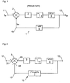
- FIG. 1 shows a general block diagram of a phase locked loop (PLL) 1, as is known from the prior art.
- the PLL 1 has a PLL input 11 and a PLL output 12.
- the PLL 1 includes a phase detector section comprising a combiner device 2 and a phase detector 3, a low-pass filter 4, a voltage controlled oscillator (VCO) 5 and a frequency divider 6.
- the PLL 1 forms a feedback system, with a feedback loop 13.
- an input signal of an input frequency ( f in ) may be presented.
- the PLL provides a VCO signal of output frequency ( f out ) at the PLL output 12.
- the signal with divided frequency f div is combined with the input signal of input frequency by combiner device 2, in this example by determining the difference between the input signal of input frequency and the signal of divided or reference frequency.
- the resulting output signal of the combiner device 2 is transmitted to phase detector 3.
- the phase detector 3 outputs a difference signal which is based on the difference in phase between the signal of divided frequency f div and the signal of input frequency f in .
- the difference signal is low-pass filtered by filter 4 and used as the VCO input signal which controls the oscillation of the VCO 5.
- the filter section 3 and the frequency divider 6 may be omitted.
- most PLLs comprise a (loop)filter and a frequency divider.
- a current controlled oscillator may be used.
- Fig. 2 shows an example of a PLL 10 according to the invention.
- the PLL 10 has a PLL input 11, a PLL output 12, an combiner device 2, a phase detector 3, a low-pass filter 4 and a voltage controlled oscillator (VCO) 5.
- the PLL 10 also comprises a feedback loop 13. A combined zero and frequency divider device 7 is present in the feedback loop.
- the zero and frequency divider device 7 has a transfer function G(s) with at least one zero.
- H closed (s) H ( s ) 1 + G ( s ) H ( s )
- K D represents the transfer function of the phase detector 3
- H f (s) represents the transfer function of the filter section 4
- K o /s represents the transfer function of the VCO 5.
- the zero device 7 is part of the feedback loop 13, i.e. the zero is integrated in the divider 5.
- the zero in the transfer function of the device 7 is not present as a zero in the closed loop transfer of the PLL.
- Such a zero is often called a phantom zero.
- the zero provides a stable system, but does not decrease the out-of band attenuation.
- the closed-loop bandwidth can be increased for a given rejection at a certain out-of-band spot-frequency compared to the system without the phantom-zero.
- the settling-time after applying a frequency-step is improved, without affecting the out-of-band rejection performance for a certain out-of-band spot-frequency (and higher frequencies).
- the attenuation at an out-of-band frequency ⁇ equal to 5/ ⁇ z is specified due to phase-noise requirements. If the original system (i.e. the system without the zero in the feedback loop) was a third order system with three equal closed-loop poles, the time constant of the system with the zero in the feedback loop can be made 2.5 times smaller to achieve this goal.
- the settling-time for a frequency-step is thus improved by a factor of approximately 2.5 compared to the prior art PLL.
- the improvement-factor will be even larger for out-of-band frequencies higher than 5/ ⁇ z , because of the increased out-of band attenuation.
- the order of the loop may be decreased by one and simultaneously the time-constant may be altered compared to a prior art PLL, while maintaining the same out-of-band rejection performance as compared to the original synthesiser.
- This gives an improvement in the settling-time by a factor of 2.2 when the standard third order system is replaced by a second order system with a zero in the feedback loop. (In which case it is found from simulations that the time constant of a PLL according to the invention may be made 0.58 times smaller compared to that of a prior art PLL).
- the avoidance of a zero in the closed-loop transfer and choosing real closed-loop poles reduces the overshoot in the step-response of the output-frequency.
- the VCO control-signal will have a smaller overshoot when a frequency-step is applied. This allows an increase in the allowable voltage swing of the VCO control-voltage for the same supply voltage. Alternatively, the required supply-voltage for a given swing may be decreased. Hence power consumption is reduced, since for a given swing a lower supply voltage may be used.
- the peaking in the closed-loop phase-transfer is reduced compared to a PLL with a zero in the closed-loop transfer. This implies that no phase-noise amplification will take place at the band-edge.
- the bandwidth may be changed easily during switching by changing the frequency placement of the phantom-zero, optionally in combination with the phase-detector constant. This may for example be performed using a variable time-constant in the zero and/or in the phase-detector, for example using a variable resistor.
- phase-frequency detector due to the presence of the zero in the feedback loop, use of a phase-frequency detector is no longer required to obtain fast locking when large initial frequency-errors exist.
- a simple phase-detector may be used instead, whereby the complexity of the detector is reduced.
- the zero is implemented in a device which also performs the function of the frequency divider.
- the zero may also be implemented in a different way in the feedback loop.
- the PLL of fig. 3 has a feedback loop 13 with a frequency divider 6 and a separate zero device 71.
- the zero device 71 is connected with a zero input 711 to a divider output 62.
- the zero output 712 of the zero device is connected to a reference input 22 of the combiner device 2.
- the PLL in fig. 4 has a feedback loop 13 with two paths 131,132.
- a first path 132 comprises a first frequency divider 72 with a transfer function equal ⁇ z s/N. It should be noted that in a strict sense the divider 72 is an instantaneous phase differentiator, however from this point on, it is referred to as a frequency divider.
- a second path 131 comprises a second frequency divider device 6 with a transfer function of 1/N. The second divider 6 may thus be a conventional divider.
- the frequency dividers are both connected with their output 62 resp. 722 to an input 201,202 of a second combiner device 200.
- the second combiner device 200 is an adder device which adds the signals presented at the combiner inputs 201,202.
- the inputs 61 resp. 721 of the frequency divider devices 6,72 are connected to the output of the VCO 5.
- a second combiner output 203 of the second combiner device 200 is connected to the second input 22 of the combiner device 2.
- the combined transfer function of the feedback loop 13,131,132 is the combined transfer of the frequency divider devices 6,72 and thus equal to (1+ ⁇ z s)/N.
- An advantage of the example of fig. 4, is that it can be used in existing PLL's by inserting the zero in parallel with the already present feedback path .
- This already present feedback path usually contains the frequency divider of the PLL.
- a first feedback loop 131 comprises a frequency divider 6 with a transfer function of 1/N.
- the frequency divider 6 may for example be a conventional frequency divider.
- a second feedback loop 132 comprises a combined phase detector and zero device 73 with a transfer function K D ⁇ z s/N, K D representing a phase detector transfer function.
- the output 32 of the phase detector and the output 732 of the zero device 73 are connected to the inputs 201 and 202 of a second combiner device 210.
- An output of the second combine An output 203 of the second combiner device 200 is connected to the input 41 of the filter section 4.
- the time-constant of the zero device 73 is set to be substantially equal to K D ⁇ z /N, however this is not essential.
- An advantage of the example of a PLL according to the invention of fig. 5 is that it can be very easy implemented in existing PLL's by inserting the zero between the output of the VCO and the output of the phase-detector.
- the frequency divider in the feedback loop may be implemented as a fractional divider or a DeltaSigma-driven frequency divider.
- the output-signal of such a divider may be modelled as the sum of a signal with the wanted phase and a signal with an unwanted noisy phase.
- a zero device 72 is placed between the output of the VCO and the input of the phase-detector.
- a delta-sigma modulator 8 is connected to a control input 63 of a frequency divider 62.
- the zero device 7 is connected with an input 721 to the PLL output 12.
- the output 722 of the zero device 7 is connected to a first input 201 of a second combiner device 200.
- a second input 202 of the combiner device 200 is connected to the output 62 of frequency divider 6.
- the combiner device 200 adds the signals presented at the inputs 201,202.
- the zero is realised in front of the divider output-signal and not behind this signal.
- the zero may likewise be placed between the original output-signal of the divider and the input of the phase-detector.
- the jitter in the divider may be compensated by an equal amount of jitter in the zero.
- This compensation-signal can be derived from the circuitry that is controlling the fractional divider. In fig. 7 an example of a PLL with such compensation is shown.
- Fig. 7 shows a PLL with a delta-sigma driven frequency divider 6.
- a control input 63 of the frequency divider 6 is connected to a delta-sigma modulator 8.
- the delta-sigma modulator 8 is also connected to a second combiner device 210 and a first input 741 of a zero device 74.
- the zero device 74 is connected with a second input 742 to the output of the frequency divider 6.
- the output of the zero device 74 is connected to a second input 22 of a first combiner 2.
- the second combiner device 210 is connected with a first input 201 to the output of the phase detector 3.
- the output 203 of the second combiner device 210 is connected to the filter section 4.
- the zero device 71 is implemented between the frequency divider 61 and the VCO 5.
- An input 711 of the zero device is connected to the output of the VCO and an output 712 of the zero device is connected to the input 62 of the frequency divider 6.
- the zero device 7 has a transfer function equal to 1+ ⁇ s s.
- the zero device is implemented as a single device with said transfer function.
- the required transfer function may be obtained by a device 75 with a transfer equal to ⁇ s s connected with the input 752 and output 751 to the inputs of a combiner device 22.
- a PLL according to the invention may be implemented with analog devices and/or digital devices and/or software.
- the zero in the feedback loop may be implemented either in the analog domain and/or in the digital-domain and/or software.
- the zero may be implemented in any appropriate manner.
- the zero may for instance be implemented as a frequency discriminator.
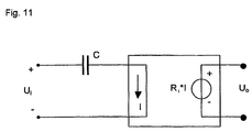
- An example of such a frequency discriminator device 900 is shown in fig. 10.
- the discriminator comprises a delay-device 910, a multiplier-element 920 and a low-pass filter 930.
- the delay device is connected with both the input and the output to the inputs of the multiplier.
- An output of the multiplier is connected to the input of the filter 930.
- the output-signal is proportional to small frequency-deviations relative to ⁇ o .
- the low-pass filter 930 may be combined with a filter already present in the PLL.
- the frequency discriminator of fig. 11 comprises a capacitor connected between the positive and negative contacts of an input u i of the discriminator. Connected to the capacitor is an amplifier device R t I which provides a signal which is proportional to the current between the input contacts. For example,supposing the input signal is equal to A*cos ( ⁇ (t)), the capacitor has a capacitance C and the amplifier an amplification Rt, the output signal of the discriminator of fig. 11 is equal to R t *C*A*sin( ⁇ t)*d( ⁇ (t))/dt,
- the zero may also be implemented in a different way, for example using a different frequency discriminator, such as the all digital frequency discriminator known from Beards at al., "An oversampling Delta-sigma frequency dscriminator", IEEE Transactions on Circuits and Systems-II: Analog and digital signal processing” , vol. 41, no. 1, January 1994, pp. 26-32.
- a different frequency discriminator such as the all digital frequency discriminator known from Beards at al., "An oversampling Delta-sigma frequency dscriminator", IEEE Transactions on Circuits and Systems-II: Analog and digital signal processing” , vol. 41, no. 1, January 1994, pp. 26-32.
- a PLL or synthesiser according to the invention may be used in a (portable-) communication device, in order to generate one or more periodic signals.
- the PLL may for example be required to translate a received radio-signal to a lower frequency or to translate a signal to be transmitted to the desired radio frequency.
- the synthesizer or PLL can be switched as quickly as possible.
- fast frequency hopping systems such as systems operating in accordance with the Bluetooth protocol
- the settling-time of the PLL is a major issue.
- a PLL according to the invention is especially suited for use in such systems.
Landscapes
- Stabilization Of Oscillater, Synchronisation, Frequency Synthesizers (AREA)
Claims (16)
- Phasenregelkreis-Schaltkreis (PLL-Schaltkreis) 1, der mindestens Folgendes aufweist:einen Regelkreis-Eingang (11);einen Phasendetektor-Abschnitt (2, 3) zum Erkennen einer Phasendifferenz zwischen einem Eingangssignal und einem Bezugssignal, wobei der Phasendetektor-Abschnitt (2, 3) einen mit dem Regelkreis-Eingang verbundenen Detektor-Eingang, einen Bezugseingang und einen Detektor-Ausgang zum Ausgeben eines sich auf die Phasendifferenz beziehenden Signals hat;einen gesteuerten Oszillator (4) mit einem Eingang, der mit dem Detektor-Ausgang kommunikativ verbunden ist, und einem Oszillator-Ausgang, der mit einem Regelkreis-Ausgang (12) verbunden ist; undeine Rückkopplungsschaltung (13), die den Oszillator-Ausgang mit dem Bezugseingang verbindet,dadurch gekennzeichnet, dass die Rückkopplungsschaltung ein Bauelement (7; 71 - 74) mit einer Übertragungsfunktion mit mindestens einer Nullstelle hat und der Phasenregelkreis-Schaltkreis (1) eine Regelkreis-Übertragungsfunktion ohne Nullstellen hat
- Phasenregelkreis-Schaltkreis nach Anspruch 1, der weiterhin einen Filter-Abschnitt (4) aufweist, der einen mit dem Detektor-Ausgang verbundenen Filter-Eingang und einen mit dem Oszillator-Eingang verbundenen Filter-Ausgang hat.
- Phasenregelkreis-Schaltkreis nach Anspruch 1 oder 2, dadurch gekennzeichnet, dass die Rückkopplungsschaltung weiterhin mindestens einen Frequenzteiler (6; 7; 72; 73) aufweist.
- Phasenregelkreis-Schaltkreis nach Anspruch 3, dadurch gekennzeichnet, dass der Frequenzteiler mit einem Delta-Sigma-Modulator (8) verbunden ist
- Phasenregelkreis-Schaltkreis nach Anspruch 3 oder 4, dadurch gekennzeichnet, dass der Frequenzteiler (6; 7; 72) eine Übertragungsfunktion mit der Nullstelle hat.
- Phasenregelkreis-Schaltkreis nach einem der Ansprüche 3-5, dadurch gekennzeichnet, dass die Rückkopplungssehaltung einen ersten Frequenzteiler (6) und einen zweiten Frequenzteiler (7; 72; 73) aufweist, wobei der zweite Frequenzteiler eine Übertragungsfunktion mit einer Nullstelle hat.
- Phasenregelkreis-Schaltkreis nach Anspruch 6, dadurch gekennzeichnet, dass der erste Frequenzteiler (6) und der zweite Frequenzteiler (7; 72; 73) parallel geschaltet sind, dass ein Eingang des ersten Frequenzteilers und ein Ausgang des zweiten Frequenzteilers jeweils mit einem Eingang eines zweiten Kombinators (200) verbunden sind und dass ein Ausgang des zweiten Kombinators mit dem Bezugseingang des Phasendetektor-Abschnitts (2, 3) verbunden ist.
- Phasenregelkreis-Schaltkreis nach Anspruch 6, dadurch gekennzeichnet, dass ein Ausgang des zweiten Frequenzteilers (73) mit einem ersten Eingang eines zweiten Kombinators (210) verbunden ist, ein zweiter Eingang des zweiten Kombinators mit dem Ausgang des Phasendetektors verbunden ist, ein Ausgang des zweiten Kombinators kommunikativ mit dem spannungsgesteuerten Oszillator (VCO) verbunden ist und dass der zweite Frequenzteiler einen Phasendetektor-Abschnitt aufweist und eine Übertragungsfunktion mit der Nullstelle hat.
- Phasenregelkreis-Schaltkreis nach einem der Ansprüche 3 - 5, dadurch gekennzeichnet, dass der Frequenzteiler (6) mit einem Bauelement (71; 74; 75), das eine Übertragungsfunktion mit einer Nullstelle hat, in Reihe geschaltet ist.
- Phasenregelkreis-Schaltkreis nach Anspruch 9, dadurch gekennzeichnet, dass das Bauelement (71; 75), das eine Übertragungsfunktion mit einer Nullstelle hat, einen Eingang, der mit dem gesteuerten Oszillator (5) verbunden ist, und einen Ausgang, der mit einem Eingang (61) des Frequenzteilers (6) verbunden ist, hat.
- Phasenregelkreis-Schaltkreis nach Anspruch 9, dadurch gekennzeichnet, dass das Bauelement (71; 75), das eine Übertragungsfunktion mit einer Nullstelle hat, einen Eingang, der mit einem Ausgang des Frequenzteilers (6) verbunden ist, und einen Ausgang, der mit einem Eingang des Phasendetektor-Abschnitts verbunden ist, hat.
- Phasenregelkreis-Schaltkreis nach Anspruch 4 und 11, dadurch gekennzeichnet, dass das Bauelement (74), das eine Übertragungsfunktion mit einer Nullstelle hat, einen ersten Eingang (741), der mit dem Delta-Sigma-Modulator (8) verbunden ist, und einen zweiten Eingang (742), der mit dem Ausgang des Frequenzteilers (6) verbunden ist, hat.
- Phasenregelkreis-Schaltkreis nach Anspruch 10, dadurch gekennzeichnet, dass das Bauelement (71; 75), das eine Übertragungsfunktion mit einer Nullstelle hat, ein Bauelement (75) mit einer Übertragungsfunktion, die gleich τss ist, das einen mit dem Ausgang des Oszillators (4) verbundenen Bauelement-Eingang (751) hat, umfasst, wobei das Bauelement (71; 75), das eine Übertragungsfunktion mit einer Nullstelle hat, weiterhin einen Kombinator (22) aufweist, der Folgendes aufweist:einen ersten Kombinator-Eingang, der mit dem Ausgang des Bauelements (75) mit einer Übertragungsfunktion, die gleich τss ist, verbunden ist;einen zweiten Komparator-Eingang, der mit dem Eingang des Bauelements (75) mit einer Übertragungsfunktion, die gleich τss ist, verbunden ist; undeinen Kombinator-Ausgang, der mit dem Eingang des Frequenzteilers (6) verbunden ist.
- Verfahren zum Erzeugen eines periodischen Signals, das mindestens Folgendes aufweist:Empfangen eines periodischen Signals mit einer ersten Frequenz:dadurch gekennzeichnet, dass zum Ändern des Ausgangssignals eine Rückkopplungsschaltung mit einer Übertragungsfunktion mit mindestens einer Nullstelle verwendet wird und zum Empfangen eines periodischen Signals bis zum Senden des Ausgangssignals eine Regelkreis-Übertragungsfunktion ohne Nullstellen verwendet wird.Vergleichen einer Phase des periodischen Signals mit einer Phase eines Bezugssignals;Erzeugen eines Differenzsignals, das sich auf die Phasendifferenz zwischen dem periodischen Signal und dem Bezugssignal bezieht;Filtem des Differenzsignals;Erzeugen eines Ausgangssignals mit einer Frequenz, die einer Amplitude des Differenzsignals entspricht;Weitersenden des Ausgangssignals undErzeugen des Bezugssignals durch Ändern des Ausgangssignals in einer Weise, dass die Frequenz des Ausgangssignals verringert wird,
- Elektronisches Gerät mit einem Phasenregelkreis-Schaltkreis nach einem der Ansprüche 1 - 13.
- Funkgerät zumindest mit einem Phasenregelkreis-Schaltkreis nach einem der Ansprüche 1 - 13.
Priority Applications (1)
| Application Number | Priority Date | Filing Date | Title |
|---|---|---|---|
| AT02743985T ATE329408T1 (de) | 2002-07-03 | 2002-07-03 | Phasenregelkreisschaltung, elektronische vorrichtung mit einer phasenregelkreisschaltung und verfahren zur erzeugung eines periodischen signals |
Applications Claiming Priority (1)
| Application Number | Priority Date | Filing Date | Title |
|---|---|---|---|
| PCT/NL2002/000436 WO2004006437A1 (en) | 2002-07-03 | 2002-07-03 | Phase locked loop circuit, electronic device including a phase locked loop circuit and method for generating a periodic signal |
Publications (2)
| Publication Number | Publication Date |
|---|---|
| EP1518324A1 EP1518324A1 (de) | 2005-03-30 |
| EP1518324B1 true EP1518324B1 (de) | 2006-06-07 |
Family
ID=30113363
Family Applications (1)
| Application Number | Title | Priority Date | Filing Date |
|---|---|---|---|
| EP02743985A Expired - Lifetime EP1518324B1 (de) | 2002-07-03 | 2002-07-03 | Phasenregelkreisschaltung, elektronische vorrichtung mit einer phasenregelkreisschaltung und verfahren zur erzeugung eines periodischen signals |
Country Status (7)
| Country | Link |
|---|---|
| US (1) | US7391840B2 (de) |
| EP (1) | EP1518324B1 (de) |
| JP (1) | JP4323425B2 (de) |
| CN (1) | CN100477528C (de) |
| AU (1) | AU2002345446A1 (de) |
| DE (1) | DE60212203D1 (de) |
| WO (1) | WO2004006437A1 (de) |
Families Citing this family (8)
| Publication number | Priority date | Publication date | Assignee | Title |
|---|---|---|---|---|
| US8392857B2 (en) * | 2008-12-04 | 2013-03-05 | Synopsys, Inc. | Automated circuit design process for generation of stability constraints for generically defined electronic system with feedback |
| US8316330B2 (en) * | 2009-12-09 | 2012-11-20 | Anupam Bakshi | System and method for circuit design automation |
| US8736328B2 (en) * | 2011-12-22 | 2014-05-27 | Intel Corporation | Low power, jitter and latency clocking with common reference clock signals for on-package input/output interfaces |
| US9660797B2 (en) | 2013-03-21 | 2017-05-23 | Telefonaktiebolaget Lm Ericsson (Publ) | Method and apparatus for implementing clock holdover |
| US9258000B1 (en) * | 2014-09-23 | 2016-02-09 | Infineon Technologies Ag | Combined lock/out-of-lock detector for phase locked loops |
| CN110380725B (zh) * | 2019-05-30 | 2023-06-20 | 芯创智创新设计服务中心(宁波)有限公司 | 一种鉴频鉴相模块的增益控制系统及方法 |
| CN120090270B (zh) * | 2025-01-02 | 2026-01-23 | 北京交通大学 | 虚拟同步发电机控制方法及系统 |
| CN119966527A (zh) * | 2025-01-27 | 2025-05-09 | 中国科学院半导体研究所 | 一种高性能集成信号源 |
Family Cites Families (9)
| Publication number | Priority date | Publication date | Assignee | Title |
|---|---|---|---|---|
| CA2123477A1 (en) * | 1994-05-12 | 1995-11-13 | Thomas Atkin Denning Riley | Delta-sigma fractional-n frequency synthesizer and frequency discriminator suitable for use therein |
| US5550515A (en) * | 1995-01-27 | 1996-08-27 | Opti, Inc. | Multiphase clock synthesizer having a plurality of phase shifted inputs to a plurality of phase comparators in a phase locked loop |
| US5504459A (en) * | 1995-03-20 | 1996-04-02 | International Business Machines Corporation | Filter network for phase-locked loop circuit |
| GB2320629B (en) * | 1996-12-23 | 2001-04-25 | Nokia Mobile Phones Ltd | A radio transmitter and phase locked loop therefor |
| US6008703A (en) * | 1997-01-31 | 1999-12-28 | Massachusetts Institute Of Technology | Digital compensation for wideband modulation of a phase locked loop frequency synthesizer |
| JP3992786B2 (ja) * | 1997-06-06 | 2007-10-17 | 富士通株式会社 | 論理検証方法、論理検証装置及び記録媒体 |
| US6011815A (en) * | 1997-09-16 | 2000-01-04 | Telefonaktiebolaget Lm Ericsson | Compensated ΔΣ controlled phase locked loop modulator |
| US6249189B1 (en) * | 1998-08-05 | 2001-06-19 | National Science Council Of Republic Of China | Frequency synthesizer accomplished by using multiphase reference signal source |
| US6570452B2 (en) * | 2001-09-26 | 2003-05-27 | Ashvattha Semiconductor, Inc. | Fractional-N type frequency synthesizer |
-
2002
- 2002-07-03 EP EP02743985A patent/EP1518324B1/de not_active Expired - Lifetime
- 2002-07-03 US US10/517,181 patent/US7391840B2/en not_active Expired - Lifetime
- 2002-07-03 CN CNB028292685A patent/CN100477528C/zh not_active Expired - Fee Related
- 2002-07-03 AU AU2002345446A patent/AU2002345446A1/en not_active Abandoned
- 2002-07-03 DE DE60212203T patent/DE60212203D1/de not_active Expired - Lifetime
- 2002-07-03 WO PCT/NL2002/000436 patent/WO2004006437A1/en not_active Ceased
- 2002-07-03 JP JP2004519355A patent/JP4323425B2/ja not_active Expired - Fee Related
Also Published As
| Publication number | Publication date |
|---|---|
| US20060165206A1 (en) | 2006-07-27 |
| CN1639980A (zh) | 2005-07-13 |
| JP4323425B2 (ja) | 2009-09-02 |
| US7391840B2 (en) | 2008-06-24 |
| WO2004006437A1 (en) | 2004-01-15 |
| JP2005536917A (ja) | 2005-12-02 |
| AU2002345446A1 (en) | 2004-01-23 |
| CN100477528C (zh) | 2009-04-08 |
| EP1518324A1 (de) | 2005-03-30 |
| DE60212203D1 (de) | 2006-07-20 |
Similar Documents
| Publication | Publication Date | Title |
|---|---|---|
| US8531219B1 (en) | Phase locked loop with digital compensation for analog integration | |
| US7177611B2 (en) | Hybrid control of phase locked loops | |
| US6594330B1 (en) | Phase-locked loop with digitally controlled, frequency-multiplying oscillator | |
| EP2312756B1 (de) | Doppelreferenzoszillator-Phasenregelschleife | |
| JP4629310B2 (ja) | 位相同期回路 | |
| US6900675B2 (en) | All digital PLL trimming circuit | |
| EP1371167B1 (de) | Fraktional-n-frequenzsynthesizer mit fraktional-kompensationsverfahren | |
| JP2000252819A (ja) | Pll回路 | |
| US7084709B1 (en) | Hybrid analog/digital phase lock loop frequency synthesizer | |
| EP1518324B1 (de) | Phasenregelkreisschaltung, elektronische vorrichtung mit einer phasenregelkreisschaltung und verfahren zur erzeugung eines periodischen signals | |
| Mirabbasi et al. | Design of loop filter in phase-locked loops | |
| EP1897221B1 (de) | Phasenregelkreissysteme mit adaptiven tiefpassfiltern in feedbackschleifen mit geschalteter bandbreite | |
| KR102392119B1 (ko) | 위상 회전자를 이용한 분수 서브 샘플링 위상 고정 루프 | |
| KR100910086B1 (ko) | 위상 고정 루프 회로, 위상 고정 루프 회로를 포함하는전자 장치 및 주기 신호를 발생시키는 방법 | |
| KR100830898B1 (ko) | 전압 제어 발진기의 출력 클럭으로 동작하는 스위치드커패시터 네트워크를 이용한 위상 고정 루프 및 제어방법 | |
| EP1107458B1 (de) | System zum Begrenzen der Zwischenfrequenzänderung in Phasenregelkreisen | |
| JP3567779B2 (ja) | シンセサイザ及び基準信号生成回路 | |
| Konwar et al. | Some aspects of modelling and simulation of a high frequency and fast settling time proportional-integral-derivative controlled phase-locked loop | |
| JPH10126263A (ja) | 周波数シンセサイザ装置 | |
| Heuermann | Phase-Locked Loops and Synthesis Generators | |
| WO2020148517A1 (en) | Phase-locked loop circuitry | |
| Chau et al. | All-digital phase-locked loop with an adaptive bandwidth design procedure | |
| Holtzman et al. | A DIGITAL INTEGRATOR FOR AN S-BAND HIGH-SPEED FREQUENCY-HOPPING PHASE-LOCKED LOOP | |
| JPH06326603A (ja) | Pll周波数シンセサイザ回路 | |
| JP2005303996A (ja) | 周波数変調装置 |
Legal Events
| Date | Code | Title | Description |
|---|---|---|---|
| PUAI | Public reference made under article 153(3) epc to a published international application that has entered the european phase |
Free format text: ORIGINAL CODE: 0009012 |
|
| 17P | Request for examination filed |
Effective date: 20041207 |
|
| AK | Designated contracting states |
Kind code of ref document: A1 Designated state(s): AT BE BG CH CY CZ DE DK EE ES FI FR GB GR IE IT LI LU MC NL PT SE SK TR |
|
| AX | Request for extension of the european patent |
Extension state: AL LT LV MK RO SI |
|
| GRAP | Despatch of communication of intention to grant a patent |
Free format text: ORIGINAL CODE: EPIDOSNIGR1 |
|
| DAX | Request for extension of the european patent (deleted) | ||
| GRAC | Information related to communication of intention to grant a patent modified |
Free format text: ORIGINAL CODE: EPIDOSCIGR1 |
|
| GRAS | Grant fee paid |
Free format text: ORIGINAL CODE: EPIDOSNIGR3 |
|
| GRAA | (expected) grant |
Free format text: ORIGINAL CODE: 0009210 |
|
| RIN1 | Information on inventor provided before grant (corrected) |
Inventor name: EIKENBROEK, JOHANNES, WILHELMUS, THEODORUS |
|
| AK | Designated contracting states |
Kind code of ref document: B1 Designated state(s): AT BE BG CH CY CZ DE DK EE ES FI FR GB GR IE IT LI LU MC NL PT SE SK TR |
|
| PG25 | Lapsed in a contracting state [announced via postgrant information from national office to epo] |
Ref country code: IT Free format text: LAPSE BECAUSE OF FAILURE TO SUBMIT A TRANSLATION OF THE DESCRIPTION OR TO PAY THE FEE WITHIN THE PRESCRIBED TIME-LIMIT;WARNING: LAPSES OF ITALIAN PATENTS WITH EFFECTIVE DATE BEFORE 2007 MAY HAVE OCCURRED AT ANY TIME BEFORE 2007. THE CORRECT EFFECTIVE DATE MAY BE DIFFERENT FROM THE ONE RECORDED. Effective date: 20060607 Ref country code: CZ Free format text: LAPSE BECAUSE OF FAILURE TO SUBMIT A TRANSLATION OF THE DESCRIPTION OR TO PAY THE FEE WITHIN THE PRESCRIBED TIME-LIMIT Effective date: 20060607 Ref country code: FI Free format text: LAPSE BECAUSE OF FAILURE TO SUBMIT A TRANSLATION OF THE DESCRIPTION OR TO PAY THE FEE WITHIN THE PRESCRIBED TIME-LIMIT Effective date: 20060607 Ref country code: NL Free format text: LAPSE BECAUSE OF FAILURE TO SUBMIT A TRANSLATION OF THE DESCRIPTION OR TO PAY THE FEE WITHIN THE PRESCRIBED TIME-LIMIT Effective date: 20060607 Ref country code: AT Free format text: LAPSE BECAUSE OF FAILURE TO SUBMIT A TRANSLATION OF THE DESCRIPTION OR TO PAY THE FEE WITHIN THE PRESCRIBED TIME-LIMIT Effective date: 20060607 Ref country code: BE Free format text: LAPSE BECAUSE OF FAILURE TO SUBMIT A TRANSLATION OF THE DESCRIPTION OR TO PAY THE FEE WITHIN THE PRESCRIBED TIME-LIMIT Effective date: 20060607 Ref country code: CH Free format text: LAPSE BECAUSE OF FAILURE TO SUBMIT A TRANSLATION OF THE DESCRIPTION OR TO PAY THE FEE WITHIN THE PRESCRIBED TIME-LIMIT Effective date: 20060607 Ref country code: LI Free format text: LAPSE BECAUSE OF FAILURE TO SUBMIT A TRANSLATION OF THE DESCRIPTION OR TO PAY THE FEE WITHIN THE PRESCRIBED TIME-LIMIT Effective date: 20060607 Ref country code: SK Free format text: LAPSE BECAUSE OF FAILURE TO SUBMIT A TRANSLATION OF THE DESCRIPTION OR TO PAY THE FEE WITHIN THE PRESCRIBED TIME-LIMIT Effective date: 20060607 |
|
| REG | Reference to a national code |
Ref country code: GB Ref legal event code: FG4D |
|
| REG | Reference to a national code |
Ref country code: CH Ref legal event code: EP |
|
| PG25 | Lapsed in a contracting state [announced via postgrant information from national office to epo] |
Ref country code: IE Free format text: LAPSE BECAUSE OF NON-PAYMENT OF DUE FEES Effective date: 20060703 |
|
| REG | Reference to a national code |
Ref country code: IE Ref legal event code: FG4D |
|
| REF | Corresponds to: |
Ref document number: 60212203 Country of ref document: DE Date of ref document: 20060720 Kind code of ref document: P |
|
| PG25 | Lapsed in a contracting state [announced via postgrant information from national office to epo] |
Ref country code: MC Free format text: LAPSE BECAUSE OF NON-PAYMENT OF DUE FEES Effective date: 20060731 |
|
| PG25 | Lapsed in a contracting state [announced via postgrant information from national office to epo] |
Ref country code: SE Free format text: LAPSE BECAUSE OF FAILURE TO SUBMIT A TRANSLATION OF THE DESCRIPTION OR TO PAY THE FEE WITHIN THE PRESCRIBED TIME-LIMIT Effective date: 20060907 Ref country code: DK Free format text: LAPSE BECAUSE OF FAILURE TO SUBMIT A TRANSLATION OF THE DESCRIPTION OR TO PAY THE FEE WITHIN THE PRESCRIBED TIME-LIMIT Effective date: 20060907 |
|
| PG25 | Lapsed in a contracting state [announced via postgrant information from national office to epo] |
Ref country code: DE Free format text: LAPSE BECAUSE OF FAILURE TO SUBMIT A TRANSLATION OF THE DESCRIPTION OR TO PAY THE FEE WITHIN THE PRESCRIBED TIME-LIMIT Effective date: 20060908 |
|
| PG25 | Lapsed in a contracting state [announced via postgrant information from national office to epo] |
Ref country code: ES Free format text: LAPSE BECAUSE OF FAILURE TO SUBMIT A TRANSLATION OF THE DESCRIPTION OR TO PAY THE FEE WITHIN THE PRESCRIBED TIME-LIMIT Effective date: 20060918 |
|
| PG25 | Lapsed in a contracting state [announced via postgrant information from national office to epo] |
Ref country code: PT Free format text: LAPSE BECAUSE OF FAILURE TO SUBMIT A TRANSLATION OF THE DESCRIPTION OR TO PAY THE FEE WITHIN THE PRESCRIBED TIME-LIMIT Effective date: 20061107 |
|
| NLV1 | Nl: lapsed or annulled due to failure to fulfill the requirements of art. 29p and 29m of the patents act | ||
| REG | Reference to a national code |
Ref country code: CH Ref legal event code: PL |
|
| ET | Fr: translation filed | ||
| PLBE | No opposition filed within time limit |
Free format text: ORIGINAL CODE: 0009261 |
|
| STAA | Information on the status of an ep patent application or granted ep patent |
Free format text: STATUS: NO OPPOSITION FILED WITHIN TIME LIMIT |
|
| 26N | No opposition filed |
Effective date: 20070308 |
|
| PG25 | Lapsed in a contracting state [announced via postgrant information from national office to epo] |
Ref country code: GR Free format text: LAPSE BECAUSE OF FAILURE TO SUBMIT A TRANSLATION OF THE DESCRIPTION OR TO PAY THE FEE WITHIN THE PRESCRIBED TIME-LIMIT Effective date: 20060908 |
|
| PG25 | Lapsed in a contracting state [announced via postgrant information from national office to epo] |
Ref country code: BG Free format text: LAPSE BECAUSE OF FAILURE TO SUBMIT A TRANSLATION OF THE DESCRIPTION OR TO PAY THE FEE WITHIN THE PRESCRIBED TIME-LIMIT Effective date: 20060907 Ref country code: EE Free format text: LAPSE BECAUSE OF FAILURE TO SUBMIT A TRANSLATION OF THE DESCRIPTION OR TO PAY THE FEE WITHIN THE PRESCRIBED TIME-LIMIT Effective date: 20060607 |
|
| PG25 | Lapsed in a contracting state [announced via postgrant information from national office to epo] |
Ref country code: TR Free format text: LAPSE BECAUSE OF FAILURE TO SUBMIT A TRANSLATION OF THE DESCRIPTION OR TO PAY THE FEE WITHIN THE PRESCRIBED TIME-LIMIT Effective date: 20060607 Ref country code: LU Free format text: LAPSE BECAUSE OF NON-PAYMENT OF DUE FEES Effective date: 20060703 |
|
| PG25 | Lapsed in a contracting state [announced via postgrant information from national office to epo] |
Ref country code: CY Free format text: LAPSE BECAUSE OF FAILURE TO SUBMIT A TRANSLATION OF THE DESCRIPTION OR TO PAY THE FEE WITHIN THE PRESCRIBED TIME-LIMIT Effective date: 20060607 |
|
| REG | Reference to a national code |
Ref country code: FR Ref legal event code: PLFP Year of fee payment: 14 |
|
| PGFP | Annual fee paid to national office [announced via postgrant information from national office to epo] |
Ref country code: GB Payment date: 20150727 Year of fee payment: 14 |
|
| PGFP | Annual fee paid to national office [announced via postgrant information from national office to epo] |
Ref country code: FR Payment date: 20150717 Year of fee payment: 14 |
|
| GBPC | Gb: european patent ceased through non-payment of renewal fee |
Effective date: 20160703 |
|
| PG25 | Lapsed in a contracting state [announced via postgrant information from national office to epo] |
Ref country code: FR Free format text: LAPSE BECAUSE OF NON-PAYMENT OF DUE FEES Effective date: 20160801 |
|
| REG | Reference to a national code |
Ref country code: FR Ref legal event code: ST Effective date: 20170331 |
|
| PG25 | Lapsed in a contracting state [announced via postgrant information from national office to epo] |
Ref country code: GB Free format text: LAPSE BECAUSE OF NON-PAYMENT OF DUE FEES Effective date: 20160703 |