EP1519398A2 - Panneau d'affichage à plasma - Google Patents
Panneau d'affichage à plasma Download PDFInfo
- Publication number
- EP1519398A2 EP1519398A2 EP04022518A EP04022518A EP1519398A2 EP 1519398 A2 EP1519398 A2 EP 1519398A2 EP 04022518 A EP04022518 A EP 04022518A EP 04022518 A EP04022518 A EP 04022518A EP 1519398 A2 EP1519398 A2 EP 1519398A2
- Authority
- EP
- European Patent Office
- Prior art keywords
- cell
- display panel
- plasma display
- horizontal
- cells
- Prior art date
- Legal status (The legal status is an assumption and is not a legal conclusion. Google has not performed a legal analysis and makes no representation as to the accuracy of the status listed.)
- Granted
Links
Images




Classifications
-
- H—ELECTRICITY
- H01—ELECTRIC ELEMENTS
- H01J—ELECTRIC DISCHARGE TUBES OR DISCHARGE LAMPS
- H01J11/00—Gas-filled discharge tubes with alternating current induction of the discharge, e.g. alternating current plasma display panels [AC-PDP]; Gas-filled discharge tubes without any main electrode inside the vessel; Gas-filled discharge tubes with at least one main electrode outside the vessel
- H01J11/20—Constructional details
- H01J11/34—Vessels, containers or parts thereof, e.g. substrates
- H01J11/36—Spacers, barriers, ribs, partitions or the like
-
- H—ELECTRICITY
- H01—ELECTRIC ELEMENTS
- H01J—ELECTRIC DISCHARGE TUBES OR DISCHARGE LAMPS
- H01J11/00—Gas-filled discharge tubes with alternating current induction of the discharge, e.g. alternating current plasma display panels [AC-PDP]; Gas-filled discharge tubes without any main electrode inside the vessel; Gas-filled discharge tubes with at least one main electrode outside the vessel
- H01J11/20—Constructional details
-
- H—ELECTRICITY
- H01—ELECTRIC ELEMENTS
- H01J—ELECTRIC DISCHARGE TUBES OR DISCHARGE LAMPS
- H01J11/00—Gas-filled discharge tubes with alternating current induction of the discharge, e.g. alternating current plasma display panels [AC-PDP]; Gas-filled discharge tubes without any main electrode inside the vessel; Gas-filled discharge tubes with at least one main electrode outside the vessel
- H01J11/10—AC-PDPs with at least one main electrode being out of contact with the plasma
- H01J11/12—AC-PDPs with at least one main electrode being out of contact with the plasma with main electrodes provided on both sides of the discharge space
-
- H—ELECTRICITY
- H01—ELECTRIC ELEMENTS
- H01J—ELECTRIC DISCHARGE TUBES OR DISCHARGE LAMPS
- H01J11/00—Gas-filled discharge tubes with alternating current induction of the discharge, e.g. alternating current plasma display panels [AC-PDP]; Gas-filled discharge tubes without any main electrode inside the vessel; Gas-filled discharge tubes with at least one main electrode outside the vessel
- H01J11/20—Constructional details
- H01J11/34—Vessels, containers or parts thereof, e.g. substrates
- H01J11/44—Optical arrangements or shielding arrangements, e.g. filters, black matrices, light reflecting means or electromagnetic shielding means
-
- H—ELECTRICITY
- H01—ELECTRIC ELEMENTS
- H01J—ELECTRIC DISCHARGE TUBES OR DISCHARGE LAMPS
- H01J2211/00—Plasma display panels with alternate current induction of the discharge, e.g. AC-PDPs
- H01J2211/20—Constructional details
- H01J2211/34—Vessels, containers or parts thereof, e.g. substrates
- H01J2211/36—Spacers, barriers, ribs, partitions or the like
- H01J2211/361—Spacers, barriers, ribs, partitions or the like characterized by the shape
- H01J2211/365—Pattern of the spacers
-
- H—ELECTRICITY
- H01—ELECTRIC ELEMENTS
- H01J—ELECTRIC DISCHARGE TUBES OR DISCHARGE LAMPS
- H01J2211/00—Plasma display panels with alternate current induction of the discharge, e.g. AC-PDPs
- H01J2211/20—Constructional details
- H01J2211/34—Vessels, containers or parts thereof, e.g. substrates
- H01J2211/44—Optical arrangements or shielding arrangements, e.g. filters or lenses
- H01J2211/444—Means for improving contrast or colour purity, e.g. black matrix or light shielding means
Definitions
- the present invention relates to a plasma display panel, and more particularly, to the cell structure of a plasma display panel.
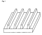
- FIG. 1 illustrates a stripe type barrier rib structure of a conventional plasma display panel.
- FIG. 2 illustrates a well type barrier rib structure of a conventional plasma display panel.
- the stripe type structure shown in FIG. 1 has a good discharge characteristic, but has a disadvantage that the phosphor covering area is small.
- the well type structure shown in FIG. 2 has high brightness since the covering area of phosphors is wide, but has a problem that the discharge characteristic is bad.
- FIG. 3 illustrates a delta type barrier rib structure of a conventional plasma display panel.
- the covering area of phosphors is increased and brightness is improved due to increased reflectivity of barrier walls.
- Each color is connected to a narrow channel whereby discharge or injection of a gas is smooth. Further, as a discharge start voltage in the narrow channel is higher than that of a wide channel, there is an advantage in that crosstalk in the barrier rib direction can be prevented. Moreover, brightness and efficiency can be improved even without additional process because the method for fabricating and operating the barrier ribs is the same as a prior art.
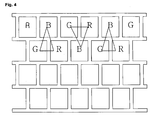
- FIG. 4 illustrates a square type barrier rib structure of a conventional plasma display panel.
- the barrier rib structure shown in FIG. 4 has the same structure as the barrier rib structure of FIG. 3 except that the cell shape is square.
- red, green and blue cells form a triangle similar to the delta type barrier rib structure and thus constitute one cell.
- the square barrier rib structure of FIG. 4 is the same as the delta type barrier rib structure of FIG.3 in that brightness and efficiency are increased due to increase in the aperture ratio and the phosphor covering area.
- the cells are extended sideward lengthily. Therefore, upon implementation of a still image, the still image is not implemented smoothly diagonally. Thus, there is a problem in that the picture quality is degraded.
- an object of the present invention is to solve at least the problems and disadvantages of the background art.
- An object of the present invention is to provide a plasma display panel in which brightness and efficiency are improved and the contrast ratio is improved compared to an existing delta structure.
- a plasma display panel in which square cells constitute a delta type barrier rib structure, wherein a red cell and a green cell are alternately formed in a first horizontal cell line of the cells, a blue cell is located at the lower center between the red cell and the green cell in a second horizontal cell line of the cells, the blue cell is alternately formed together with a blank cell, and the first horizontal cell line and the second horizontal cell line are alternately formed in the vertical direction.
- a plasma display panel in which square cells constitute a delta type barrier rib structure, wherein a red cell and a green cell are alternately formed in a first horizontal cell line of the cells, a blue cell is located at the lower center between the red cell and the green cell in a second horizontal cell line of the cells, the blue cell is alternately formed together with a black cell, and the first horizontal cell line and the second horizontal cell line are alternately formed in the vertical direction.
- FIG. 1 illustrates a stripe type barrier rib structure of a conventional plasma display panel.
- FIG. 2 illustrates a well type barrier rib structure of a conventional plasma display panel.
- FIG. 3 illustrates a delta type barrier rib structure of a conventional plasma display panel.
- FIG. 4 illustrates a square type barrier rib structure of a conventional plasma display panel.
- FIG. 5 illustrates a cell structure of a plasma display panel according to a first embodiment of the present invention.
- FIG. 6 shows a structure in which electrodes of a plasma display panel are arranged according to a first embodiment of the present invention.
- FIG. 7 shows another structure in which electrodes of a plasma display panel are arranged according to a first embodiment of the present invention.
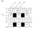
- FIG. 8 shows a cell structure of a plasma display panel according to a second embodiment of the present invention.
- a plasma display panel in which square cells constitute a delta type barrier rib structure, wherein a red cell and a green cell are alternately formed in a first horizontal cell line of the cells, a blue cell is located at the lower center between the red cell and the green cell in a second horizontal cell line of the cells, the blue cell is alternately formed together with a blank cell, and the first horizontal cell line and the second horizontal cell line are alternately formed in the vertical direction.
- the red cell, the green cell and the blue cell constitute one picture element in an inverted triangle shape, and the picture element is parallel to the direction vertical to the horizontal direction.
- Transparent electrodes are formed on the cells in the horizontal direction, bus electrodes are formed at the bottom of the transparent electrodes, and data electrodes are formed on the vertical line of the red cell and the green cell, and the blue cell.
- a data electrode is further disposed on the vertical line of the blank cell.
- FIG. 5 illustrates a cell structure of a plasma display panel according to a first embodiment of the present invention.
- FIG. 5 there is shown a state where red cells 501, green cells 502 and blue cells 503 are arranged.
- the cells are arranged continuously in an inverted triangle shape unlike the structure of FIG. 4 in which the cells are arranged in the regular triangle shape and the inverted triangle shape alternately. That is, in a first horizontal cell line, the red cell 501 and the green cell 502 are alternately formed. In a second horizontal cell line, the blue cell 503 is disposed at the lower center between the red cell 501 and the green cell 502 of the first line, and the blue cell 503 and a cell on which phosphors are not coated (hereinafter, referred to as 'blank cell 504') are alternately formed.
- the first line and the second line are alternately formed in the vertical direction.
- the red cell 501, the green cell 502 and the blue cell 503 constitute one picture element in the form of the inverted triangle.
- the cells are arranged in the regular triangle shape and the inverted triangle shape alternately as shown in FIG. 4, it is difficult to exactly implement a diagonally straight line or a pattern such as a character. If the cells are continuously arranged in the inverted triangle shape, it is possible to implement the same picture quality as the stripe cell.
- one of four pixels in the structure of FIG. 5 has no phosphors and thus remains empty. Accordingly, brightness of the structure shown in FIG. 5 is reduced to about 1/4 of the structure of FIG. 4. However, power consumption can be reduced because electrodes are not disposed in empty pixels. Thus, efficiency is not reduced. Furthermore, brightness of the structure shown in FIG. 5 is lower than that of the structure shown in FIG. 4. However, the aperture ratio and the phosphor coefficient of utilization of phosphors are increased compared to the stripe structure. Therefore, the whole efficiency of the structure shown in FIG. 5 is increased.
- the shape of the pixels is close to the regular square.
- brightness and efficiency are improved since the aperture ratio of the cell is increased.
- FIG. 6 shows a structure in which electrodes of a plasma display panel are arranged according to a first embodiment of the present invention.
- the plasma display panel according to the first embodiment of the present invention includes a first ITO electrode 702a, a second ITO electrode 702b, a first bus electrode 701a, a second bus electrode 701b and a data electrode 703. Further, the first ITO electrode 702a and the second ITO electrode 702b are formed along the horizontal barrier ribs of the cell. A first bus electrode 701a and a second bus electrode 701 b for compensating for high resistance of ITO are formed at the edges of the first ITO electrode 702a and the second ITO electrode 702b.
- the data electrode 703 is formed along the vertical line of the cell.
- the data electrode 703 is formed only on the vertical lines of the red cell 501 and the green cell 502 and on the vertical line of the blue cell 503. That is, the data electrode 703 is removed in the blank cell 504 (this is the same even in the black cell 601) in order to avoid unnecessary power consumption.
- FIG. 7 shows another structure in which electrodes of a plasma display panel are arranged according to a first embodiment of the present invention.
- a first ITO electrode 702a, a second ITO electrode 702b, a first bus electrode 701a, a second bus electrode 701b and a blank cell data electrode 704 are disposed even in the blank cell (or the black cell).
- This is for accomplishing high-speed driving by supplying priming molecule to neighboring cells in such a way that data pulse is always applied to the data electrode 704 of the blank cell (or the black cell) in order to generate address discharging.
- power consumption is the same as the existing delta structure, brightness and efficiency are disadvantageous because brightness is reduced by 25%.
- the amount of reduction of brightness can be compensated through use of high Xe. It is also possible to maintain brightness and efficiency much better than that of the stripe structure.
- a plasma display panel in which square cells constitute a delta type barrier rib structure, wherein a red cell and a green cell are alternately formed in a first horizontal cell line of the cells, a blue cell is located at the lower center between the red cell and the green cell in a second horizontal cell line of the cells, the blue cell is alternately formed together with a black cell, and the first horizontal cell line and the second horizontal cell line are alternately formed in the vertical direction.
- the red cell, the green cell and the blue cell constitute one picture element in an inverted triangle shape, and the picture element is parallel to the direction vertical to the horizontal direction.
- Transparent electrodes are formed on the cells in the horizontal direction, bus electrodes are formed at the edges of the transparent electrodes, and data electrodes are formed on the vertical line of the red cell and the green cell, and the blue cell.
- a data electrode is further disposed on the vertical line of the black cell.
- FIG. 8 shows a cell structure of a plasma display panel according to a second embodiment of the present invention.
- the cell structure of the second embodiment is almost the same as the cell structure of the first embodiment except that it includes a black cell 601 instead of the blank cell. If the blank cell 504 is replaced with the black cell 601 as above, reflectivity of external light can be reduced by 25%. It is thus possible to increase the contrast ratio although a white barrier rib material is used.
- the second embodiment can have the electrode arrangement of FIG. 6 and FIG. 7 like the first embodiment. This leads to the same effect as the first embodiment.
Landscapes
- Physics & Mathematics (AREA)
- Engineering & Computer Science (AREA)
- Plasma & Fusion (AREA)
- Electromagnetism (AREA)
- Gas-Filled Discharge Tubes (AREA)
Applications Claiming Priority (2)
| Application Number | Priority Date | Filing Date | Title |
|---|---|---|---|
| KR2003066612 | 2003-09-25 | ||
| KR10-2003-0066612A KR100527423B1 (ko) | 2003-09-25 | 2003-09-25 | 플라즈마 디스플레이 패널의 구조 |
Publications (3)
| Publication Number | Publication Date |
|---|---|
| EP1519398A2 true EP1519398A2 (fr) | 2005-03-30 |
| EP1519398A3 EP1519398A3 (fr) | 2006-05-17 |
| EP1519398B1 EP1519398B1 (fr) | 2008-03-26 |
Family
ID=34192269
Family Applications (1)
| Application Number | Title | Priority Date | Filing Date |
|---|---|---|---|
| EP04022518A Expired - Lifetime EP1519398B1 (fr) | 2003-09-25 | 2004-09-22 | Panneau d'affichage à plasma |
Country Status (6)
| Country | Link |
|---|---|
| US (1) | US7135818B2 (fr) |
| EP (1) | EP1519398B1 (fr) |
| JP (1) | JP2005100991A (fr) |
| KR (1) | KR100527423B1 (fr) |
| CN (1) | CN1601689A (fr) |
| DE (1) | DE602004012680T2 (fr) |
Cited By (1)
| Publication number | Priority date | Publication date | Assignee | Title |
|---|---|---|---|---|
| EP1746625A2 (fr) | 2005-07-18 | 2007-01-24 | LG Electronics Inc. | Appareil d'affichage à plasma |
Families Citing this family (9)
| Publication number | Priority date | Publication date | Assignee | Title |
|---|---|---|---|---|
| US6822629B2 (en) * | 2000-08-18 | 2004-11-23 | Semiconductor Energy Laboratory Co., Ltd. | Light emitting device |
| KR100548250B1 (ko) * | 2003-08-09 | 2006-02-02 | 엘지전자 주식회사 | 표면 전도형 전계 방출 소자의 매트릭스 구조 |
| US7084567B2 (en) * | 2003-10-20 | 2006-08-01 | .Au Optronics Corporation | Plasma display panel performing high luminance and luminous efficiency |
| KR101125643B1 (ko) * | 2005-07-21 | 2012-03-27 | 삼성에스디아이 주식회사 | 플라즈마 디스플레이 패널 |
| KR100724363B1 (ko) * | 2005-08-10 | 2007-06-04 | 엘지전자 주식회사 | 플라즈마 디스플레이 패널 |
| KR100659094B1 (ko) * | 2005-08-30 | 2006-12-19 | 삼성에스디아이 주식회사 | 플라즈마 디스플레이 패널 |
| KR100649687B1 (ko) * | 2005-10-14 | 2006-11-27 | 엘지전자 주식회사 | 보조 방전 셀을 이용하는 플라즈마 디스플레이 패널 |
| KR100805106B1 (ko) * | 2005-11-29 | 2008-02-21 | 삼성에스디아이 주식회사 | 플라즈마 디스플레이 패널 |
| US20130106891A1 (en) * | 2011-11-01 | 2013-05-02 | Au Optronics Corporation | Method of sub-pixel rendering for a delta-triad structured display |
Family Cites Families (4)
| Publication number | Priority date | Publication date | Assignee | Title |
|---|---|---|---|---|
| JP3918972B2 (ja) * | 1998-06-23 | 2007-05-23 | 株式会社日立プラズマパテントライセンシング | プラズマディスプレイパネル |
| US6787978B2 (en) * | 2000-11-28 | 2004-09-07 | Mitsubishi Denki Kabushiki Kaisha | Plasma display panel and plasma display device |
| JP2003208848A (ja) * | 2002-01-16 | 2003-07-25 | Mitsubishi Electric Corp | 表示装置 |
| KR100548250B1 (ko) * | 2003-08-09 | 2006-02-02 | 엘지전자 주식회사 | 표면 전도형 전계 방출 소자의 매트릭스 구조 |
-
2003
- 2003-09-25 KR KR10-2003-0066612A patent/KR100527423B1/ko not_active Expired - Fee Related
-
2004
- 2004-09-22 EP EP04022518A patent/EP1519398B1/fr not_active Expired - Lifetime
- 2004-09-22 DE DE602004012680T patent/DE602004012680T2/de not_active Expired - Fee Related
- 2004-09-22 US US10/946,353 patent/US7135818B2/en not_active Expired - Fee Related
- 2004-09-24 CN CNA2004100803016A patent/CN1601689A/zh active Pending
- 2004-09-27 JP JP2004279688A patent/JP2005100991A/ja not_active Abandoned
Cited By (2)
| Publication number | Priority date | Publication date | Assignee | Title |
|---|---|---|---|---|
| EP1746625A2 (fr) | 2005-07-18 | 2007-01-24 | LG Electronics Inc. | Appareil d'affichage à plasma |
| EP1746625A3 (fr) * | 2005-07-18 | 2007-05-09 | LG Electronics Inc. | Appareil d'affichage à plasma |
Also Published As
| Publication number | Publication date |
|---|---|
| KR100527423B1 (ko) | 2005-11-09 |
| EP1519398A3 (fr) | 2006-05-17 |
| US20050067960A1 (en) | 2005-03-31 |
| EP1519398B1 (fr) | 2008-03-26 |
| DE602004012680D1 (de) | 2008-05-08 |
| KR20050030676A (ko) | 2005-03-31 |
| JP2005100991A (ja) | 2005-04-14 |
| US7135818B2 (en) | 2006-11-14 |
| CN1601689A (zh) | 2005-03-30 |
| DE602004012680T2 (de) | 2008-07-17 |
Similar Documents
| Publication | Publication Date | Title |
|---|---|---|
| US6348762B1 (en) | Surface discharge type color plasma display panel | |
| US6373195B1 (en) | AC plasma display panel | |
| KR20010022986A (ko) | 가스방전패널 | |
| US7205721B2 (en) | Plasma display panel having discharge space shape with zigzag shaped electrodes | |
| US7135818B2 (en) | Plasma display panel with square cells | |
| US6806645B2 (en) | Plasma display panel | |
| US7352129B2 (en) | Plasma display panel | |
| US7759867B2 (en) | Display panel electrode having a protrusion | |
| US6498594B1 (en) | Plasma display panel and method of driving the same | |
| EP1387386A1 (fr) | Ecran a plasma | |
| US7994717B2 (en) | Plasma display panel and plasma display apparatus using the same | |
| US6392344B1 (en) | Plasma display device | |
| US7459851B2 (en) | Plasma display panel having delta pixel arrangement | |
| US7034459B2 (en) | Front panel structure of plasma display panel | |
| US7755285B2 (en) | Plasma display panel and plasma display apparatus | |
| CN100418178C (zh) | 等离子体显示板 | |
| KR20030095427A (ko) | 플라즈마 디스플레이 패널 | |
| US20050122045A1 (en) | Plasma display panel | |
| EP1632977B1 (fr) | Panneau d'affichage à plasma | |
| US7274146B2 (en) | Electrode structure of a plasma display panel | |
| US20070126360A1 (en) | Plasma display device | |
| US20070046577A1 (en) | Plasma display device | |
| US20090096374A1 (en) | Plasma Display Panel | |
| KR20090004136A (ko) | 플라즈마 디스플레이 패널 | |
| KR20030037728A (ko) | 플라즈마 디스플레이 패널 |
Legal Events
| Date | Code | Title | Description |
|---|---|---|---|
| PUAI | Public reference made under article 153(3) epc to a published international application that has entered the european phase |
Free format text: ORIGINAL CODE: 0009012 |
|
| AK | Designated contracting states |
Kind code of ref document: A2 Designated state(s): AT BE BG CH CY CZ DE DK EE ES FI FR GB GR HU IE IT LI LU MC NL PL PT RO SE SI SK TR |
|
| AX | Request for extension of the european patent |
Extension state: AL HR LT LV MK |
|
| PUAL | Search report despatched |
Free format text: ORIGINAL CODE: 0009013 |
|
| AK | Designated contracting states |
Kind code of ref document: A3 Designated state(s): AT BE BG CH CY CZ DE DK EE ES FI FR GB GR HU IE IT LI LU MC NL PL PT RO SE SI SK TR |
|
| AX | Request for extension of the european patent |
Extension state: AL HR LT LV MK |
|
| RIC1 | Information provided on ipc code assigned before grant |
Ipc: H01J 17/49 20060101ALI20060330BHEP Ipc: H01J 17/16 20060101AFI20050131BHEP |
|
| 17P | Request for examination filed |
Effective date: 20060930 |
|
| AKX | Designation fees paid |
Designated state(s): DE FR GB NL |
|
| GRAP | Despatch of communication of intention to grant a patent |
Free format text: ORIGINAL CODE: EPIDOSNIGR1 |
|
| GRAS | Grant fee paid |
Free format text: ORIGINAL CODE: EPIDOSNIGR3 |
|
| GRAA | (expected) grant |
Free format text: ORIGINAL CODE: 0009210 |
|
| AK | Designated contracting states |
Kind code of ref document: B1 Designated state(s): DE FR GB NL |
|
| REG | Reference to a national code |
Ref country code: GB Ref legal event code: FG4D |
|
| REF | Corresponds to: |
Ref document number: 602004012680 Country of ref document: DE Date of ref document: 20080508 Kind code of ref document: P |
|
| PGFP | Annual fee paid to national office [announced via postgrant information from national office to epo] |
Ref country code: NL Payment date: 20080922 Year of fee payment: 5 Ref country code: FR Payment date: 20080917 Year of fee payment: 5 |
|
| PGFP | Annual fee paid to national office [announced via postgrant information from national office to epo] |
Ref country code: GB Payment date: 20080922 Year of fee payment: 5 |
|
| ET | Fr: translation filed | ||
| PGFP | Annual fee paid to national office [announced via postgrant information from national office to epo] |
Ref country code: DE Payment date: 20080905 Year of fee payment: 5 |
|
| PLBE | No opposition filed within time limit |
Free format text: ORIGINAL CODE: 0009261 |
|
| STAA | Information on the status of an ep patent application or granted ep patent |
Free format text: STATUS: NO OPPOSITION FILED WITHIN TIME LIMIT |
|
| 26N | No opposition filed |
Effective date: 20081230 |
|
| REG | Reference to a national code |
Ref country code: NL Ref legal event code: V1 Effective date: 20100401 |
|
| GBPC | Gb: european patent ceased through non-payment of renewal fee |
Effective date: 20090922 |
|
| REG | Reference to a national code |
Ref country code: FR Ref legal event code: ST Effective date: 20100531 |
|
| PG25 | Lapsed in a contracting state [announced via postgrant information from national office to epo] |
Ref country code: NL Free format text: LAPSE BECAUSE OF NON-PAYMENT OF DUE FEES Effective date: 20100401 Ref country code: FR Free format text: LAPSE BECAUSE OF NON-PAYMENT OF DUE FEES Effective date: 20090930 Ref country code: DE Free format text: LAPSE BECAUSE OF NON-PAYMENT OF DUE FEES Effective date: 20100401 |
|
| PG25 | Lapsed in a contracting state [announced via postgrant information from national office to epo] |
Ref country code: GB Free format text: LAPSE BECAUSE OF NON-PAYMENT OF DUE FEES Effective date: 20090922 |