EP1519484A2 - Piezoelektrische Vorrichtung, mobiles Telefonsystem und elektronisches Gerät mit der piezoelektrischen Vorrichtung - Google Patents
Piezoelektrische Vorrichtung, mobiles Telefonsystem und elektronisches Gerät mit der piezoelektrischen Vorrichtung Download PDFInfo
- Publication number
- EP1519484A2 EP1519484A2 EP04022790A EP04022790A EP1519484A2 EP 1519484 A2 EP1519484 A2 EP 1519484A2 EP 04022790 A EP04022790 A EP 04022790A EP 04022790 A EP04022790 A EP 04022790A EP 1519484 A2 EP1519484 A2 EP 1519484A2
- Authority
- EP
- European Patent Office
- Prior art keywords
- base
- piezoelectric device
- vibrating reed
- package
- frame
- Prior art date
- Legal status (The legal status is an assumption and is not a legal conclusion. Google has not performed a legal analysis and makes no representation as to the accuracy of the status listed.)
- Granted
Links
Images

Classifications
-
- H—ELECTRICITY
- H10—SEMICONDUCTOR DEVICES; ELECTRIC SOLID-STATE DEVICES NOT OTHERWISE PROVIDED FOR
- H10N—ELECTRIC SOLID-STATE DEVICES NOT OTHERWISE PROVIDED FOR
- H10N30/00—Piezoelectric or electrostrictive devices
-
- H—ELECTRICITY
- H03—ELECTRONIC CIRCUITRY
- H03H—IMPEDANCE NETWORKS, e.g. RESONANT CIRCUITS; RESONATORS
- H03H9/00—Networks comprising electromechanical or electro-acoustic elements; Electromechanical resonators
- H03H9/15—Constructional features of resonators consisting of piezoelectric or electrostrictive material
- H03H9/21—Crystal tuning forks
Definitions
- the present invention relates to a piezoelectric device having a vibrating reed housed in a package, a cellular phone system using the piezoelectric device, and electronic equipment using the piezoelectric device.
- Piezoelectric devices such as piezoelectric transducers or piezoelectric oscillators, are in widespread use in hard disk drives (HDDs), mobile computers, small computer equipment including IC cards, and mobile communication equipment including cellular phones, automobile telephones, and paging systems.
- HDDs hard disk drives
- mobile computers small computer equipment including IC cards
- mobile communication equipment including cellular phones, automobile telephones, and paging systems.
- a known piezoelectric device has, for example, a vibrating reed shown in Fig. 11 housed in a package (refer to Patent Document 1).
- a vibrating reed 1 formed by etching, for example, crystal is a so-called tuning-fork-type vibrating reed, which has a base 10 and a pair of vibrating arms 2 and 3 that extend in parallel to each other from the base 10.
- Grooves 2a and 3a extending in the longitudinal direction of the vibrating arms 2 and 3 are formed in the vibrating arms 2 and 3, respectively.
- Drive electrodes (not shown) are formed in the grooves 2a and 3a.
- Cutouts 4, 4 are formed at opposing ends in the width direction at the outer end of the base.
- the vibrating reed 1 is housed in, for example, a box-shaped package (not shown) and is adhered on the inner surface of the package where electrode parts connected to external terminals are provided. Conductive adhesive is applied on the electrodes.
- the base 10 of the vibrating reed 1 is mounted on the conductive adhesive and then cured. Extraction electrodes 2b and 3b of the base 10 are adhered to the electrode parts, separated from each other at the package side, with the corresponding conductive adhesive to be electrically and mechanically connected and fixed to the electrode parts.
- the base 10 of the vibrating reed 1 forms an adhesion area to which the package is adhered, as described above, and has a certain size so as to make the transmission of a vibration of the vibrating arms 2 and 3 toward the package difficult.
- the vibrating reed 1 has the cutouts 4, 4 formed in the base 10 in order to make the transmission of a vibration of the vibrating arms 2 and 3 difficult.
- a vibrating reed 5 shown in Fig. 12 is also known (refer to Patent Document 2).
- the vibrating reed 5 has a rectangular frame 6.
- a tuning-fork-type vibrating reed body is integrally formed inside the frame 6 through a connecting part 7a.
- the vibrating reed body has a base 7 and vibrating arms 8 and 9 that extend in parallel to each other from the base 7 inside the frame 6.
- the base 7 and the vibrating arms 8 and 9 are connected to the frame 6 through the integrally formed narrow connecting part 7a.
- Patent Document 1 Japanese Unexamined Patent Application Publication No. 2002-261575
- Patent Document 2 Japanese Unexamined Patent Application Publication No. 53-23588
- the vibrating reed 1 described with reference to Fig. 11 has a structure in which the base 10 is adhered on the inner surface of the package, the vibrating reed 1 to be housed in the package is reduced in size when the piezoelectric device is downsized.
- the vibrating reed 5 shown in Fig. 12 uses the frame 6 as part of the package and the vibrating reed 5 is sandwiched between an insulating substrate (not shown) and a lid (not shown) and fixed, there is no need to employ an adhesion structure in the package of the vibrating reed.
- the problems described above when the vibrating reed 1 in Fig. 11 is used can be solved and the vibrating reed 5 in Fig. 12 is advantageous in terms of size reduction of the piezoelectric device.
- the fixed frame 6 used as part of the package is connected to the vibrating reed body that flexes and vibrates in response to a piezoelectric action through the extremely narrow connecting part 7a in order not to inhibit the vibrating reed body from vibrating as much as possible.
- the connecting part 7a is in danger of being damaged. Accordingly, it is disadvantageously difficult to form the piezoelectric device having a sufficient impact resistance.
- the base 7 When the base 7 having a width larger than that of the connecting part 7a is directly formed inside the frame 6, without forming the connecting part 7a, in the vibrating reed 5 shown in Fig. 12 in order to avoid breakage, the base 7 inhibits the vibration of the vibrating reed body unless the base 7 has a sufficient length and size. Furthermore, a drop test conducted by the inventors et al. shows that, when the piezoelectric device is formed by using the vibrating reed having the structure in Fig. 12, an external impact is transmitted to the vibrating reed body through the frame 6 used as part of the package and the base 7, and the piezoelectric device is affected as shown in Figs. 13(a) and 13(b).
- Fig. 13(a) is a graph showing the increase in crystal impedance (CI) values of the piezoelectric device due to a dropping impact.
- Fig. 13(b) is a graph showing the variation in frequency of the piezoelectric device due to the dropping impact.
- Reference letters X, Y, and Z in Figs. 13 (a) and 13(b) denote directions represented by reference letters X, Y, and Z in Fig. 1 and indicate the directions of dropping in the drop test.
- the piezoelectric device is adversely and significantly affected in its performance.
- the present invention provides, in its first aspect, a piezoelectric device having a vibrating reed housed in a package.
- the piezoelectric device includes a base substrate constituting the bottom of the package; a framed vibrating reed layered on the base substrate; and a lid for airtightly sealing a space within the package, the lid being layered on the framed vibrating reed.
- the framed vibrating reed includes a frame constituting a wall surrounding the space within the package; a base having a predetermined width, which is integrally formed inside the frame; a plurality of vibrating arms that extend in parallel to each other from the base in one direction in the frame; first cutouts that are provided near the base ends of the vibrating arms in the base and that are formed to narrow the width of the base; and second cutouts that are formed at the joint between the base and the frame to narrow the width of the base.
- the piezoelectric device having the structure according to the first aspect of the present invention uses the framed vibrating reed, and the frame of the framed vibrating reed constitutes the wall surrounding the space within the package.
- the base and the vibrating reed body including the multiple vibrating arms extending from the base are integrally formed inside the frame. Accordingly, there is no need to adhere the vibrating reed inside the package with an adhesive, so that the piezoelectric device can be easily reduced in size.
- the vibrating reed body is not connected to the frame through the extremely narrow connecting part and the base having a relatively large width extends from the frame, there is no structurally weak part, unlike the known vibrating reed, and there is also no part on which the stress due to an external impact is apt to be concentrated and which is apt to be damaged.
- the first cutouts are provided near the base ends of the vibrating arms in the base and, thus, it is possible to effectively inhibit a vibration leakage from the vibrating arms from being transmitted to the base.
- the second cutouts are provided at the joint between the base and the frame to narrow the width of the base.
- the frame constitutes the external wall of the package in the piezoelectric device, so that an impact due to dropping or the like strongly acts on the frame.
- no narrow connecting part is connected to the base, and the base having a relatively large width resists the impact well to prevent the piezoelectric device from being damaged.
- the second cutouts reduce the stress on the frame based on the impact transmitted to the vibrating reed body, thus effectively suppressing a change in CI values or a change in frequency.
- a second aspect of the present invention is characterized in that the width of the second cutouts is 25% to 75% of the width of the base in the structure according to the first aspect of the present invention.
- the width of the second cutouts when the width of the second cutouts is less than 25% of the width of the base, the strength is insufficient to attain the impact resistance.
- the width of the second cutouts exceeds 75% of the width of the base, the stress due to an impact on the frame transmitted to the vibrating reed body cannot be reduced to a sufficient level.
- a third aspect of the present invention is characterized in that the width of the base is less than 500 ⁇ m in the structure according to the first aspect of the present invention.
- the width of the base is not less than 500 ⁇ m, it is possible to avoid adhering the electrodes of the base by using conductive adhesives to prevent short-circuiting and, therefore, this structure is not advantageous.
- a fourth aspect of the present invention is characterized in that each of the vibrating arms of the vibrating reed has grooves extending in the longitudinal direction of the vibrating arm and excitation electrodes are formed in the grooves in the structure according to any of the first to third aspects of the present invention.
- forming the grooves in the vibrating arm and providing the excitation electrodes can effectively produce an electric field inside the piezoelectric material to excite a current.
- the present invention provides, in its fifth aspect, a piezoelectric device having a vibrating reed housed in a package.
- the piezoelectric device includes a base substrate constituting the bottom of the package; a framed vibrating reed adhered on the base substrate; and a lid for housing the framed vibrating reed in the package to airtightly seal the package with the framed vibrating reed being adhered to the base substrate.
- the framed vibrating reed includes a rectangular frame; a base having a predetermined width, which is integrally formed inside the frame; a plurality of vibrating arms that extend in parallel to each other from the base in one direction; first cutouts that are provided near the base ends of the vibrating arms in the base and that are formed to narrow the width of the base; and second cutouts that are formed at the joint between the base and the frame to narrow the width of the base.
- the vibrating reed body of the framed vibrating reed is not connected to the frame through the extremely narrow connecting part and the base having a relatively large width extends from the frame, there is no structurally weak part, unlike the known vibrating reed, and there is also no part on which the stress due to an external impact is apt to be concentrated and which is apt to be damaged.
- the first cutouts are provided near the base ends of the vibrating arms in the base and, thus, it is possible to effectively inhibit a vibration leakage from the vibrating arms from being transmitted to the base.
- the second cutouts are provided at the joint between the base and the frame to narrow the width of the base.
- the piezoelectric device houses the framed vibrating reed in the package and the framed vibrating reed can be adhered to the package by using the frame, so that the adhesion can be easily performed, compared with a case where the base of a small vibrating reed is adhered to the package. Since the vibrating reed body does not have the narrow connecting part described above, while an impact due to dropping or the like is transmitted to the frame connected to the package, the base having a relatively large width resists the impact well to prevent the piezoelectric device from being damaged. In addition, the second cutouts reduce the stress on the frame based on the impact transmitted to the vibrating reed body, thus effectively suppressing a change in CI values or a change in frequency.
- the present invention provides, in its sixth aspect, a cellular phone system using a piezoelectric device that has a vibrating reed housed in a package.
- the piezoelectric device includes a base substrate constituting the bottom of the package; a framed vibrating reed layered on the base substrate; and a lid for airtightly sealing a space within the package, the lid being layered on the framed vibrating reed.
- the framed vibrating reed includes a frame constituting the wall surrounding the space within the package; a base having a predetermined width, which is integrally formed inside the frame; a plurality of vibrating arms that extend in parallel to each other from the base in one direction in the frame; first cutouts that are provided near the base ends of the vibrating arms in the base and that are formed to narrow the width of the base; and second cutouts that are formed at the joint between the base and the frame to narrow the width of the base.
- the cellular phone system receives a clock signal for control by using the piezoelectric device.
- the present invention provides, in its seventh aspect, electronic equipment using a piezoelectric device that has a vibrating reed housed in a package.
- the piezoelectric device includes a base substrate constituting the bottom of the package; a framed vibrating reed layered on the base substrate; and a lid for airtightly sealing a space within the package, the lid being layered on the framed vibrating reed.
- the framed vibrating reed includes a frame constituting the wall surrounding the space within the package; a base having a predetermined width, which is integrally formed inside the frame; a plurality of vibrating arms that extend in parallel to each other from the base in one direction in the frame; first cutouts that are provided near the base ends of the vibrating arms in the base and that are formed to narrow the width of the base; and second cutouts that are formed at the joint between the base and the frame to narrow the width of the base.
- the electronic equipment receives a clock signal for control by using the piezoelectric device.
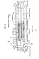
- Figs. 1 to 3 show a first embodiment of a piezoelectric device according to the present invention.
- Fig. 1 is a schematic plan view of the piezoelectric device
- Fig. 2 is a schematic cross-sectional view thereof taken along line II-II in Fig. 1
- Fig. 3 is a sectional end view thereof taken along line III-III in Fig. 1.
- a piezoelectric device 30 constitutes a piezoelectric transducer.
- the piezoelectric device 30 has a vibrating reed housed in a package 37.
- the piezoelectric device 30 has a base substrate 31, a framed vibrating reed 32 that is layered and fixed on the base substrate 31, and a lid 33 that is layered and fixed on the framed vibrating reed 32.
- the package 37 for airtightly housing the vibrating reed is structured so as to include the base substrate 31, the frame of the framed vibrating reed 32, and the lid 33.
- layering the lid 33 on the framed vibrating reed 32 that is layered on the base substrate 31 to adhere the base substrate 31, the framed vibrating reed 32, and the lid 33 to each other forms the package 37.
- the base substrate 31 is the bottom of the package 37.
- the base substrate 31 is formed of an insulating material and is preferably formed of ceramic.
- the base substrate 31 is particularly preferably formed of a material having a thermal expansion coefficient that is equal to or close to the thermal expansion coefficient of the framed vibrating reed 32 or the lid 33 described below.
- the base substrate 31 is formed of a green sheet made of glass ceramic. Shaping a mixture, generated by dispersing ceramic powder in a predetermined solution and adding a binder to the solution, into a long tape and cutting the tape into pieces having a predetermined length provides the green sheet.
- the base substrate 31 is formed of a green sheet produced by mixing glass, forsterite ceramic (2MgO ⁇ SiO 2 ), and a binder.
- the glass ceramic contains the glass component at about 70% and the forsterite component at about 30% by weight in order to provide a thermal expansion coefficient of 13.8 ppm/°C, which is the thermal expansion coefficient of the Z-cut crystal that is used as the material of the framed vibrating reed 32, as described below.
- the glass component contains 80% SiO 2 12% R 2 O (R denotes one Li and/or K), and 8% P 2 O 5 .
- the framed vibrating reed 32 has a vibrating reed body 39 and a frame 36 that surrounds the vibrating reed body 39 in a rectangular shape and that is integrated with the vibrating reed body 39.
- the framed vibrating reed 32 is made of a piezoelectric material, for example, crystal.
- the framed vibrating reed 32 may be made of lithium tantalite or lithium niobate.
- the framed vibrating reed 32 is formed into the shape shown in the drawing by performing wet etching on a wafer, which is Z-cut crystal, by using a hydrofluoric acid solution or by performing dry etching of the wafer.
- the thermal expansion coefficient of the Z-cut crystal is 13.8 ppm/°C.
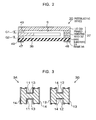
- the vibrating reed body 39 has a plurality of (a pair of, in this embodiment) vibrating arms 34 and 35 that extend rightward from a base 38 integrated with the frame 36 and that are parallel to each other, as shown in Figs. 1 and 2.
- long grooves 11, 11 and 12, 12 that extend in the longitudinal direction of each of the vibrating arms 34 and 35 are formed on the front face and beneath the back face (on the top and underneath, in Fig. 2) of the vibrating arms 34 and 35, respectively.
- Excitation electrodes 13 are formed inside the long grooves 11, 11 of the vibrating arm 34 and excitation electrodes 14 are formed inside the long grooves 12, 12 of the vibrating arm 35.
- the paired excitation electrodes 13 and the paired excitation electrodes 14 extend toward the base 38 and function as heteropolar electrodes with respect to each other.
- the excitation electrodes 13 are formed inside the long grooves 11, 11 of the vibrating arm 34 and the excitation electrodes 14 are formed on opposing side faces of the vibrating arm 34.
- the excitation electrodes 14 are formed in the long grooves 12, 12 of the vibrating arm 35 and the excitation electrodes 13 are formed on opposing side faces of the vibrating arm 35.
- First recesses or cutouts 21, 21 are formed near the base ends of the vibrating arms 34 and 35 in the base 38 of the vibrating reed body 39.
- the first cutouts 21, 21 are formed to narrow the width of the base 38.
- Second recesses or cutouts 22, 22 are formed at the joint where the base 38 is integrally attached to the framed vibrating reed 32.
- the second cutouts 22, 22 are formed to narrow the width of the base 38.
- the first and second cutouts 21 and 22 are simultaneously formed when a crystal wafer is etched to form the outline of the framed vibrating reed 32.
- the excitation electrodes 13 that extend toward the base 38 are lead to the leftward end to provide conductive patterns 13a extending in the width direction of the framed vibrating reed 32.
- the conductive patterns 13a are formed on the front face and beneath the back face of the framed vibrating reed 32.
- the excitation electrodes 14 that extend toward the base 38 are lead to the rightward end through a leading portion 14b along the frame 36 to provide conductive patterns 14a extending in the width direction of the framed vibrating reed 32.
- the conductive patterns 14a are formed on the front face and beneath the back face of the framed vibrating reed 32.
- mounting terminals 47 and 48 are formed at opposing longitudinal ends of the base substrate 31 beneath the back side (bottom) of the base substrate 31.
- cut-away portions 16, 16, 16, 16, which are concaves in the shape of a quarter circle and which extend toward the thickness direction of the piezoelectric device 30, are formed in the four corners of the package 37 in association with the mounting terminals 47 and 48.
- Conductive patterns 16a, 16a, 16a, 16a are formed on the front faces of the cut-away portions 16, 16, 16, 16.
- the excitation electrodes 13 and 14 of the vibrating reed body 39 are electrically connected to the mounting terminals 47 and 48 by making the conductive patterns 13a and 14a and the conductive patterns 16a on the cut-away portions 16 conductive by using a conductive paste or by metallization, including sputtering or plating.
- the electrodes of the framed vibrating reed 32 are formed by sequentially depositing or sputtering, for example, chromium or gold after etching the crystal wafer.
- the electrodes and conductive patterns on the base substrate 31 are formed by applying a conductive paste made of, for example, silver or palladium to the shaped green sheet described above, firing the green sheet, and sequentially plating the fired green sheet with, for example, nickel or gold.
- a conductive paste including a copper paste may be applied on the shaped and fired green sheet and the green sheet may be dried and then plated.
- the lid 33 which is fixed on the framed vibrating reed 32, airtightly seals a space S in which the vibrating reed body 39 is housed.
- the lid 33 is preferably made of a transparent material, such as crystal or glass, which can transmit a laser beam externally radiated for frequency adjustment after the lid 33 is sealed.
- the lid 33 is made of Z-cut crystal, as in the framed vibrating reed 32.
- a transparent material having a thermal expansion coefficient substantially equal to 13.8 ppm/°C, which is the thermal expansion coefficient of the Z-cut crystal is selected.
- Such materials include high-expansion glass, and do not include ordinary soda glass or borosilicate glass. In other words, the component ratio of high-expansion glass is adjusted to set the thermal expansion coefficient of it to 13.8 ppm/°C described above.
- the base substrate 31 is adhered to the framed vibrating reed 32 with a sealing material 49, and the framed vibrating reed 32 is adhered to the lid 33 with another sealing material 49.
- the sealing materials 49, 49 are preferably formed of low-melting glass. Since the sealing materials 49, 49 made of the low-melting glass include filler serving as a spacer, predetermined gaps G1 and G2 are formed on and beneath the vibrating reed body 39 in the space S within the package 37, as shown in Fig. 2. Hence, the vibrating reed body 39 can vibrate as required without trouble, without abutting against the lid 33 or the inner face of the base substrate 31.
- the framed vibrating reed 32 is used and the frame 36 of the framed vibrating reed 32 constitutes a wall around the space S within the package 37.
- the base 38 and the vibrating reed body 39 that includes the pair of vibrating arms 34 and 35 extending from the base 38 are integrally formed inside the frame 36. Accordingly, there is no need to adhere the vibrating reed in the package 37 with an adhesive, thus easily reducing the size of the piezoelectric device 30.
- the vibrating reed body 39 has no structurally weak part such as an extremely narrow connecting part connected to the frame 36, unlike the known vibrating reed described with reference to Fig. 12, and, therefore, the vibrating reed body 39 has no part on which the stress due to an external impact is likely to concentrate and which is apt to be damaged.
- the first cutouts 21, 21 of the base 38 effectively inhibit a vibration leakage from the vibrating arms 34 and 35 from being transmitted to the base 38.
- the second cutouts 22, 22 are formed to narrow the joint between the base 38 and the frame 36 to a width W2.
- the frame 36 defines an external wall of the package 37, any impact due to dropping or the like is strongly exerted on the frame 36.
- the base 38 that has no narrow connecting part, as described above, and that has a relatively large width resists the impact well to prevent the piezoelectric device 30 from being damaged.
- the second cutouts 22, 22 reduce the stress on the frame 36 from the impact transmitted to the vibrating reed body 39.
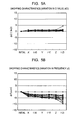
- Fig. 4 is a cross-sectional view taken along line IV-IV in Fig. 1.
- Fig. 4 illustrates the relationship between the frame 36 and forces F, F when an external impact is applied to the frame 36.
- F a force that corresponds to the stress on the frame 36 due to the external impact and that is transmitted to the base 38 having a width W1
- the provision of the second cutouts 22, 22 reduces the force F to a force F2 that is transmitted through the narrowed width W2. That is, since the stress applied to the frame 36 from the external impact is reduced owing to the action of the second cutouts 22, 22 and is transmitted to the base 38, it is possible to effectively prevent the vibrating reed body 39 (refer to Fig. 1) from being damaged.
- Fig. 4 is a drawing for explaining the principle; and the size and scale of each component in Fig. 4 do not exactly coincide with those in Fig. 1.
- the piezoelectric device 30 of the first embodiment can achieve a sufficient impact resistance even when the product is reduced in size.
- the frequency is set to, for example, 30 to 40 kHz and the width W4 of each of the vibrating arms 34 and 35 is set to 50 to 150 ⁇ m.
- the width W2 of the second cutouts 22, 22 is less than 25% of the width W1 of the base 38, the strength is insufficient to attain sufficient impact resistance.
- the width W2 of the second cutouts 22, 22 exceeds 75% of the width W1 of the base 38, the stress due to an impact on the frame 36 transmitted to the vibrating reed body 39 cannot be reduced to a sufficient level.
- the width W1 of the base 38 is preferably less than 500 ⁇ m.
- the width W1 of the base is not less than 500 ⁇ m, it is possible to avoid adhering the electrodes of the base 38 by using conductive adhesives to prevent short-circuiting and, therefore, the structure of the first embodiment is not advantageous.
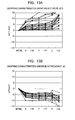
- Fig. 5(a) is a graph showing the variation in CI values of the piezoelectric device 30 in Fig. 1, to which an impact is applied due to dropping.
- Fig. 5(b) is a graph showing the variation in frequency of the piezoelectric device 30 in Fig. 1, to which an impact is applied due to dropping.
- Reference letters X, Y, and Z in Figs. 5(a) and 5(b) denote directions represented by reference letters X, Y, and Z in Fig. 1 and indicate the directions of dropping in the drop test.
- the piezoelectric device 30 has superior impact resistance.
- the piezoelectric device 30 has a CI value approximately equal to 45 k ⁇ (deviation is 2 k ⁇ ), which is the same as CI values of known piezoelectric devices. This is possibly because the frame 36 is integrally adhered to the package 37 and a part that is far away from the vibrating arms 34 and 35 can be fixed, compared with the known vibrating reed of the type shown in Fig. 11.
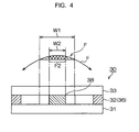
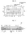
- Figs. 6 and 7 show a second embodiment of a piezoelectric device according to the present invention.
- Fig. 6 is a schematic plan view of the piezoelectric device and
- Fig. 7 is a schematic cross-sectional view thereof taken along line VII-VII in Fig. 6.
- a piezoelectric device 60 of the second embodiment is structured so as to house the framed vibrating reed 32 in the first embodiment in a package 37-1.
- the package 37-1 is a rectangular box.
- a first substrate 51, a second substrate 52, and a third substrate 53 are sequentially layered to form the package 37-1.
- a through-hole 43 is formed near the center of the package 37-1.
- the first substrate 51 and the second substrate 52 constitute a base substrate.
- the through-hole 43 is provided for discharging the gas in the package 37-1 in an annealing treatment during the manufacturing process.
- the through-hole 43 includes a first aperture 44 formed in the first substrate 51 and a second aperture 45 that is formed in the second substrate 52 and that has a diameter smaller than that of the first aperture 44.
- the first aperture 44 communicates with the second aperture 45.
- the through-hole 43 is a stepped hole, as shown in Fig. 7, and is filled with a metal sealing material 46 after the degasification.
- the front surface of the second substrate 52 which is an insulating base, corresponds to the inner surface of the package 37-1. Electrodes 54 and 55 are formed at opposing longitudinal ends of the second substrate 52. The electrodes 54 and 55 are connected to the mounting terminals 47 and 48 through conductive through-holes and 48a, respectively.
- the electrodes 54 and 55 may be connected to the mounting terminals 47 and 48, respectively, in the same manner as in the first embodiment.
- Conductive adhesives 15, 15 are applied to the electrodes 54 and 55.
- Conductive patterns formed on the frame 36 are applied to the conductive adhesives 15, 15 to adhere the conductive patterns to the electrodes 54 and 55.
- the framed vibrating reed 32 has the same structure as in Fig. 1 and is not illustrated in detail in Figs. 6 and 7, the conductive patterns 13a and 14a shown in Fig. 1 are connected to the electrodes 54 and 55, respectively.
- Each of the conductive adhesives 15 is made of, for example, a synthetic resin that serves as an adhesive component (binder component) having an adhesive force and that includes a conductive filler (including conductive particles, such as fine silver particles) and a predetermined solvent.
- the lid 33 is adhered to the package 37-1 with the sealing material 49.
- the piezoelectric device 60 of the second embodiment having the structure described above is slightly larger than the piezoelectric device 30 of the first embodiment because the piezoelectric device 60 houses the framed vibrating reed 32 in the package 37-1.
- the second cutouts 22, 22 inhibit an external impact from being transmitted to the base 38 through the frame 36, as in the first embodiment.
- the piezoelectric device 60 of the second embodiment can basically achieve the same effect as the first embodiment.
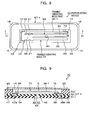
- Figs. 8 and 9 show a third embodiment of a piezoelectric device according to the present invention.
- Fig. 8 is a schematic plan in view of the piezoelectric device and
- Fig. 9 is a schematic cross-sectional view thereof taken along line IX-IX in Fig. 8.
- a piezoelectric device 70 of the third embodiment is structured so as to house a framed vibrating reed 72 in the package 37-1, as in the second embodiment.
- the piezoelectric device 70 of the third embodiment differs from the piezoelectric device 60 of the second embodiment in the structure of the framed vibrating reed 72.
- a framed vibrating reed part 36-1 of the framed vibrating reed 72 is not provided around the vibrating reed body 39, but is formed so as to extend in parallel to the vibrating arms 34 and 35 from the base 38 at one side of the vibrating reed body 39.
- a conductive pattern extending from an excitation electrode (not shown) is provided at a tip 73 of the framed vibrating reed part 36-1. This conductive pattern is similar to the conductive patterns 14a in Fig. 1.
- a conductive pattern (not shown) similar to the conductive pattern 13a in Fig. 1 is provided on the framed vibrating reed part 36-1 at the base 38 side.
- the conductive patterns at the base 38 side and at the tip 73 of the framed vibrating reed part 36-1 are adhered to the electrodes 54 and 55 with the corresponding conductive adhesives 15, 15.
- the piezoelectric device 70 of the third embodiment having the structure described above can achieve the same effect as in the second embodiment. Furthermore, since the framed vibrating reed part 36-1 has a rod-like shape and is provided only at one side of the vibrating arm 34, the mass of the framed vibrating reed part 36-1 is less than the rectangular frame 36 in the second embodiment, thus reducing the damage by any external impact.
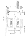
- Fig. 10 is a block diagram schematically showing the structure of a digital cellular phone system as an example of electronic equipment using the piezoelectric device according to any of the above embodiments of the present invention.
- a digital cellular phone system 300 has a microphone 308 for receiving the voice of a caller and a speaker 309 for outputting the received voice.
- the digital cellular phone system 300 further includes a central processing unit (CPU) 301, such as an integrated circuit, functioning as a controller connected to a modem for transmitted and/or received signals.
- CPU central processing unit
- the CPU 301 not only modulates and/or demodulates the transmitted and/or received signals, but also controls a liquid crystal display (LCD) serving as an image display unit, an input-output unit 302 including operation keys for inputting information, and an information storage unit (memory) 303 including a RAM or ROM.
- the piezoelectric device 30, the piezoelectric device 60, the piezoelectric device 70, or the like is connected to the CPU 301, and the output frequency from the piezoelectric device is used as a clock signal appropriate for the control by using a predetermined frequency divider (not shown) included in the CPU 301.
- the piezoelectric device 30 or the like attached to the CPU 301 may be an oscillator having the piezoelectric device 30 or the like combined with a predetermined frequency divider, instead of a simple piezoelectric device.
- the CPU 301 is also connected to a temperature compensated crystal oscillator (TCXO) 305 that is connected to a transmitter unit 307 and a receiver unit 306. Accordingly, even when a basic clock from the CPU 301 is varied due to a change in ambient temperature, the basic clock from the CPU 301 is corrected by the temperature compensated crystal oscillator 305 and the corrected clock is supplied to the transmitter unit 307 and the receiver unit 306.
- TXO temperature compensated crystal oscillator
- the piezoelectric device according to any of the above embodiments can be used in electronic equipment, such as the digital cellular phone system 300 having the controller.
- the piezoelectric device according to any of the above embodiments highly resists an external impact even when it is greatly reduced in size, thus improving the reliability of the product.
- the present invention is not limited to the above embodiments.
- the structures of the above embodiments may be combined with each other or may be combined with other structures, or part of the structures may be omitted.
- the present invention can be applied to any piezoelectric device, regardless of the name, including a piezoelectric transducer or a piezoelectric oscillator, as long as the piezoelectric device has a vibrating reed housed in a package.
Landscapes
- Chemical & Material Sciences (AREA)
- Crystallography & Structural Chemistry (AREA)
- Physics & Mathematics (AREA)
- Acoustics & Sound (AREA)
- Piezo-Electric Or Mechanical Vibrators, Or Delay Or Filter Circuits (AREA)
- Mobile Radio Communication Systems (AREA)
- Apparatuses For Generation Of Mechanical Vibrations (AREA)
- Telephone Function (AREA)
- Telephone Set Structure (AREA)
Applications Claiming Priority (2)
| Application Number | Priority Date | Filing Date | Title |
|---|---|---|---|
| JP2003338558 | 2003-09-29 | ||
| JP2003338558A JP4033100B2 (ja) | 2003-09-29 | 2003-09-29 | 圧電デバイスと圧電デバイスを利用した携帯電話装置および圧電デバイスを利用した電子機器 |
Publications (3)
| Publication Number | Publication Date |
|---|---|
| EP1519484A2 true EP1519484A2 (de) | 2005-03-30 |
| EP1519484A3 EP1519484A3 (de) | 2005-08-17 |
| EP1519484B1 EP1519484B1 (de) | 2008-10-29 |
Family
ID=34191595
Family Applications (1)
| Application Number | Title | Priority Date | Filing Date |
|---|---|---|---|
| EP04022790A Expired - Lifetime EP1519484B1 (de) | 2003-09-29 | 2004-09-24 | Piezoelektrische Vorrichtung, mobiles Telefonsystem und elektronisches Gerät mit der piezoelektrischen Vorrichtung |
Country Status (7)
| Country | Link |
|---|---|
| US (1) | US7067966B2 (de) |
| EP (1) | EP1519484B1 (de) |
| JP (1) | JP4033100B2 (de) |
| KR (1) | KR100659408B1 (de) |
| CN (1) | CN100468967C (de) |
| AT (1) | ATE413016T1 (de) |
| DE (1) | DE602004017392D1 (de) |
Cited By (1)
| Publication number | Priority date | Publication date | Assignee | Title |
|---|---|---|---|---|
| EP2352227A4 (de) * | 2008-09-26 | 2014-04-16 | Daishinku Corp | Piezoelektrisches vibrationsglied des stimmgabeltyps und piezoelektrische vibrationseinrichtung des stimmgabeltyps |
Families Citing this family (43)
| Publication number | Priority date | Publication date | Assignee | Title |
|---|---|---|---|---|
| JP3812724B2 (ja) * | 2001-09-13 | 2006-08-23 | セイコーエプソン株式会社 | 振動片、振動子、発振器及び電子機器 |
| JP4409979B2 (ja) * | 2004-02-10 | 2010-02-03 | シチズンホールディングス株式会社 | 振動子 |
| JP4784168B2 (ja) * | 2005-06-23 | 2011-10-05 | セイコーエプソン株式会社 | 圧電振動片および圧電デバイス |
| JP4442521B2 (ja) | 2005-06-29 | 2010-03-31 | セイコーエプソン株式会社 | 圧電振動片および圧電デバイス |
| JP2007049434A (ja) * | 2005-08-10 | 2007-02-22 | Daishinku Corp | 圧電振動片および圧電振動デバイス |
| JP2007201936A (ja) * | 2006-01-27 | 2007-08-09 | Epson Toyocom Corp | 圧電振動片と圧電デバイス |
| JP2007258918A (ja) * | 2006-03-22 | 2007-10-04 | Epson Toyocom Corp | 圧電デバイス |
| JP5061654B2 (ja) * | 2007-03-02 | 2012-10-31 | 株式会社大真空 | 圧電振動デバイスの製造方法 |
| JP2008233029A (ja) * | 2007-03-23 | 2008-10-02 | Seiko Epson Corp | 加速度センサおよび電子機器 |
| JP2008241547A (ja) * | 2007-03-28 | 2008-10-09 | Seiko Epson Corp | 加速度センサおよび電子機器 |
| US7863803B2 (en) | 2007-05-30 | 2011-01-04 | Epson Toyocom Corporation | Tuning fork resonator element and tuning fork resonator |
| JP4990047B2 (ja) * | 2007-07-02 | 2012-08-01 | 日本電波工業株式会社 | 圧電振動片及び圧電デバイス |
| JP5128262B2 (ja) * | 2007-12-17 | 2013-01-23 | セイコーインスツル株式会社 | 圧電振動片、圧電振動子、発振器、電子機器及び電波時計並びに圧電振動片の製造方法 |
| JP4629094B2 (ja) * | 2007-12-28 | 2011-02-09 | 日本電波工業株式会社 | 圧電振動片、圧電デバイス及びそれらの製造方法 |
| CN101946404A (zh) * | 2008-02-18 | 2011-01-12 | 精工电子有限公司 | 压电振动器的制造方法、压电振动器、振荡器、电子设备及电波钟 |
| WO2009143492A1 (en) * | 2008-05-23 | 2009-11-26 | Statek Corporation | Piezoelectric resonator |
| US8059425B2 (en) * | 2008-05-28 | 2011-11-15 | Azurewave Technologies, Inc. | Integrated circuit module with temperature compensation crystal oscillator |
| JP2010060361A (ja) * | 2008-09-02 | 2010-03-18 | Murata Mfg Co Ltd | 音叉型振動子、音叉型振動子の製造方法および角速度センサ |
| JP4864962B2 (ja) * | 2008-12-17 | 2012-02-01 | 日本電波工業株式会社 | 圧電デバイス |
| JP2011139024A (ja) * | 2009-12-04 | 2011-07-14 | Seiko Epson Corp | パッケージ、および、それを用いた振動デバイス |
| JP5476964B2 (ja) * | 2009-12-09 | 2014-04-23 | セイコーエプソン株式会社 | 振動子、発振器、ジャイロ及び電子機器 |
| US8299863B2 (en) * | 2009-12-25 | 2012-10-30 | Seiko Epson Corporation | Flexural mode resonator element, resonating device, and electronic apparatus |
| JP5148659B2 (ja) * | 2010-05-28 | 2013-02-20 | 日本電波工業株式会社 | 圧電デバイス |
| JP5492671B2 (ja) * | 2010-06-23 | 2014-05-14 | 日本電波工業株式会社 | 圧電デバイス |
| JP5057122B2 (ja) * | 2010-06-25 | 2012-10-24 | セイコーエプソン株式会社 | 圧電振動片および圧電振動子 |
| JP5659585B2 (ja) * | 2010-07-09 | 2015-01-28 | セイコーエプソン株式会社 | 振動片、振動子、発振器及び電子機器 |
| JP5617392B2 (ja) | 2010-07-09 | 2014-11-05 | セイコーエプソン株式会社 | 振動片、振動子及び発振器 |
| JP2012034086A (ja) * | 2010-07-29 | 2012-02-16 | Nippon Dempa Kogyo Co Ltd | 圧電デバイスの製造方法及び圧電デバイス |
| JP2012039509A (ja) * | 2010-08-10 | 2012-02-23 | Seiko Instruments Inc | 圧電振動片、圧電振動子、発振器、電子機器および電波時計 |
| TWI420810B (zh) | 2010-12-17 | 2013-12-21 | Ind Tech Res Inst | 石英振盪器及其製造方法 |
| JP5592812B2 (ja) * | 2011-01-27 | 2014-09-17 | エスアイアイ・クリスタルテクノロジー株式会社 | 圧電振動片、圧電振動子、発振器、電子機器、および電波時計 |
| JP2012169376A (ja) * | 2011-02-10 | 2012-09-06 | Seiko Instruments Inc | 陽極接合装置、パッケージ製造方法、圧電振動子、発振器、電子機器および電波時計 |
| JP5791322B2 (ja) * | 2011-03-28 | 2015-10-07 | セイコーインスツル株式会社 | パッケージの製造方法 |
| JP2013098209A (ja) * | 2011-10-28 | 2013-05-20 | Seiko Epson Corp | 回路基板、電子デバイス、電子機器、及び回路基板の製造方法 |
| JP5911349B2 (ja) * | 2012-03-28 | 2016-04-27 | 京セラクリスタルデバイス株式会社 | 水晶デバイス |
| JP6080486B2 (ja) * | 2012-10-19 | 2017-02-15 | エスアイアイ・クリスタルテクノロジー株式会社 | 圧電振動片、圧電振動子、発振器、電子機器及び電波時計 |
| JP6209886B2 (ja) * | 2013-07-18 | 2017-10-11 | セイコーエプソン株式会社 | 振動片、振動子、発振器、電子機器および移動体 |
| JP6348727B2 (ja) * | 2014-02-14 | 2018-06-27 | エスアイアイ・クリスタルテクノロジー株式会社 | 圧電振動片、圧電振動子、発振器、電子機器、及び電波時計 |
| JP2017011674A (ja) * | 2015-06-25 | 2017-01-12 | 京セラクリスタルデバイス株式会社 | 水晶デバイス |
| JP6548151B2 (ja) * | 2016-10-11 | 2019-07-24 | 株式会社村田製作所 | 圧電振動子及びその製造方法 |
| JP6852569B2 (ja) * | 2017-05-30 | 2021-03-31 | セイコーエプソン株式会社 | Mems素子、電子機器および移動体 |
| JP6816805B2 (ja) * | 2019-10-25 | 2021-01-20 | セイコーエプソン株式会社 | 振動素子、振動子、発振器、電子機器および移動体 |
| WO2022217403A1 (zh) * | 2021-04-12 | 2022-10-20 | 诺思(天津)微系统有限责任公司 | Mems扬声器和电子设备 |
Family Cites Families (15)
| Publication number | Priority date | Publication date | Assignee | Title |
|---|---|---|---|---|
| JPS5323588A (en) | 1976-08-18 | 1978-03-04 | Matsushima Kogyo Kk | Quartz vibrator |
| US4421621A (en) * | 1979-07-17 | 1983-12-20 | Kabushiki Kaisha Suwa Seikosha | Quartz crystal oscillator |
| FR2467487A1 (fr) * | 1979-10-15 | 1981-04-17 | Ebauches Sa | Resonateur piezoelectrique |
| JPS58119218A (ja) | 1982-01-07 | 1983-07-15 | Murata Mfg Co Ltd | 圧電振動装置 |
| JPH09129942A (ja) * | 1995-08-25 | 1997-05-16 | Mitsui Petrochem Ind Ltd | 圧電振動子の支持構造、圧電振動子部品および圧電振動子の実装方法 |
| JP2000031782A (ja) | 1998-07-14 | 2000-01-28 | Toyo Commun Equip Co Ltd | 圧電デバイスの構造 |
| JP4060972B2 (ja) * | 1999-01-29 | 2008-03-12 | セイコーインスツル株式会社 | 圧電振動子及びその製造方法 |
| JP2002261575A (ja) | 2000-12-25 | 2002-09-13 | Seiko Epson Corp | 振動片、振動子、発振器及び電子機器 |
| US6894428B2 (en) * | 2001-01-15 | 2005-05-17 | Seiko Epson Corporation | Vibrating piece, vibrator, oscillator, and electronic device |
| JP3900846B2 (ja) * | 2001-03-02 | 2007-04-04 | セイコーエプソン株式会社 | 音叉型水晶振動片、振動子、発振器及び携帯用電話装置 |
| JP2003069368A (ja) * | 2001-08-22 | 2003-03-07 | Seiko Epson Corp | 圧電デバイスと圧電振動片の接合方法、及び圧電デバイスを利用した携帯電話装置ならびに圧電デバイスを利用した電子機器 |
| US6915548B2 (en) * | 2002-03-06 | 2005-07-12 | Piedek Technical Laboratory | Method for manufacturing quartz crystal tuning fork resonator, quartz crystal unit having quartz crystal tuning fork resonator, and quartz crystal oscillator having quartz crystal unit |
| US6897743B2 (en) * | 2002-03-06 | 2005-05-24 | Piedek Technical Laboratory | Electronic apparatus with two quartz crystal oscillators utilizing different vibration modes |
| JP4001029B2 (ja) * | 2002-03-25 | 2007-10-31 | セイコーエプソン株式会社 | 音叉型圧電振動片及びその製造方法、圧電デバイス |
| KR100476556B1 (ko) * | 2002-04-11 | 2005-03-18 | 삼성전기주식회사 | 압전트랜스 장치, 압전트랜스 하우징 및 그 제조방법 |
-
2003
- 2003-09-29 JP JP2003338558A patent/JP4033100B2/ja not_active Expired - Fee Related
-
2004
- 2004-09-24 AT AT04022790T patent/ATE413016T1/de not_active IP Right Cessation
- 2004-09-24 DE DE602004017392T patent/DE602004017392D1/de not_active Expired - Lifetime
- 2004-09-24 EP EP04022790A patent/EP1519484B1/de not_active Expired - Lifetime
- 2004-09-27 US US10/951,268 patent/US7067966B2/en not_active Expired - Fee Related
- 2004-09-29 CN CNB2004100806870A patent/CN100468967C/zh not_active Expired - Fee Related
- 2004-09-30 KR KR1020040078059A patent/KR100659408B1/ko not_active Expired - Fee Related
Cited By (1)
| Publication number | Priority date | Publication date | Assignee | Title |
|---|---|---|---|---|
| EP2352227A4 (de) * | 2008-09-26 | 2014-04-16 | Daishinku Corp | Piezoelektrisches vibrationsglied des stimmgabeltyps und piezoelektrische vibrationseinrichtung des stimmgabeltyps |
Also Published As
| Publication number | Publication date |
|---|---|
| ATE413016T1 (de) | 2008-11-15 |
| CN1604466A (zh) | 2005-04-06 |
| EP1519484B1 (de) | 2008-10-29 |
| EP1519484A3 (de) | 2005-08-17 |
| KR100659408B1 (ko) | 2006-12-19 |
| CN100468967C (zh) | 2009-03-11 |
| KR20050031445A (ko) | 2005-04-06 |
| DE602004017392D1 (de) | 2008-12-11 |
| JP2005109741A (ja) | 2005-04-21 |
| US7067966B2 (en) | 2006-06-27 |
| US20050104480A1 (en) | 2005-05-19 |
| JP4033100B2 (ja) | 2008-01-16 |
Similar Documents
| Publication | Publication Date | Title |
|---|---|---|
| EP1519484B1 (de) | Piezoelektrische Vorrichtung, mobiles Telefonsystem und elektronisches Gerät mit der piezoelektrischen Vorrichtung | |
| US8692632B2 (en) | Resonator element, resonator, oscillator, and electronic device | |
| JP4281348B2 (ja) | 圧電振動片と圧電振動片を利用した圧電デバイス、ならびに圧電デバイスを利用した携帯電話装置および圧電デバイスを利用した電子機器 | |
| US8020265B2 (en) | Method of manufacturing a piezoelectric vibrator | |
| US8810327B2 (en) | Vibrating member, vibrating device, and electronic apparatus | |
| JP5135510B2 (ja) | 圧電振動子の製造方法、圧電振動子、発振器、電子機器及び電波時計 | |
| US7936114B2 (en) | Piezoelectric vibrator manufacturing method, piezoelectric vibrator, oscillator, electronic device, and radio-controlled watch | |
| US8032997B2 (en) | Manufacturing method for a piezoelectric vibrator | |
| US8058778B2 (en) | Method of manufacturing piezoelectric vibrator, piezoelectric vibrator, oscillator, electronic device, and radio-clock | |
| JP5065494B2 (ja) | 圧電振動子、発振器、電子機器及び電波時計並びに圧電振動子の製造方法 | |
| US20100308928A1 (en) | Piezoelectric vibrator manufacturing method, piezoelectric vibrator, oscillator, electronic device, and radio-controlled watch | |
| JP2003258589A (ja) | 圧電デバイスと圧電デバイスを利用した電波時計、及び圧電デバイスを利用した携帯電話装置ならびに圧電デバイスを利用した電子機器 | |
| WO2009104328A1 (ja) | 圧電振動子の製造方法、圧電振動子、発振器、電子機器及び電波時計 | |
| JP2004120249A (ja) | 圧電振動片と圧電振動片を利用した圧電デバイス、ならびに圧電デバイスを利用した携帯電話装置および圧電デバイスを利用した電子機器 | |
| JP2004201211A (ja) | 圧電振動片の接合構造および圧電デバイスとその製造方法ならびに圧電デバイスを利用した携帯電話装置および圧電デバイスを利用した電子機器 | |
| JP2003198311A (ja) | 圧電デバイスと圧電振動片の接合方法、及び圧電デバイスを利用した携帯電話装置ならびに圧電デバイスを利用した電子機器 | |
| JP6348728B2 (ja) | 圧電振動片、圧電振動子、発振器、電子機器、及び電波時計 | |
| CN104852702B (zh) | 压电振动片、压电振动器、振荡器、电子设备及电波钟表 | |
| JP4020010B2 (ja) | 圧電振動片と圧電振動片を利用した圧電デバイス、ならびに圧電デバイスを利用した携帯電話装置および圧電デバイスを利用した電子機器 | |
| JP4020031B2 (ja) | 圧電振動片と圧電振動片を利用した圧電デバイス、ならびに圧電デバイスを利用した携帯電話装置および圧電デバイスを利用した電子機器 | |
| JP2004222053A (ja) | 圧電デバイス、携帯電話装置及び電子機器 | |
| JP2004336207A (ja) | 圧電振動片と圧電振動片を利用した圧電デバイス、ならびに圧電デバイスを利用した携帯電話装置および圧電デバイスを利用した電子機器 | |
| US20130234565A1 (en) | Piezoelectric vibrator, oscillator, electronic device, and radio-controlled timepiece | |
| JP2005039344A (ja) | 圧電振動片の接合方法および圧電デバイスとその製造方法ならびに圧電デバイスを利用した携帯電話装置および圧電デバイスを利用した電子機器 | |
| JP2005236562A (ja) | 圧電発振器、及びこれを利用した携帯電話装置と電子機器 |
Legal Events
| Date | Code | Title | Description |
|---|---|---|---|
| PUAI | Public reference made under article 153(3) epc to a published international application that has entered the european phase |
Free format text: ORIGINAL CODE: 0009012 |
|
| AK | Designated contracting states |
Kind code of ref document: A2 Designated state(s): AT BE BG CH CY CZ DE DK EE ES FI FR GB GR HU IE IT LI LU MC NL PL PT RO SE SI SK TR |
|
| AX | Request for extension of the european patent |
Extension state: AL HR LT LV MK |
|
| PUAL | Search report despatched |
Free format text: ORIGINAL CODE: 0009013 |
|
| AK | Designated contracting states |
Kind code of ref document: A3 Designated state(s): AT BE BG CH CY CZ DE DK EE ES FI FR GB GR HU IE IT LI LU MC NL PL PT RO SE SI SK TR |
|
| AX | Request for extension of the european patent |
Extension state: AL HR LT LV MK |
|
| 17P | Request for examination filed |
Effective date: 20060213 |
|
| AKX | Designation fees paid |
Designated state(s): AT BE BG CH CY CZ DE DK EE ES FI FR GB GR HU IE IT LI LU MC NL PL PT RO SE SI SK TR |
|
| 17Q | First examination report despatched |
Effective date: 20070809 |
|
| GRAP | Despatch of communication of intention to grant a patent |
Free format text: ORIGINAL CODE: EPIDOSNIGR1 |
|
| GRAS | Grant fee paid |
Free format text: ORIGINAL CODE: EPIDOSNIGR3 |
|
| GRAA | (expected) grant |
Free format text: ORIGINAL CODE: 0009210 |
|
| AK | Designated contracting states |
Kind code of ref document: B1 Designated state(s): AT BE BG CH CY CZ DE DK EE ES FI FR GB GR HU IE IT LI LU MC NL PL PT RO SE SI SK TR |
|
| REG | Reference to a national code |
Ref country code: GB Ref legal event code: FG4D |
|
| REG | Reference to a national code |
Ref country code: CH Ref legal event code: EP |
|
| REG | Reference to a national code |
Ref country code: IE Ref legal event code: FG4D |
|
| REF | Corresponds to: |
Ref document number: 602004017392 Country of ref document: DE Date of ref document: 20081211 Kind code of ref document: P |
|
| NLV1 | Nl: lapsed or annulled due to failure to fulfill the requirements of art. 29p and 29m of the patents act | ||
| PG25 | Lapsed in a contracting state [announced via postgrant information from national office to epo] |
Ref country code: AT Free format text: LAPSE BECAUSE OF FAILURE TO SUBMIT A TRANSLATION OF THE DESCRIPTION OR TO PAY THE FEE WITHIN THE PRESCRIBED TIME-LIMIT Effective date: 20081029 Ref country code: ES Free format text: LAPSE BECAUSE OF FAILURE TO SUBMIT A TRANSLATION OF THE DESCRIPTION OR TO PAY THE FEE WITHIN THE PRESCRIBED TIME-LIMIT Effective date: 20090209 Ref country code: BG Free format text: LAPSE BECAUSE OF FAILURE TO SUBMIT A TRANSLATION OF THE DESCRIPTION OR TO PAY THE FEE WITHIN THE PRESCRIBED TIME-LIMIT Effective date: 20090129 |
|
| PG25 | Lapsed in a contracting state [announced via postgrant information from national office to epo] |
Ref country code: FI Free format text: LAPSE BECAUSE OF FAILURE TO SUBMIT A TRANSLATION OF THE DESCRIPTION OR TO PAY THE FEE WITHIN THE PRESCRIBED TIME-LIMIT Effective date: 20081029 Ref country code: SI Free format text: LAPSE BECAUSE OF FAILURE TO SUBMIT A TRANSLATION OF THE DESCRIPTION OR TO PAY THE FEE WITHIN THE PRESCRIBED TIME-LIMIT Effective date: 20081029 Ref country code: PL Free format text: LAPSE BECAUSE OF FAILURE TO SUBMIT A TRANSLATION OF THE DESCRIPTION OR TO PAY THE FEE WITHIN THE PRESCRIBED TIME-LIMIT Effective date: 20081029 Ref country code: PT Free format text: LAPSE BECAUSE OF FAILURE TO SUBMIT A TRANSLATION OF THE DESCRIPTION OR TO PAY THE FEE WITHIN THE PRESCRIBED TIME-LIMIT Effective date: 20090330 Ref country code: NL Free format text: LAPSE BECAUSE OF FAILURE TO SUBMIT A TRANSLATION OF THE DESCRIPTION OR TO PAY THE FEE WITHIN THE PRESCRIBED TIME-LIMIT Effective date: 20081029 |
|
| PG25 | Lapsed in a contracting state [announced via postgrant information from national office to epo] |
Ref country code: EE Free format text: LAPSE BECAUSE OF FAILURE TO SUBMIT A TRANSLATION OF THE DESCRIPTION OR TO PAY THE FEE WITHIN THE PRESCRIBED TIME-LIMIT Effective date: 20081029 Ref country code: DK Free format text: LAPSE BECAUSE OF FAILURE TO SUBMIT A TRANSLATION OF THE DESCRIPTION OR TO PAY THE FEE WITHIN THE PRESCRIBED TIME-LIMIT Effective date: 20081029 Ref country code: BE Free format text: LAPSE BECAUSE OF FAILURE TO SUBMIT A TRANSLATION OF THE DESCRIPTION OR TO PAY THE FEE WITHIN THE PRESCRIBED TIME-LIMIT Effective date: 20081029 Ref country code: RO Free format text: LAPSE BECAUSE OF FAILURE TO SUBMIT A TRANSLATION OF THE DESCRIPTION OR TO PAY THE FEE WITHIN THE PRESCRIBED TIME-LIMIT Effective date: 20081029 |
|
| PG25 | Lapsed in a contracting state [announced via postgrant information from national office to epo] |
Ref country code: SE Free format text: LAPSE BECAUSE OF FAILURE TO SUBMIT A TRANSLATION OF THE DESCRIPTION OR TO PAY THE FEE WITHIN THE PRESCRIBED TIME-LIMIT Effective date: 20090129 Ref country code: IT Free format text: LAPSE BECAUSE OF FAILURE TO SUBMIT A TRANSLATION OF THE DESCRIPTION OR TO PAY THE FEE WITHIN THE PRESCRIBED TIME-LIMIT Effective date: 20081029 Ref country code: CZ Free format text: LAPSE BECAUSE OF FAILURE TO SUBMIT A TRANSLATION OF THE DESCRIPTION OR TO PAY THE FEE WITHIN THE PRESCRIBED TIME-LIMIT Effective date: 20081029 |
|
| PLBE | No opposition filed within time limit |
Free format text: ORIGINAL CODE: 0009261 |
|
| STAA | Information on the status of an ep patent application or granted ep patent |
Free format text: STATUS: NO OPPOSITION FILED WITHIN TIME LIMIT |
|
| PG25 | Lapsed in a contracting state [announced via postgrant information from national office to epo] |
Ref country code: SK Free format text: LAPSE BECAUSE OF FAILURE TO SUBMIT A TRANSLATION OF THE DESCRIPTION OR TO PAY THE FEE WITHIN THE PRESCRIBED TIME-LIMIT Effective date: 20081029 |
|
| 26N | No opposition filed |
Effective date: 20090730 |
|
| PG25 | Lapsed in a contracting state [announced via postgrant information from national office to epo] |
Ref country code: MC Free format text: LAPSE BECAUSE OF NON-PAYMENT OF DUE FEES Effective date: 20090930 |
|
| REG | Reference to a national code |
Ref country code: CH Ref legal event code: PL |
|
| REG | Reference to a national code |
Ref country code: IE Ref legal event code: MM4A |
|
| REG | Reference to a national code |
Ref country code: FR Ref legal event code: ST Effective date: 20100531 |
|
| PG25 | Lapsed in a contracting state [announced via postgrant information from national office to epo] |
Ref country code: FR Free format text: LAPSE BECAUSE OF NON-PAYMENT OF DUE FEES Effective date: 20090930 Ref country code: IE Free format text: LAPSE BECAUSE OF NON-PAYMENT OF DUE FEES Effective date: 20090924 |
|
| PG25 | Lapsed in a contracting state [announced via postgrant information from national office to epo] |
Ref country code: LI Free format text: LAPSE BECAUSE OF NON-PAYMENT OF DUE FEES Effective date: 20090930 Ref country code: GR Free format text: LAPSE BECAUSE OF FAILURE TO SUBMIT A TRANSLATION OF THE DESCRIPTION OR TO PAY THE FEE WITHIN THE PRESCRIBED TIME-LIMIT Effective date: 20090130 Ref country code: CH Free format text: LAPSE BECAUSE OF NON-PAYMENT OF DUE FEES Effective date: 20090930 |
|
| PG25 | Lapsed in a contracting state [announced via postgrant information from national office to epo] |
Ref country code: LU Free format text: LAPSE BECAUSE OF NON-PAYMENT OF DUE FEES Effective date: 20090924 |
|
| PG25 | Lapsed in a contracting state [announced via postgrant information from national office to epo] |
Ref country code: HU Free format text: LAPSE BECAUSE OF FAILURE TO SUBMIT A TRANSLATION OF THE DESCRIPTION OR TO PAY THE FEE WITHIN THE PRESCRIBED TIME-LIMIT Effective date: 20090430 |
|
| PG25 | Lapsed in a contracting state [announced via postgrant information from national office to epo] |
Ref country code: TR Free format text: LAPSE BECAUSE OF FAILURE TO SUBMIT A TRANSLATION OF THE DESCRIPTION OR TO PAY THE FEE WITHIN THE PRESCRIBED TIME-LIMIT Effective date: 20081029 |
|
| PG25 | Lapsed in a contracting state [announced via postgrant information from national office to epo] |
Ref country code: CY Free format text: LAPSE BECAUSE OF FAILURE TO SUBMIT A TRANSLATION OF THE DESCRIPTION OR TO PAY THE FEE WITHIN THE PRESCRIBED TIME-LIMIT Effective date: 20081029 |
|
| PGFP | Annual fee paid to national office [announced via postgrant information from national office to epo] |
Ref country code: GB Payment date: 20120919 Year of fee payment: 9 |
|
| PGFP | Annual fee paid to national office [announced via postgrant information from national office to epo] |
Ref country code: DE Payment date: 20120919 Year of fee payment: 9 |
|
| GBPC | Gb: european patent ceased through non-payment of renewal fee |
Effective date: 20130924 |
|
| REG | Reference to a national code |
Ref country code: DE Ref legal event code: R119 Ref document number: 602004017392 Country of ref document: DE Effective date: 20140401 |
|
| PG25 | Lapsed in a contracting state [announced via postgrant information from national office to epo] |
Ref country code: GB Free format text: LAPSE BECAUSE OF NON-PAYMENT OF DUE FEES Effective date: 20130924 |
|
| PG25 | Lapsed in a contracting state [announced via postgrant information from national office to epo] |
Ref country code: DE Free format text: LAPSE BECAUSE OF NON-PAYMENT OF DUE FEES Effective date: 20140401 |