EP1521231A2 - Elektronen-Emitter, Bildanzeigeeinrichtung mit Elektronenstrahlerzeugungsgerät und Lichtemittierende Vorrichtung - Google Patents
Elektronen-Emitter, Bildanzeigeeinrichtung mit Elektronenstrahlerzeugungsgerät und Lichtemittierende Vorrichtung Download PDFInfo
- Publication number
- EP1521231A2 EP1521231A2 EP04256108A EP04256108A EP1521231A2 EP 1521231 A2 EP1521231 A2 EP 1521231A2 EP 04256108 A EP04256108 A EP 04256108A EP 04256108 A EP04256108 A EP 04256108A EP 1521231 A2 EP1521231 A2 EP 1521231A2
- Authority
- EP
- European Patent Office
- Prior art keywords
- electrode
- electron
- emitter
- emitter section
- voltage
- Prior art date
- Legal status (The legal status is an assumption and is not a legal conclusion. Google has not performed a legal analysis and makes no representation as to the accuracy of the status listed.)
- Withdrawn
Links
- 239000011521 glass Substances 0.000 claims abstract description 46
- 230000002093 peripheral effect Effects 0.000 claims abstract description 42
- 239000000758 substrate Substances 0.000 claims abstract description 36
- OAICVXFJPJFONN-UHFFFAOYSA-N Phosphorus Chemical compound [P] OAICVXFJPJFONN-UHFFFAOYSA-N 0.000 claims description 37
- 239000003989 dielectric material Substances 0.000 claims description 33
- 230000005684 electric field Effects 0.000 claims description 32
- 239000000126 substance Substances 0.000 claims description 9
- 238000004026 adhesive bonding Methods 0.000 claims description 2
- 238000000034 method Methods 0.000 description 53
- 230000008569 process Effects 0.000 description 44
- 239000003990 capacitor Substances 0.000 description 33
- 239000000463 material Substances 0.000 description 31
- 239000000919 ceramic Substances 0.000 description 23
- 239000010408 film Substances 0.000 description 20
- BASFCYQUMIYNBI-UHFFFAOYSA-N platinum Chemical compound [Pt] BASFCYQUMIYNBI-UHFFFAOYSA-N 0.000 description 20
- 238000009825 accumulation Methods 0.000 description 19
- 238000010586 diagram Methods 0.000 description 19
- 230000010287 polarization Effects 0.000 description 17
- 230000004048 modification Effects 0.000 description 15
- 238000012986 modification Methods 0.000 description 15
- 239000011575 calcium Substances 0.000 description 14
- 238000004519 manufacturing process Methods 0.000 description 11
- 229910052697 platinum Inorganic materials 0.000 description 10
- 230000008859 change Effects 0.000 description 9
- 229910052751 metal Inorganic materials 0.000 description 8
- 239000002184 metal Substances 0.000 description 8
- 229920006395 saturated elastomer Polymers 0.000 description 8
- 150000001875 compounds Chemical class 0.000 description 7
- 238000010304 firing Methods 0.000 description 7
- KDLHZDBZIXYQEI-UHFFFAOYSA-N Palladium Chemical compound [Pd] KDLHZDBZIXYQEI-UHFFFAOYSA-N 0.000 description 6
- NKZSPGSOXYXWQA-UHFFFAOYSA-N dioxido(oxo)titanium;lead(2+) Chemical compound [Pb+2].[O-][Ti]([O-])=O NKZSPGSOXYXWQA-UHFFFAOYSA-N 0.000 description 6
- 238000001962 electrophoresis Methods 0.000 description 6
- 230000006870 function Effects 0.000 description 6
- 239000002245 particle Substances 0.000 description 6
- 238000007667 floating Methods 0.000 description 5
- 239000007789 gas Substances 0.000 description 5
- 230000008018 melting Effects 0.000 description 5
- 238000002844 melting Methods 0.000 description 5
- 239000000203 mixture Substances 0.000 description 5
- ZBSCCQXBYNSKPV-UHFFFAOYSA-N oxolead;oxomagnesium;2,4,5-trioxa-1$l^{5},3$l^{5}-diniobabicyclo[1.1.1]pentane 1,3-dioxide Chemical compound [Mg]=O.[Pb]=O.[Pb]=O.[Pb]=O.O1[Nb]2(=O)O[Nb]1(=O)O2 ZBSCCQXBYNSKPV-UHFFFAOYSA-N 0.000 description 5
- 238000007650 screen-printing Methods 0.000 description 5
- ZOKXTWBITQBERF-UHFFFAOYSA-N Molybdenum Chemical compound [Mo] ZOKXTWBITQBERF-UHFFFAOYSA-N 0.000 description 4
- PXHVJJICTQNCMI-UHFFFAOYSA-N Nickel Chemical compound [Ni] PXHVJJICTQNCMI-UHFFFAOYSA-N 0.000 description 4
- VYPSYNLAJGMNEJ-UHFFFAOYSA-N Silicium dioxide Chemical compound O=[Si]=O VYPSYNLAJGMNEJ-UHFFFAOYSA-N 0.000 description 4
- 238000005229 chemical vapour deposition Methods 0.000 description 4
- 238000009826 distribution Methods 0.000 description 4
- 238000010894 electron beam technology Methods 0.000 description 4
- -1 electrophoresis Substances 0.000 description 4
- 238000002474 experimental method Methods 0.000 description 4
- 150000002500 ions Chemical class 0.000 description 4
- HEPLMSKRHVKCAQ-UHFFFAOYSA-N lead nickel Chemical compound [Ni].[Pb] HEPLMSKRHVKCAQ-UHFFFAOYSA-N 0.000 description 4
- 229910052750 molybdenum Inorganic materials 0.000 description 4
- 239000011733 molybdenum Substances 0.000 description 4
- 229910052712 strontium Inorganic materials 0.000 description 4
- CIOAGBVUUVVLOB-UHFFFAOYSA-N strontium atom Chemical compound [Sr] CIOAGBVUUVVLOB-UHFFFAOYSA-N 0.000 description 4
- 239000000443 aerosol Substances 0.000 description 3
- 229910045601 alloy Inorganic materials 0.000 description 3
- 239000000956 alloy Substances 0.000 description 3
- JRPBQTZRNDNNOP-UHFFFAOYSA-N barium titanate Chemical compound [Ba+2].[Ba+2].[O-][Ti]([O-])([O-])[O-] JRPBQTZRNDNNOP-UHFFFAOYSA-N 0.000 description 3
- 229910002113 barium titanate Inorganic materials 0.000 description 3
- 229910052791 calcium Inorganic materials 0.000 description 3
- 239000011248 coating agent Substances 0.000 description 3
- 238000000576 coating method Methods 0.000 description 3
- 239000012141 concentrate Substances 0.000 description 3
- 230000007423 decrease Effects 0.000 description 3
- 238000000151 deposition Methods 0.000 description 3
- 230000008021 deposition Effects 0.000 description 3
- 238000007598 dipping method Methods 0.000 description 3
- 238000001652 electrophoretic deposition Methods 0.000 description 3
- 229910052746 lanthanum Inorganic materials 0.000 description 3
- FZLIPJUXYLNCLC-UHFFFAOYSA-N lanthanum atom Chemical compound [La] FZLIPJUXYLNCLC-UHFFFAOYSA-N 0.000 description 3
- 239000011572 manganese Substances 0.000 description 3
- 239000010955 niobium Substances 0.000 description 3
- 230000009467 reduction Effects 0.000 description 3
- 230000004044 response Effects 0.000 description 3
- 230000008054 signal transmission Effects 0.000 description 3
- 238000005245 sintering Methods 0.000 description 3
- 239000010409 thin film Substances 0.000 description 3
- WFKWXMTUELFFGS-UHFFFAOYSA-N tungsten Chemical compound [W] WFKWXMTUELFFGS-UHFFFAOYSA-N 0.000 description 3
- 229910052721 tungsten Inorganic materials 0.000 description 3
- 239000010937 tungsten Substances 0.000 description 3
- OYPRJOBELJOOCE-UHFFFAOYSA-N Calcium Chemical compound [Ca] OYPRJOBELJOOCE-UHFFFAOYSA-N 0.000 description 2
- OKTJSMMVPCPJKN-UHFFFAOYSA-N Carbon Chemical compound [C] OKTJSMMVPCPJKN-UHFFFAOYSA-N 0.000 description 2
- FYYHWMGAXLPEAU-UHFFFAOYSA-N Magnesium Chemical compound [Mg] FYYHWMGAXLPEAU-UHFFFAOYSA-N 0.000 description 2
- PWHULOQIROXLJO-UHFFFAOYSA-N Manganese Chemical compound [Mn] PWHULOQIROXLJO-UHFFFAOYSA-N 0.000 description 2
- BQCADISMDOOEFD-UHFFFAOYSA-N Silver Chemical compound [Ag] BQCADISMDOOEFD-UHFFFAOYSA-N 0.000 description 2
- HCHKCACWOHOZIP-UHFFFAOYSA-N Zinc Chemical compound [Zn] HCHKCACWOHOZIP-UHFFFAOYSA-N 0.000 description 2
- 229910052787 antimony Inorganic materials 0.000 description 2
- WATWJIUSRGPENY-UHFFFAOYSA-N antimony atom Chemical compound [Sb] WATWJIUSRGPENY-UHFFFAOYSA-N 0.000 description 2
- 229910052788 barium Inorganic materials 0.000 description 2
- DSAJWYNOEDNPEQ-UHFFFAOYSA-N barium atom Chemical compound [Ba] DSAJWYNOEDNPEQ-UHFFFAOYSA-N 0.000 description 2
- 230000015572 biosynthetic process Effects 0.000 description 2
- CETPSERCERDGAM-UHFFFAOYSA-N ceric oxide Chemical compound O=[Ce]=O CETPSERCERDGAM-UHFFFAOYSA-N 0.000 description 2
- 229910000422 cerium(IV) oxide Inorganic materials 0.000 description 2
- 229910017052 cobalt Inorganic materials 0.000 description 2
- 239000010941 cobalt Substances 0.000 description 2
- GUTLYIVDDKVIGB-UHFFFAOYSA-N cobalt atom Chemical compound [Co] GUTLYIVDDKVIGB-UHFFFAOYSA-N 0.000 description 2
- 229910052681 coesite Inorganic materials 0.000 description 2
- 239000004020 conductor Substances 0.000 description 2
- RKTYLMNFRDHKIL-UHFFFAOYSA-N copper;5,10,15,20-tetraphenylporphyrin-22,24-diide Chemical compound [Cu+2].C1=CC(C(=C2C=CC([N-]2)=C(C=2C=CC=CC=2)C=2C=CC(N=2)=C(C=2C=CC=CC=2)C2=CC=C3[N-]2)C=2C=CC=CC=2)=NC1=C3C1=CC=CC=C1 RKTYLMNFRDHKIL-UHFFFAOYSA-N 0.000 description 2
- 229910052906 cristobalite Inorganic materials 0.000 description 2
- CJXLIMFTIKVMQN-UHFFFAOYSA-N dimagnesium;oxygen(2-);tantalum(5+) Chemical compound [O-2].[O-2].[O-2].[O-2].[O-2].[O-2].[O-2].[Mg+2].[Mg+2].[Ta+5].[Ta+5] CJXLIMFTIKVMQN-UHFFFAOYSA-N 0.000 description 2
- 238000001312 dry etching Methods 0.000 description 2
- 238000005530 etching Methods 0.000 description 2
- 238000001704 evaporation Methods 0.000 description 2
- 230000008020 evaporation Effects 0.000 description 2
- 238000010438 heat treatment Methods 0.000 description 2
- 238000007733 ion plating Methods 0.000 description 2
- 238000010884 ion-beam technique Methods 0.000 description 2
- MRELNEQAGSRDBK-UHFFFAOYSA-N lanthanum(3+);oxygen(2-) Chemical compound [O-2].[O-2].[O-2].[La+3].[La+3] MRELNEQAGSRDBK-UHFFFAOYSA-N 0.000 description 2
- LQBJWKCYZGMFEV-UHFFFAOYSA-N lead tin Chemical compound [Sn].[Pb] LQBJWKCYZGMFEV-UHFFFAOYSA-N 0.000 description 2
- JQJCSZOEVBFDKO-UHFFFAOYSA-N lead zinc Chemical compound [Zn].[Pb] JQJCSZOEVBFDKO-UHFFFAOYSA-N 0.000 description 2
- 239000004973 liquid crystal related substance Substances 0.000 description 2
- 229910052749 magnesium Inorganic materials 0.000 description 2
- 239000011777 magnesium Substances 0.000 description 2
- 229910052748 manganese Inorganic materials 0.000 description 2
- WPBNNNQJVZRUHP-UHFFFAOYSA-L manganese(2+);methyl n-[[2-(methoxycarbonylcarbamothioylamino)phenyl]carbamothioyl]carbamate;n-[2-(sulfidocarbothioylamino)ethyl]carbamodithioate Chemical compound [Mn+2].[S-]C(=S)NCCNC([S-])=S.COC(=O)NC(=S)NC1=CC=CC=C1NC(=S)NC(=O)OC WPBNNNQJVZRUHP-UHFFFAOYSA-L 0.000 description 2
- 239000011159 matrix material Substances 0.000 description 2
- 230000003446 memory effect Effects 0.000 description 2
- QSHDDOUJBYECFT-UHFFFAOYSA-N mercury Chemical compound [Hg] QSHDDOUJBYECFT-UHFFFAOYSA-N 0.000 description 2
- 229910052753 mercury Inorganic materials 0.000 description 2
- 229910052759 nickel Inorganic materials 0.000 description 2
- 229910052758 niobium Inorganic materials 0.000 description 2
- GUCVJGMIXFAOAE-UHFFFAOYSA-N niobium atom Chemical compound [Nb] GUCVJGMIXFAOAE-UHFFFAOYSA-N 0.000 description 2
- 229910052763 palladium Inorganic materials 0.000 description 2
- 238000007747 plating Methods 0.000 description 2
- 239000004065 semiconductor Substances 0.000 description 2
- 238000004904 shortening Methods 0.000 description 2
- 239000000377 silicon dioxide Substances 0.000 description 2
- 229910052709 silver Inorganic materials 0.000 description 2
- 239000004332 silver Substances 0.000 description 2
- 238000004544 sputter deposition Methods 0.000 description 2
- 229910052682 stishovite Inorganic materials 0.000 description 2
- 229910052905 tridymite Inorganic materials 0.000 description 2
- 238000007738 vacuum evaporation Methods 0.000 description 2
- 238000001039 wet etching Methods 0.000 description 2
- 229910052725 zinc Inorganic materials 0.000 description 2
- 239000011701 zinc Substances 0.000 description 2
- 239000004925 Acrylic resin Substances 0.000 description 1
- 229920000178 Acrylic resin Polymers 0.000 description 1
- 229910001316 Ag alloy Inorganic materials 0.000 description 1
- BHPQYMZQTOCNFJ-UHFFFAOYSA-N Calcium cation Chemical compound [Ca+2] BHPQYMZQTOCNFJ-UHFFFAOYSA-N 0.000 description 1
- 229910002269 La1–xCaxMnO3 Inorganic materials 0.000 description 1
- 229910002273 La1–xSrxCoO3 Inorganic materials 0.000 description 1
- 229910003781 PbTiO3 Inorganic materials 0.000 description 1
- 229910020698 PbZrO3 Inorganic materials 0.000 description 1
- 229910001252 Pd alloy Inorganic materials 0.000 description 1
- 229910002353 SrRuO3 Inorganic materials 0.000 description 1
- 238000010521 absorption reaction Methods 0.000 description 1
- 239000000654 additive Substances 0.000 description 1
- 230000000996 additive effect Effects 0.000 description 1
- 230000003321 amplification Effects 0.000 description 1
- XDFCIPNJCBUZJN-UHFFFAOYSA-N barium(2+) Chemical compound [Ba+2] XDFCIPNJCBUZJN-UHFFFAOYSA-N 0.000 description 1
- 229910000416 bismuth oxide Inorganic materials 0.000 description 1
- 239000005388 borosilicate glass Substances 0.000 description 1
- 229910052799 carbon Inorganic materials 0.000 description 1
- 230000001413 cellular effect Effects 0.000 description 1
- 239000011195 cermet Substances 0.000 description 1
- 238000004891 communication Methods 0.000 description 1
- 239000002131 composite material Substances 0.000 description 1
- 239000000470 constituent Substances 0.000 description 1
- TYIXMATWDRGMPF-UHFFFAOYSA-N dibismuth;oxygen(2-) Chemical compound [O-2].[O-2].[O-2].[Bi+3].[Bi+3] TYIXMATWDRGMPF-UHFFFAOYSA-N 0.000 description 1
- HTXDPTMKBJXEOW-UHFFFAOYSA-N dioxoiridium Chemical compound O=[Ir]=O HTXDPTMKBJXEOW-UHFFFAOYSA-N 0.000 description 1
- IVUXZQJWTQMSQN-UHFFFAOYSA-N distrontium;oxygen(2-);tantalum(5+) Chemical compound [O-2].[O-2].[O-2].[O-2].[O-2].[O-2].[O-2].[Sr+2].[Sr+2].[Ta+5].[Ta+5] IVUXZQJWTQMSQN-UHFFFAOYSA-N 0.000 description 1
- 238000001035 drying Methods 0.000 description 1
- 239000007772 electrode material Substances 0.000 description 1
- 238000005566 electron beam evaporation Methods 0.000 description 1
- 239000012776 electronic material Substances 0.000 description 1
- 239000000839 emulsion Substances 0.000 description 1
- 229910002804 graphite Inorganic materials 0.000 description 1
- 239000010439 graphite Substances 0.000 description 1
- 238000009396 hybridization Methods 0.000 description 1
- 239000000976 ink Substances 0.000 description 1
- 229910052741 iridium Inorganic materials 0.000 description 1
- GKOZUEZYRPOHIO-UHFFFAOYSA-N iridium atom Chemical compound [Ir] GKOZUEZYRPOHIO-UHFFFAOYSA-N 0.000 description 1
- 230000001788 irregular Effects 0.000 description 1
- HFGPZNIAWCZYJU-UHFFFAOYSA-N lead zirconate titanate Chemical compound [O-2].[O-2].[O-2].[O-2].[O-2].[Ti+4].[Zr+4].[Pb+2] HFGPZNIAWCZYJU-UHFFFAOYSA-N 0.000 description 1
- RVPVRDXYQKGNMQ-UHFFFAOYSA-N lead(2+) Chemical compound [Pb+2] RVPVRDXYQKGNMQ-UHFFFAOYSA-N 0.000 description 1
- 239000007788 liquid Substances 0.000 description 1
- 230000007246 mechanism Effects 0.000 description 1
- MYWUZJCMWCOHBA-VIFPVBQESA-N methamphetamine Chemical compound CN[C@@H](C)CC1=CC=CC=C1 MYWUZJCMWCOHBA-VIFPVBQESA-N 0.000 description 1
- 238000005459 micromachining Methods 0.000 description 1
- 238000003199 nucleic acid amplification method Methods 0.000 description 1
- 230000001590 oxidative effect Effects 0.000 description 1
- 238000005268 plasma chemical vapour deposition Methods 0.000 description 1
- 229920003217 poly(methylsilsesquioxane) Polymers 0.000 description 1
- 239000010970 precious metal Substances 0.000 description 1
- 238000002360 preparation method Methods 0.000 description 1
- 238000007639 printing Methods 0.000 description 1
- 238000012552 review Methods 0.000 description 1
- 229910052703 rhodium Inorganic materials 0.000 description 1
- 239000010948 rhodium Substances 0.000 description 1
- MHOVAHRLVXNVSD-UHFFFAOYSA-N rhodium atom Chemical compound [Rh] MHOVAHRLVXNVSD-UHFFFAOYSA-N 0.000 description 1
- WOCIAKWEIIZHES-UHFFFAOYSA-N ruthenium(iv) oxide Chemical compound O=[Ru]=O WOCIAKWEIIZHES-UHFFFAOYSA-N 0.000 description 1
- 239000002002 slurry Substances 0.000 description 1
- 125000006850 spacer group Chemical group 0.000 description 1
- 238000005507 spraying Methods 0.000 description 1
- PWYYWQHXAPXYMF-UHFFFAOYSA-N strontium(2+) Chemical compound [Sr+2] PWYYWQHXAPXYMF-UHFFFAOYSA-N 0.000 description 1
- 239000000725 suspension Substances 0.000 description 1
- 235000012431 wafers Nutrition 0.000 description 1
Images


Classifications
-
- H—ELECTRICITY
- H01—ELECTRIC ELEMENTS
- H01J—ELECTRIC DISCHARGE TUBES OR DISCHARGE LAMPS
- H01J1/00—Details of electrodes, of magnetic control means, of screens, or of the mounting or spacing thereof, common to two or more basic types of discharge tubes or lamps
- H01J1/02—Main electrodes
- H01J1/30—Cold cathodes, e.g. field-emissive cathode
- H01J1/312—Cold cathodes, e.g. field-emissive cathode having an electric field perpendicular to the surface, e.g. tunnel-effect cathodes of metal-insulator-metal [MIM] type
-
- B—PERFORMING OPERATIONS; TRANSPORTING
- B82—NANOTECHNOLOGY
- B82Y—SPECIFIC USES OR APPLICATIONS OF NANOSTRUCTURES; MEASUREMENT OR ANALYSIS OF NANOSTRUCTURES; MANUFACTURE OR TREATMENT OF NANOSTRUCTURES
- B82Y10/00—Nanotechnology for information processing, storage or transmission, e.g. quantum computing or single electron logic
-
- H—ELECTRICITY
- H01—ELECTRIC ELEMENTS
- H01J—ELECTRIC DISCHARGE TUBES OR DISCHARGE LAMPS
- H01J31/00—Cathode ray tubes; Electron beam tubes
- H01J31/08—Cathode ray tubes; Electron beam tubes having a screen on or from which an image or pattern is formed, picked up, converted, or stored
- H01J31/10—Image or pattern display tubes, i.e. having electrical input and optical output; Flying-spot tubes for scanning purposes
- H01J31/12—Image or pattern display tubes, i.e. having electrical input and optical output; Flying-spot tubes for scanning purposes with luminescent screen
- H01J31/123—Flat display tubes
- H01J31/125—Flat display tubes provided with control means permitting the electron beam to reach selected parts of the screen, e.g. digital selection
- H01J31/127—Flat display tubes provided with control means permitting the electron beam to reach selected parts of the screen, e.g. digital selection using large area or array sources, i.e. essentially a source for each pixel group
-
- H—ELECTRICITY
- H01—ELECTRIC ELEMENTS
- H01J—ELECTRIC DISCHARGE TUBES OR DISCHARGE LAMPS
- H01J63/00—Cathode-ray or electron-stream lamps
- H01J63/02—Details, e.g. electrode, gas filling, shape of vessel
-
- G—PHYSICS
- G09—EDUCATION; CRYPTOGRAPHY; DISPLAY; ADVERTISING; SEALS
- G09G—ARRANGEMENTS OR CIRCUITS FOR CONTROL OF INDICATING DEVICES USING STATIC MEANS TO PRESENT VARIABLE INFORMATION
- G09G2310/00—Command of the display device
- G09G2310/06—Details of flat display driving waveforms
-
- G—PHYSICS
- G09—EDUCATION; CRYPTOGRAPHY; DISPLAY; ADVERTISING; SEALS
- G09G—ARRANGEMENTS OR CIRCUITS FOR CONTROL OF INDICATING DEVICES USING STATIC MEANS TO PRESENT VARIABLE INFORMATION
- G09G3/00—Control arrangements or circuits, of interest only in connection with visual indicators other than cathode-ray tubes
- G09G3/20—Control arrangements or circuits, of interest only in connection with visual indicators other than cathode-ray tubes for presentation of an assembly of a number of characters, e.g. a page, by composing the assembly by combination of individual elements arranged in a matrix no fixed position being assigned to or needed to be assigned to the individual characters or partial characters
- G09G3/22—Control arrangements or circuits, of interest only in connection with visual indicators other than cathode-ray tubes for presentation of an assembly of a number of characters, e.g. a page, by composing the assembly by combination of individual elements arranged in a matrix no fixed position being assigned to or needed to be assigned to the individual characters or partial characters using controlled light sources
-
- H—ELECTRICITY
- H01—ELECTRIC ELEMENTS
- H01J—ELECTRIC DISCHARGE TUBES OR DISCHARGE LAMPS
- H01J2201/00—Electrodes common to discharge tubes
- H01J2201/30—Cold cathodes
- H01J2201/312—Cold cathodes having an electric field perpendicular to the surface thereof
- H01J2201/3125—Metal-insulator-Metal [MIM] emission type cathodes
Definitions
- the present invention relates to an electron emitter formed on a glass substrate, an electron emission device including a plurality of the electron emitters, a display using the electron emission device, and a light source using the electron emission device.
- FEDs field emission displays
- backlight units In recent years, electron emitters having a cathode electrode and an anode electrode have been used in various applications such as field emission displays (FEDs) and backlight units.
- FEDs field emission displays
- a plurality of electron emitters are arranged in a two-dimensional array, and a plurality of phosphors are positioned at predetermined intervals in association with the respective electron emitters.
- an upper electrode 204 and a lower electrode 206 are formed on an emitter section 202 in a conventional electron emitter 200, the upper electrode 204 in particular is formed in intimate contact with the emitter 202.
- a point where electric field concentrates is a triple point made up of the upper electrode 204, the emitter 202, and the vacuum, and corresponds to a peripheral edge portion of the upper electrode 204.
- the peripheral edge portion of the upper electrode 204 is in intimate contact with the emitter 202, the degree of electric field concentration is small and the energy required to emit electrons is large. Furthermore, because an electron emission region is limited to the peripheral edge portion of the upper electrode 204, the overall electron emission characteristics tend to vary, making it difficult to control the emission of electrons and also making the electron emission efficiency low.
- the present invention has been made in view of the above drawbacks.
- another object of the present invention is to provide a display and a light source with high luminance at low cost using an electron emission device having advantages in producing a large panel and reducing the production cost, in which electrons are emitted highly efficiently with a large output at a low voltage.
- an electron emitter comprises a first electrode formed on a glass substrate, an emitter section made of a dielectric film formed on the first electrode, and a second electrode formed on the emitter section.
- a drive voltage for electron emission is applied between the first electrode and the second electrode.
- At least the second electrode has a plurality of through regions through which the emitter section is exposed.
- the second electrode has a surface which faces the emitter section in peripheral portions of the through regions and which is spaced from the emitter section.
- an electron emission device includes a plurality of electron emitters formed on a glass substrate.
- Each of the electron emitters comprises a first electrode formed on the glass substrate, an emitter section made of a dielectric film formed on the first electrode, a second electrode formed on the emitter section.
- a drive voltage for electron emission is applied between the first electrode and the second electrode, at least the second electrode has a plurality of through regions through which the emitter section is exposed.
- the second electrode has a surface which faces the emitter section in peripheral portions of the through regions and which is spaced from the emitter section.
- a display comprises the above electron emission device.
- the display further comprises a transparent plate provided on a surface of the glass substrate facing the emitter section of the electron emission device, an electrode formed on a surface of the transparent plate facing the emitter section for generating an electric field between the electrode and the electron emitter of the electron emission device, and a phosphor formed on the electrode.
- the phosphor is energized to emit light when electrons emitted from the electron emitter impinge on the phosphor.
- a light source comprises the above electron emission device.
- the light source further comprises a transparent plate provided on a surface of the glass substrate facing the emitter section of the electron emission device, an electrode formed on a surface of the transparent plate facing the emitter section for generating an electric field between the electrode and the electron emitter of the electron emission device, and a phosphor formed on the electrode.
- the phosphor is energized to emit light when electrons emitted from the electron emitter impinge on the phosphor.
- a drive voltage is applied between the first electrode and the second electrode.
- the drive voltage is defined as a voltage, such as a pulse voltage or an alternating-current voltage, which abruptly changes, with time, from a voltage level higher or lower than a reference voltage (e.g., 0 V) to a voltage level that is lower or higher than the reference voltage.
- a reference voltage e.g. 0 V
- a triple junction is formed in a region of contact between a surface on which the second electrode is formed, the second electrode, and a medium (e.g., a vacuum) around the electron emitter.
- the triple junction is defined as an electric field concentration region formed by a contact between the second electrode, the emitter section, and the vacuum.
- the triple junction includes a triple point where the second electrode, the emitter section, and the vacuum exist as one point.
- the triple junction is formed the peripheral portions of the through regions and the peripheral area of the second electrode. Therefore, when the drive voltage is applied between the first electrode and the second electrode, an electric field concentration occurs at the triple junction.
- the voltage higher or lower than the reference voltage is applied between the first electrode and the second electrode, producing an electric field concentration in one direction, for example, at the triple junction and/or the tip of the second electrode. Electrons are emitted from the second electrode toward the emitter section, and accumulated in the portions of the emitter section which correspond to the through regions of the second electrode and the portion of the emitter section near the peripheral portion of the second electrode. That is, the emitter section is charged. At this time, the second electrode functions as an electron supply source.
- the voltage level of the drive voltage abruptly changes, i.e., the voltage lower or higher than the reference voltage is applied between the first electrode and the second electrode.
- the electrons that have been accumulated in the portions corresponding to the through regions of the second electrode and the regions near the peripheral portion of the second electrode are expelled from the emitter section by dipoles (whose negative poles appear on the surface of the emitter section) in the emitter section whose polarization has been reversed in the opposite direction.
- the electrons are emitted from the portions of the emitter section where the electrons have been accumulated, through the through regions.
- the electrons are also emitted from the regions near the outer peripheral portion of the second electrode.
- electrons in correspondence with the amount of charges in the emitter section in the first stage are emitted from the emitter section in the second stage.
- the amount of charges in the emitter section in the first stage is maintained until electrons are emitted in the second stage.
- the electron emitter in a first output period, is prepared for electron emission (e.g., the emitter section is polarized in one direction).
- a next second output period when the voltage level of the drive voltage is quickly changed, an electric field concentration occurs at the triple junction and/or the tip of the second electrode, causing the second electrode to emit primary electrons, which impinge upon the portions of the emitter section which are exposed through the through regions and the regions near the outer peripheral portion of the second electrode.
- Secondary electrons (including reflected primary electrons) are emitted from the portions hit by the primary electrons.
- secondary electrons are emitted from the through regions and the regions near the outer peripheral portion of the second electrode in an initial stage of the second output period.
- the second electrode of the electron emitter has the through regions, electrons are uniformly emitted from each of the through regions and the outer peripheral portions of the second electrode. Thus, any variations in the overall electron emission characteristics of the electron emitter are reduced, making it possible to facilitate the control of the electron emission and increase the electron emission efficiency.
- the present invention furthermore, because a gap is formed between the surface of the second electrode which faces the emitter section in the peripheral portions of the through regions and the emitter section, when the drive voltage is applied, an electric field concentration tends to be produced in the region of the gap. This leads to a higher efficiency of the electron emission, making the drive voltage lower (emitting electrons at a lower voltage level).
- the gap is formed between the surface of the second electrode which faces the emitter section in the peripheral portions of the through regions and the emitter section, providing overhanging portions (flanges) on the peripheral portions of the through regions, electrons are easily emitted from the overhanging portions (the peripheral portions of the through regions) of the second electrode, also with the increased electric field concentration in the region of the gap. This leads to a larger output and higher efficiency of the electron emission, making the drive voltage lower.
- the straightness of emitted electrons can be increased. This is effective in reducing crosstalk if electron emitters are arrayed for use as an electron source of a display.
- the electron emitter according to aspects of the present invention is capable of easily developing a high electric field concentration, provides many electron emission regions, has a larger output and higher efficiency of the electron emission, and can be driven at a lower voltage (lower power consumption).
- the glass substrate since the glass substrate is employed, it is possible to produce a large panel, and reduce the production cost. Further, it is possible to lower the process temperature for producing the electron emitter, and lower the cost for facilities. Crystallized glass may be used for the glass substrate. In this case, unlike the normal glass, since the process temperature is in a range from 600 to 800°c, selection of the material can be carried out freely.
- the glass plate Since the glass plate is employed, it is possible to produce a large panel corresponding to a back light for a large screen display or a large screen liquid display. Further, when a vacuum tube hermetically containing the electron emitter is fabricated, a tube wall and a spacer, or a transparent plate forming a phosphor may be made of glass, and these components can be adhered to the glass substrate, using a frit, on which the electron emitter is formed. Conversely, when the electron emitter is formed on a substrate which is not made of glass, since the thermal expansion coefficient of the other glass members and the thermal expansion coefficient of the frit do not match, the tube fabrication is difficult.
- At least a surface of emitter section for forming the second electrode may have surface irregularities due to the grain boundary of the dielectric material, and the through regions of the second electrode may be formed in regions corresponding to concavities of the surface irregularities due to the grain boundary of the dielectric material.
- the second electrode may be in the form of a cluster of a plurality of scale-like substances or a cluster of a plurality of electrically conductive substances including scale-like substances.
- second electrode has a surface which faces the emitter section in peripheral portions of the through regions and which is spaced from the emitter section, i.e., the structure where a gap is formed between the surface of the second electrode which faces the emitter section in the peripheral portions of the through regions and the emitter section.
- the electron emitter and the electron emission device are capable of easily developing a high electric field concentration, provides many electron emission regions, has a larger output and higher efficiency of the electron emission, and can be driven at a lower voltage (lower power consumption).
- the electron emitter and the electron emission device are advantageous in producing a large panel and reducing the production cost.
- the display and the light source according to aspects of the present invention have a large screen or large area, and high luminance.
- the display and light source can be produced at low cost.
- Electron emitters according to the present invention can be used in electron beam irradiation apparatus, light sources, alternative to LEDs, electronic parts manufacturing apparatus, and electronic circuit components, as well as display applications.
- An electron beam in an electron beam irradiation apparatus has a higher energy and a better absorption capability than ultraviolet rays in ultraviolet ray irradiation apparatus that are presently in widespread use.
- the electron emitters may be used to solidify insulating films in superposing wafers for semiconductor devices, harden printing inks without irregularities for drying prints, and sterilize medical devices while being kept in packages.
- the electron emitters may be used as surface light sources such as backlight units for liquid crystal displays. ⁇ The electron emitters may also be used as high-luminance, high-efficiency light sources for use in projectors, for example, which may employ ultrahigh-pressure mercury lamps.
- the light source using the electron emitters according to the present embodiment is compact, has a long service life, and has a high-speed turn-on capability.
- the electron emitter does not use any mercury, and the electron emitter is environmentally friendly.
- the electron emitters may also be used as alternatives to LEDs, such as surface light sources for indoor lights, automobile lamps, surface light sources for traffic signal devices, chip light sources, and backlight units for traffic signal devices, small-size liquid-crystal display devices for cellular phones.
- the electron emitters may also be used in electronic parts manufacturing apparatus as electron beam sources for film growing apparatus such as electron beam evaporation apparatus, electron sources for generating a plasma (to activate a gas or the like) in plasma CVD apparatus, and electron sources for decomposing gases. Electron emitters may also be used in vacuum micro devices including ultrahigh-speed devices operable in a tera-Hz range and large-current output devices. Electron emitters may also preferably be used as printer components, i.e., light emission devices for applying light to a photosensitive drum in combination with a phosphor, and electron sources for charging dielectric materials.
- the electron emitters may also be used in electronic circuit components including digital devices such as switches, relays, diodes, etc. and analog devices such as operational amplifiers, etc. as they can be designed for outputting large currents and higher amplification factors.
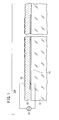
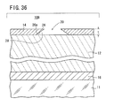
- an electron emitter 10A is formed on a glass substrate 11.
- the electron emitter 10A includes a plate-like emitter section 12 made of a dielectric material, a first electrode (e.g., a lower electrode) 16 formed on a first surface (e.g., a lower surface) of the emitter section 12, a second electrode (e.g., an upper electrode) 14 formed on a second surface (e.g., an upper surface) of the emitter section 12, and a pulse generation source 18 for applying a drive voltage Va between the upper electrode 14 and the lower electrode 16.
- a first electrode e.g., a lower electrode
- a second electrode e.g., an upper electrode
- a pulse generation source 18 for applying a drive voltage Va between the upper electrode 14 and the lower electrode 16.
- the upper electrode 14 has a plurality of through regions 20 where the emitter section 12 is exposed.
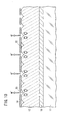
- the emitter section 12 has surface irregularities 22 due to the grain boundary of the dielectric material.
- the through regions 20 of the upper electrode 14 are formed in areas corresponding to concavities 24 due to the grain boundary of the dielectric material.
- one through region 20 is formed in association with one recess 24.
- one through region 20 may be formed in association with a plurality of concavities 24.
- the particle diameter of the dielectric material of the emitter section 12 should preferably be in the range from 0.1 ⁇ m to 10 ⁇ m, and more preferably be in the range from 2 ⁇ m to 7 ⁇ m. In the example shown in FIG. 2, the particle diameter of the dielectric material is of 3 ⁇ m.
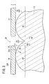
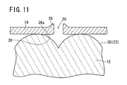
- each of the through regions 20 of the upper electrode 12 has a peripheral portion 26 having a surface 26a facing the emitter section 12.
- the surface 26a is spaced from the emitter section 12.
- a gap 28 is formed between the surface 26a, facing the emitter section 12, of the peripheral portion 26 of the through region 20 and the emitter section 12, and the peripheral portion 26 of the through region 20 of the upper electrode 14 is formed as an overhanging portion (flange).
- the peripheral portion 26 of the through region 20 of the upper electrode 14 is referred to as "the overhanging portion 26 of the upper electrode 14".
- convexities 30 of the surface irregularities 22 of the grain boundary of the dielectric material are shown as having a semicircular cross-sectional shape.
- the convexities 30 are not limited to the semicircular cross-sectional shape.
- the upper electrode 14 has a thickness t in the range of 0.01 ⁇ m ⁇ t ⁇ 10 ⁇ m, and the maximum angle ⁇ between the upper surface of the emitter section 12, i.e., the surface of the convexity 30 (which is also the inner wall surface of the concavity 24) of the grain boundary of the dielectric material, and the lower surface 26a of the overhanging portion 26 of the upper electrode 14 is in the range of 1° ⁇ ⁇ ⁇ 60°.
- the maximum distance d in the vertical direction between the surface of the convexity 30 (the inner wall surface of the concavity 24) of the grain boundary of the dielectric material and the lower surface 26a of the overhanging portion 26 of the upper electrode 14 is in the range of 0 ⁇ m ⁇ d ⁇ 10 ⁇ m.
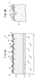
- the shape of the through region 20, particularly the shape as seen from above, as shown in FIG. 4, is the shape of a hole 32.
- the shape of the hole 32 may be a circular shape, an elliptical shape, a track shape, and may include a curve, or a polygonal shape such as a quadrangular shape or a triangular shape.
- the shape of the hole 32 is a circular shape.
- the hole 32 has an average diameter ranging from 0.1 ⁇ m to 10 ⁇ m.
- the average diameter represents the average of the lengths of a plurality of different line segments passing through the center of the hole 32.
- the dielectric material which the emitter section 12 is made of may be a dielectric material having a relatively large dielectric constant, e.g., a dielectric constant of 1000 or larger.
- Dielectric materials of such a nature may be ceramics including barium titanate, lead zirconate, lead magnesium niobate, lead nickel niobate, lead zinc niobate, lead manganese niobate, lead magnesium tantalate, lead nickel tantalate, lead antimony tinate, lead titanate, lead magnesium tungstenate, lead cobalt niobate, etc.
- any of these materials a material which chiefly contains 50 weight % or more of any of these materials, or such ceramics to which there is added an oxide such as lanthanum, calcium, strontium, molybdenum, tungsten, barium, niobium, zinc, nickel, manganese, or the like, or a combination of these materials, or any of other compounds.
- nPMN-mPT nPMN-mPT
- PT lead titanate
- MPB morphotropic phase boundary
- a dielectric material may be mixed with 20 weight % of platinum.
- the emitter section 12 may be in the form of a piezoelectric/electrostrictive layer or an anti-ferroelectric layer. If the emitter section 12 comprises a piezoelectric/electrostrictive layer, then it may be made of ceramics such as lead zirconate, lead magnesium niobate, lead nickel niobate, lead zinc niobate, lead manganese niobate, lead magnesium tantalate, lead nickel tantalate, lead antimony tinate, lead titanate, barium titanate, lead magnesium tungstenate, lead cobalt niobate, or the like. or a combination of any of these materials.
- ceramics such as lead zirconate, lead magnesium niobate, lead nickel niobate, lead zinc niobate, lead manganese niobate, lead magnesium tantalate, lead nickel tantalate, lead antimony tinate, lead titanate, barium titanate, lead magnesium tungstenate,
- the emitter section 12 may be made of chief components including 50 wt % or more of any of the above compounds. Of the above ceramics, the ceramics including lead zirconate is mostly frequently used as a constituent of the piezoelectric/electrostrictive layer of the emitter section 12.
- the piezoelectric/electrostrictive layer is made of ceramics, then lanthanum, calcium, strontium, molybdenum, tungsten, barium, niobium, zinc, nickel, manganese, or the like, or a combination of these materials, or any of other compounds may be added to the ceramics.
- ceramics produced by adding SiO 2 , CeO 2 , Pb 5 Ge 3 O 11 , or a combination of any of these compounds to the above ceramics may be used.
- a material produced by adding 0.2 wt % of SiO 2 , 0.1 wt % of CeO 2 , or 1 to 2 wt % of Pb 5 Ge 3 O 11 to a PT-PZ-PMN piezoelectric material is preferable.
- the piezoelectric/electrostrictive layer should preferably be made of ceramics including as chief components lead magnesium niobate, lead zirconate, and lead titanate, and also including lanthanum and strontium.
- the piezoelectric/electrostrictive layer may be dense or porous. If the piezoelectric/electrostrictive layer is porous, then it should preferably have a porosity of 40 % or less.
- the anti-ferroelectric layer may be made of lead zirconate as a chief component, lead zirconate and lead tin as chief components, lead zirconate with lanthanum oxide added thereto, or lead zirconate and lead tin as components with lead zirconate and lead niobate added thereto.
- the anti-ferroelectric layer may be porous. If the anti-ferroelectric layer is porous, then it should preferably have a porosity of 30 % or less.
- the emitter section 12 is made of strontium tantalate bismuthate (SrBi 2 Ta 2 O 9 ), since its polarization reversal fatigue is small.
- Materials whose polarization reversal fatigue is small are laminar ferroelectric compounds and expressed by the general formula of (BiO 2 ) 2+ (A m-1 B m O 3m+1 ) 2- .
- Ions of the metal A are Ca 2+ , Sr 2+ , Ba 2+ , Pb 2+ , Bi 3+ , La 3+ , etc.
- ions of the metal B are Ti 4+ , Ta 5+ , Nb 5+ , etc.
- An additive may be added to piezoelectric ceramics of barium titanate, lead zirconate, and PZT to convert them into a semiconductor.
- Piezoelectric/electrostrictive/anti-ferroelectric ceramics is mixed with glass components such as lead borosilicate glass or other compounds having a low melting point such as bismuth oxide to lower the firing temperature.
- the emitter section 12 is made of piezoelectric/electrostrictive/anti-ferroelectric ceramics, then it may be a sheet-like molded body, a sheet-like laminated body, or either one of such bodies stacked or bonded to another support substrate.
- the emitter section 12 is made of a non-lead-based material, then it may be a material having a high melting point or a high evaporation temperature so as to be less liable to be damaged by the impingement of electrons or ions.
- the emitter section 12 may be formed on the glass substrate 11 by any of various thick-film forming processes including screen printing, dipping, coating, electrophoresis, aerosol deposition, etc., or any of various thin-film forming processes including an ion beam process, sputtering, vacuum evaporation, ion plating, chemical vapor deposition (CVD), plating, etc.
- various thick-film forming processes including screen printing, dipping, coating, electrophoresis, aerosol deposition, etc.
- any of various thin-film forming processes including an ion beam process, sputtering, vacuum evaporation, ion plating, chemical vapor deposition (CVD), plating, etc.
- the thick-film forming processes including screen printing, dipping, coating, electrophoresis, etc. are capable of providing good piezoelectric operating characteristics as the emitter section 12 can be formed using a paste, a slurry, a suspension, an emulsion, a sol, or the like which is chiefly made of piezoelectric ceramic particles having an average particle diameter ranging from 0.01 to 5 ⁇ m, preferably from 0.05 to 3 ⁇ m.
- electrophoresis is capable of forming a film at a high density with high shape accuracy, and has features described in technical documents such as: Kazuo Anzai, "Preparation of Electronic Materials by Electrophoretic Deposition", General Institute of Toshiba Corporation, Denki Kagaku 53, No. 1, 1985, pp. 63-68, Atsushi Goto et al., "PbZrO 3 /PbTiO 3 Composite Ceramics Fabricated by Electrophoretic Deposition", Tokyo Metropolitan University, Tokyo Medical and Dental University, Proceedings of First Symposium on Higher-Order Ceramic Formation Method Based on Electrophoresis, 1998, pp.
- the emitter section 12 it is preferable to form a powdery piezoelectric/electrostrictive material as the emitter section 12 and impregnate the emitter section 12 thus formed with glass of a low melting point or sol particles. According to this process, it is possible to form a film at a low temperature of 700°C or lower or 600°C or lower. This process is suitably applicable to the first embodiment where the emitter section 12 is formed on the glass substrate 11.
- the aerosol deposition is also capable of forming a film at a low temperature.
- the upper electrode 14 is made of an organic metal paste which can produce a thin film after being fired.
- a platinum resinate paste or the like should preferably be used.
- RuO 2 ruthenium oxide
- IrO 2 iridium oxide
- SrRuO 3 strontium ruthenate
- La 1-x Sr x CoO 3
- the upper electrode 14 may preferably be in the form of a cluster 17 of a plurality of scale-like substances 15 (e.g., of graphite).
- the upper electrode 14 may preferably be in the form of a cluster 21 of electrically conductive substances 19 including scale-like substances 15.
- the cluster 17 or 21 does not fully cover the surface of the emitter section 12, but a plurality of through regions 20 are provided through which the emitter section 12 is partly exposed, and those portions of the emitter section 12 which face the through regions 20 serve as electron emission regions.
- the upper electrode 14 may be made of any of the above materials by any of thick-film forming processes including screen printing, spray coating, coating, dipping, electrophoresis, etc., or any of various thin-film forming processes including sputtering, an ion beam process, vacuum evaporation, ion plating, chemical vapor deposition (CVD), plating, etc.
- the upper electrode 14 is made by any of the above thick-film forming processes.
- the lower electrode 16 is made of platinum, molybdenum, tungsten, or the like.
- the lower electrode 16 is made of an electric conductor which is resistant to a high-temperature oxidizing atmosphere, e.g., a metal, an alloy, a mixture of insulative ceramics and a metal, a mixture of insulative ceramics and an alloy, or the like.
- the lower electrode 16 should be made of a precious metal having a high melting point such as platinum, iridium, palladium, rhodium, molybdenum, or the like, or a material chiefly composed of an alloy of silver and palladium, silver and platinum, platinum and palladium, or the like, or a cermet of platinum and ceramics.
- the lower electrode 16 should be made of platinum only or a material chiefly composed of a platinum-base alloy.
- the lower electrode 16 may be made of carbon or a graphite-base material. Ceramics to be added to the electrode material should preferably have a proportion ranging from 5 to 30 volume %.
- the lower electrode 16 may be made of the same material as the upper electrode, as described above.
- the lower electrode 16 should preferably be formed by any of various thick-film forming processes.
- the lower electrode 16 has a thickness of 20 ⁇ m or less or preferably a thickness of 5 ⁇ m or less.
- the material of the lower electrode 16, the material of the emitter section 12, and the material of the upper electrode 14 may successively be stacked on the glass substrate 11, and then fired into an integral structure as the electron emitter 10A.
- the assembly may be heated (fired) into a structure integral with the glass substrate 11.
- the heating (firing) process for producing an integral structure may not be required.
- the firing process for integrally combining the emitter section 12, the upper electrode 14, and the lower electrode 16 on the glass substrate 11 may be carried out at a temperature ranging from 500 to 1000°c, preferably from 600 to 800°C.
- the emitter section 12 should preferably be fired together with its evaporation source while their atmosphere is being controlled, so that the composition of the emitter section 12 will not become unstable at high temperature.
- the process and the material are selected such that the lower electrode 16, the emitter section 12, and the upper electrode 14 are formed successively on the glass substrate 11 at a temperature not greater than the softening point of the glass substrate 11.
- the lower electrode 16 is formed by screen printing using silver paste or the like which can be fired at a low temperature.
- the emitter section 12 is formed by the aerosol deposition.
- the emitter section 12 is formed by the process of impregnating a powdery piezoelectric/electrostrictive material with glass of a low melting point or sol particles.
- the upper electrode 14 is formed on the emitter section 12 by screen printing or the like using material which can be fired at a low temperature.
- the emitter section 12 is formed by gluing a sheet formed at a temperature not greater than the softening point of the glass substrate 11 on the glass substrate 11. In the process, since the emitter section 12 is formed without any constraints of the firing temperature, the necessary characteristics for electron emission can be achieved easily.
- the film which will serve as the upper electrode 14 is shrunk from the thickness of 10 ⁇ m to the thickness of 0.1 ⁇ m, and simultaneously a plurality of holes are formed therein.
- a plurality of through regions 20 are formed in the upper electrode 14, and the peripheral portions 26 of the through regions 20 are turned into overhanging portions.
- the film which will serve as the upper electrode 14 may be patterned by etching (wet etching or dry etching) or lift-off, and then may be fired. In this case, recesses or slits may easily be formed as the through regions 20.
- the emitter section 12 may be covered with a suitable member, and then fired such that the surface of the emitter section 12 will not be exposed directly to the firing atmosphere.
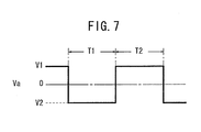
- a drive voltage Va is applied between the upper electrode 14 and the lower electrode 16.
- the drive voltage Va is defined as a voltage, such as a pulse voltage or an alternating-current voltage, which abruptly changes, with time, from a voltage level higher or lower than a reference voltage (e.g., 0 V) to a voltage level that is lower or higher than the reference voltage.
- a reference voltage e.g. 0 V
- a triple junction is formed in a region of contact between the upper surface of the emitter section 12, the upper electrode 14, and a medium (e.g., a vacuum) around the electron emitter 10A.
- the triple junction is defined as an electric field concentration region formed by a contact between the upper electrode 14, the emitter section 12, and the vacuum.
- the triple junction includes a triple point where the upper electrode 14, the emitter section 12, and the vacuum exist as one point.
- the vacuum level in the atmosphere should preferably in the range from 10 2 to 10 -6 Pa and more preferably in the range from 10 -3 to 10 -5 Pa.
- the triple junction is formed on the overhanging portion 26 of the upper electrode 14 and the peripheral area of the upper electrode 14. Therefore, when the drive voltage Va is applied between the upper electrode 14 and the lower electrode 16, an electric field concentration occurs at the triple junction.
- a first electron emission process will first be described below with reference to FIGS. 7 and 8.
- a voltage V2 lower than a reference voltage e.g., 0 V
- a voltage V1 higher than the reference voltage is applied to the lower electrode 16.
- an electric field concentration occurs at the triple junction and/or the tip of the upper electrode 14 to emit electrons from the upper electrode 14 to the emitter section 12, accumulating electrons in the portions of the emitter section 12 which are exposed through the through regions 20 of the upper electrode 14 and regions near the peripheral portion of the upper electrode 14. That is, the electrons are charged in the emitter section 12.
- the upper electrode 14 functions as an electron supply source.
- the voltage level of the drive voltage Va abruptly changes, i.e., the voltage V1 higher than the reference voltage is applied to the upper electrode 14 and the voltage V2 lower than the reference voltage is applied to the lower electrode 16.
- the electrons that have been accumulated in the portions of the emitter 12 which are exposed through the through region 20 of the upper electrode 14 and the regions near the outer peripheral portion of the upper electrode 14 are expelled from the emitter section 12 by dipoles (whose negative poles appear on the surface of the emitter section 12) in the emitter section 12 whose polarization has been reversed in the opposite direction.
- the electrons are emitted from the portions of the emitter section 12 where the electrons have been accumulated, through the through regions 20.
- the electrons are also emitted from the regions near the outer peripheral portion of the upper electrode 14.
- a voltage V3 higher than a reference voltage is applied to the upper electrode 14, and a voltage V4 lower than the reference voltage is applied to the lower electrode 16.
- the electron emitter is prepared for electron emission (e.g., the emitter section 12 is polarized in one direction).
- the voltage level of a drive voltage Va is quickly changed, i.e., the voltage V4 lower than the reference voltage is applied to the upper electrode 14, and the voltage V3 higher than the reference voltage is applied to the lower electrode 16.
- an electric field concentration occurs at the triple junction referred to above, causing the upper electrode 14 to emit primary electrons, which impinge upon the portions of the emitter section 12 which are exposed through the through region 20 and the regions near the outer peripheral portion of the upper electrode 14.
- secondary electrons including reflected primary electrons
- secondary electrons are emitted from the portions hit by the primary electrons.
- secondary electrons are emitted from the through region 20 and the regions near the outer peripheral portion of the upper electrode 14 in an initial stage of the second output period T2.
- the upper electrode 14 since the upper electrode 14 has the through regions 20, electrons are uniformly emitted from each of the through regions 20 and the outer peripheral portions of the upper electrode 14. Thus, variations in the overall electron emission characteristics of the electron emitter section 12 are reduced, making it possible to facilitate the control of the electron emission and increase the electron emission efficiency.
- the gap 28 is formed between the overhanging portion 26 of the upper electrode 14 and the emitter section 12, when the drive voltage Va is applied, an electric field concentration tends to be produced in the region of the gap 28. This leads to a higher efficiency of the electron emission, making the drive voltage lower (emitting electrons at a lower voltage level).
- the upper electrode 12 since the upper electrode 12 has the overhanging portion 26 on the peripheral portion of the through region 20, together with the increased electric field concentration in the region of the gap 28, electrons are easily emitted from the overhanging portion 26 of the upper electrode 14. This leads to a larger output and higher efficiency of the electron emission, making the drive voltage Va lower.
- high luminance is achieved in a display, a light source or the like including an array made up of a lot of the electron emitters 10A.
- the overhanging portion 16 of the upper electrode 14 functions as a gate electrode (a control electrode, a focusing electronic lens, or the like), the straightness of emitted electrons can be increased. This is effective in reducing crosstalk in an electron source of a display using the electron emitters 10A.
- the electron emitter 10A according to the first embodiment is capable of easily developing a high electric field concentration, provides many electron emission regions, has a larger output and higher efficiency of the electron emission, and can be driven at a lower voltage (lower power consumption).
- the upper surface of the emitter section 12 has the surface irregularities 22 due to the grain boundary of the dielectric material.
- the upper electrode 12 has the through regions 20 in portions corresponding to the concavities 24 of the grain boundary of the dielectric material, the overhanging portions 26 of the upper electrode 14 can easily be realized.
- the maximum angle ⁇ between the upper surface of the emitter section 12, i.e., the surface of the convexity 30 (which is also the inner wall surface of the concavity 24) of the grain boundary of the dielectric material, and the lower surface 26a of the overhanging portion 26 of the upper electrode 14 is in the range of 1° ⁇ ⁇ ⁇ 60°.
- the maximum distance d in the vertical direction between the surface of the convexity 30 (the inner wall surface of the concavity 24) of the grain boundary of the dielectric material and the lower surface 26a of the overhanging portion 26 of the upper electrode 14 is in the range of 0 ⁇ m ⁇ d ⁇ 10 ⁇ m.
- the through region 20 is in the shape of the hole 32.
- the portions of the emitter section 12 where the polarization is reversed or changed depending on the drive voltage Va applied between the upper electrode 14 and the lower electrode 16 include a portion (first portion) 40 directly below the upper electrode 14 and a portion (second portion) 42 corresponding to a region extending from the inner peripheral edge of the through region 20 inwardly of the through region 20.
- the second portion 42 changes depending on the level of the drive voltage Va and the degree of the electric field concentration.
- the average diameter of the hole 32 is in the range from 0.1 ⁇ m to 10 ⁇ m. Insofar as the average diameter of the hole 32 is in this range, the distribution of electrons emitted through the through region 20 is almost free of any variations, allowing electrons to be emitted efficiently.
- the average diameter of the hole 32 is less than 0.1 ⁇ m, then the region where electrons are accumulated is made narrower, reducing the amount of emitted electrons. While one solution would be to form many holes 32, it would be difficult and highly costly to form many holes 32. If the average diameter of the hole 32 is in excess of 10 ⁇ m, then the proportion (share) of the portion (second portion) 42 which contributes to the emission of electrons in the portion of the emitter section 12 that is exposed through the through region 20 is reduced, resulting in a reduction in the electron emission efficiency.
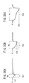
- the overhanging portion 26 of the upper electrode 14 may have upper and lower surfaces extending horizontally as shown in FIG. 3.
- the overhanging portion 26 may have a lower surface 26a extending substantially horizontally and an upper end raised upwardly.
- the overhanging portion 26 may have a lower surface 26a inclined progressively upwardly toward the center of the through region 20.
- the overhanging portion 26 may have a lower surface 26a inclined progressively downwardly toward the center of the through region 20.
- the arrangement shown in FIG. 11 is capable of increasing the function as a gate electrode.
- the arrangement shown in FIG. 13 makes it easier to produce a higher electric field concentration for a larger output and higher efficiency of the electron emission because the gap 28 is narrower.
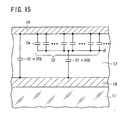
- the electron emitter has in its electrical operation a capacitor C1 due to the emitter section 12 and a cluster of capacitors Ca due to respective gaps 28, disposed between the upper electrode 14 and the lower electrode 16.
- the capacitors Ca due to the respective gaps 28 are connected parallel to each other into a single capacitor C2.
- the capacitor C1 due to the emitter section 12 is connected in series to the capacitor C2 which comprises the cluster of capacitors Ca.
- the capacitor C1 due to the emitter section 12 is not directly connected in series to the capacitor C2 which comprises the cluster of capacitors Ca, but the capacitive component that is connected in series varies depending on the number of the through regions 20 formed in the upper electrode 14 and the overall area of the through regions 20.
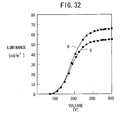
- the capacitor C2 which comprises the cluster of capacitors Ca has a capacitance of 0.885 pF, and the capacitor C1 due to the emitter section 12 has a capacitance of 35.4 pF. If the portion of the capacitor C1 due to the emitter section 12 which is connected in series to the capacitor C2 which comprises the cluster of capacitors Ca is 25 % of the entire capacitor C1, then that series-connected portion has a capacitance (including the capacitance of capacitor C2 which comprises the cluster of capacitors Ca) of 0.805 pF, and the remaining portion has a capacitance of 26.6 pF.
- the overall capacitance is 27.5 pF. This capacitance is 78 % of the capacitance 35.4 pF of the capacitor C1 due to the emitter section 12. Therefore, the overall capacitance is smaller than the capacitance of the capacitor C1 due to the emitter section 12.
- the capacitance of the cluster of capacitors Ca due to the gaps 28 is relatively small. Because of the voltage division between the cluster of capacitors Ca and the capacitor C1 due to the emitter section 12, almost the entire voltage Va is applied across the gaps 28, which are effective to produce a larger output of the electron emission.
- the capacitor C2 which comprises the cluster of capacitors Ca is connected in series to the capacitor C1 due to the emitter section 12, the overall capacitance is smaller than the capacitance of the capacitor C1 due to the emitter section 12. This is effective to provide such preferred characteristics that the electron emission is performed for a larger output and the overall power consumption is lower.
- the glass substrate 11 since the glass substrate 11 is employed, it is possible to produce a large panel, and reduce the production cost. Further, it is possible to lower the process temperature for producing the electron emitter 10A, and lower the cost for facilities. Crystallized glass may be used for the glass substrate 11. In this case, unlike the normal glass, since the process temperature is in a range from 600 to 800°c, selection of the material can be carried out freely.
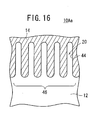
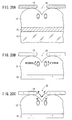
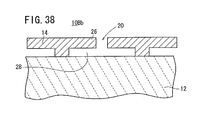
- an electron emitter 10Aa differs from the above electron emitter 10A in that the through region 20 has a shape, particularly a shape viewed from above, in the form of a recess 44.
- the recess 44 should preferably be shaped such that a number of recesses 44 are successively formed into a comb-toothed recess 46.
- the comb-toothed recess 46 is effective to reduce variations in the distribution of electrons emitted through the through region 20 for efficient electron emission.
- the average width represents the average of the lengths of a plurality of different line segments extending perpendicularly across the central line of the recess 44.
- an electron emitter 10Ab according to a second modification differs from the above electron emitter 10A in that the through region 20 has a shape, particularly a shape viewed from above, in the form of a slit 48.
- the slit 48 is defined as something having a major axis (extending in a longitudinal direction) whose length is 10 times or more the length of the minor axis (extending in a transverse direction) thereof. Those having a major axis (extending in a longitudinal direction) whose length is less than 10 times the length of the minor axis (extending in a transverse direction) thereof are defined as holes 32 (see FIG. 4).
- the slit 48 includes a succession of holes 32 in communication with each other.
- the slit 48 should preferably have an average width ranging from 0.1 ⁇ m to 10 ⁇ m for reducing variations in the distribution of electrons emitted through the through region 20 for efficient electron emission.
- the average width represents the average of the lengths of a plurality of different line segments extending perpendicularly across the central line of the slit 48.
- an electron emitter 10Ac differs from the above electron emitter 10A in that a floating electrode 50 exists on the portion of the upper surface of the emitter section 12 which corresponds to the through region 20, e.g., in the concavity 24 due to the grain boundary of the dielectric material.
- the floating electrode 50 also serves as an electron supply source, a number of electrons can be emitted out through the through region 20 in the electron emission stage (second stage).
- the electron emission from the floating electrode 50 may be attributed to an electric field concentration at the triple junction of the floating electrode 50, the dielectric material, and the vacuum.
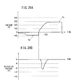
- the characteristics of the electron emitter 10A according to the first embodiment particularly, the voltage vs. charge quantity characteristics (voltage vs. polarized quantity characteristics), will be described below.
- the voltage vs. charge quantity characteristics will be described below. If a region from which electrons are emitted is defined as an electron emission region, then at a point p1 (initial state) where the reference voltage is applied, almost no electrons are stored in the electron emission region. Thereafter, when a negative voltage is applied, the amount of positive charges of dipoles whose polarization is reversed in the emitter section 12 in the electron emission region increases, and electrons are emitted from the upper electrode 14 toward the electron emission region in the first stage, so that electrons are stored.
- the amount of negative charges is the sum of the amount of electrons remaining to be stored and the amount of negative charges of the dipoles whose polarization is reversed in the emitter section 12.
- FIG. 19 The characteristics shown in FIG. 19 will be described below in terms of the voltage vs. charge quantity characteristics.
- the emitter section 12 is polarized in one direction, with dipoles having negative poles facing toward the upper surface of the emitter section 12 in the initial state (see FIG. 20A).
- an electric field concentration occurs at the triple junction and/or the tip of the upper electrode 14, and electrons are emitted from the upper electrode 14 to the emitter section 12 in the first stage, causing electrons to be accumulated in the portion of the emitter section 12 which is exposed through the through region 20 of the upper electrode 14 and the portion of the emitter section 12 which is near the peripheral portion of the upper electrode 14 (see FIG. 20C).
- electrons are emitted (emitted inwardly) from the upper electrode 14 toward the portion of the emitter section 12 which is exposed through the through region 20 of the upper electrode 14.
- the accumulation of electrons is saturated.
- the upper surface of the emitter section 12 is kept charged up to a certain voltage level (see FIG. 21A).
- the level of the positive voltage is increased, there is produced a region where the negative poles of dipole moments start facing the upper surface of the emitter section 12 (see FIG. 21B) immediately prior to the point p4 in FIG. 19.
- the level is further increased, electrons start being emitted due to coulomb repulsive forces posed by the negative poles of the dipoles after the point p4 in FIG. 19 (see FIG. 21C).
- the positive voltage is increased in the positive direction, the amount of emitted electrons is increased.
- the characteristics of the electron emitter 10A have the following features:
- the electron emitter 10A according to the first embodiment has the above characteristics, it can easily be applied to a light source for emitting light from phosphors or a display for displaying an image by emitting electrons from a plurality of electron emitters 10A arrayed in association with respective pixels.
- a display or a light source (hereinafter referred to as the display 100) using the electron emitters 10A according to the first embodiment will be described below.
- an element of the display will be referred to as the "pixel”
- an element of the light source will be referred as the "light-emission element”.
- the display 100 has an electron emission device (light-emission display unit) 102 according to the embodiment of the present invention.
- the light-emission display unit 102 includes a matrix or staggered pattern made up of a large number of electron emitters 10A corresponding to respective pixels, and a drive circuit 104 for driving the light-emission display unit 102.
- One electron emitter 10A may be assigned to each pixel (light-emission element), or a plurality of electron emitters 10A may be assigned to each pixel (light-emission element). In the present embodiment, it is assumed for the sake of brevity that one electron emitter 10A is assigned to each pixel (light-emission element).
- the drive circuit 104 has a plurality of row select lines 106 for selecting rows in the light-emission display unit 102 and a plurality of signal lines 108 for supplying data signals Sd to the light-emission display unit 102.
- the drive circuit 104 also has a row selecting circuit 110 for supplying a selection signal Ss selectively to the row select lines 106 to successively select a row of electron emitters 10A, a signal supplying circuit 112 for outputting parallel data signals Sd to the signal lines 108 to supply the data signals Sd to a row (selected row) selected by the row selecting circuit 110, and a signal control circuit 114 for controlling the row selecting circuit 110 and the signal supplying circuit 112 based on a video signal Sv and a synchronizing signal Sc that are input to the signal control circuit 114.
- a power supply circuit 116 (which supplies 50 V and 0 V, for example) is connected to the row selecting circuit 110 and the signal supplying circuit 112.
- a pulse power supply 118 is connected between a negative line between the row selecting circuit 110 and the power supply circuit 116, and GND (ground).
- the pulse power supply 118 outputs a pulsed voltage waveform having a reference voltage (e.g., 0 V) during a charge accumulation period Td, to be described later, and a certain voltage (e.g., - 400 V) during a light emission period Th.
- the row selecting circuit 110 outputs the selection signal Ss to the selected row and outputs a non-selection signal Sn to the unselected rows.
- the row selecting circuit 110 outputs a constant voltage (e.g., - 350 V) which is the sum of a power supply voltage (e.g., 50 V) from the power supply circuit 116 and a voltage (e.g., - 400 V) from the pulse power supply 118.
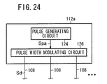
- the signal supplying circuit 112 has a pulse generating circuit 120 and an amplitude modulating circuit 122.
- the pulse generating circuit 120 generates a pulse signal Sp having a constant pulse period and a constant amplitude (e.g., 50 V) during the charge accumulation period Td, and outputs a reference voltage (e.g., 0 V) during the light emission period Th.
- the amplitude modulating circuit 122 amplitude-modulates the pulse signal Sp from the pulse generating circuit 120 depending on the luminance levels of the pixels (light-emission elements) of the selected row, and outputs the amplitude-modulated pulse signal Sp as the data signal Sd for the pixels (light-emission elements) of the selected row.
- the amplitude modulating circuit 122 outputs the reference voltage from the pulse generating circuit 120 as it is.
- the timing control in the amplitude modulating circuit 122 and the supply of the luminance levels of the selected pixels (light-emission elements) to the amplitude modulating circuit 122 are performed by the signal control circuit 114.
- the amplitude of the pulse signal Sp is set to a low level Vsl (see FIG. 23A)
- the amplitude of the pulse signal Sp is set to a medium level Vsm (see FIG. 23B)
- the amplitude of the pulse signal Sp is set to a high level Vsh (see FIG. 23C).
- the amplitude of the pulse signal Sp is modulated into three levels in the above examples, if the amplitude modulation is applied to the display 100, then the pulse signal Sp is amplitude-modulated to 128 levels or 256 levels depending on the luminance levels of the pixels (light-emission elements).
- a modified signal supplying circuit 112a has a pulse generating circuit 124 and a pulse width modulating circuit 126.
- the pulse generating circuit 124 generates and outputs a pulse signal Spa (indicated by the broken lines in FIGS. 25A through 25C) where the positive-going edge of a voltage waveform (indicated by the solid lines in FIGS. 25A through 25C) applied to the electron emitter 10A is continuously changed in level, during the charge accumulation period Td.
- the pulse generating circuit 124 outputs a reference voltage during the light emission period Th.
- the pulse width modulating circuit 126 modulates the pulse width Wp (see FIGS.
- the pulse width modulating circuit 126 outputs the reference voltage from the pulse generating circuit 124 as it is.
- the timing control in the pulse width modulating circuit 126 and the supply of the luminance levels of the selected pixels (light-emission elements) to the pulse with modulating circuit 126 are also performed by the signal control circuit 114.
- the pulse width p of the pulse signal Spa is set to a short width, setting the substantial amplitude to a low level Vsl (see FIG. 25A), if the luminance level is medium, then the pulse width Wp of the pulse signal Spa is set to a medium width, setting the substantial amplitude to a medium level Vsm (see FIG. 25B), and if the luminance level is high, then the pulse width Wp of the pulse signal Spa is set to a long width, setting the substantial amplitude to a high level Vsh (see FIG. 25C).
- the pulse width Wp of the pulse signal Spa is modulated into three levels in the above examples, if the amplitude modulation is applied to the display 100, then the pulse signal Spa is pulse-width-modulated to 128 levels or 256 levels depending on the luminance levels of the pixels (light-emission elements).
- the voltage level at the point p4 where electrons start being emitted is substantially the same. That is, even if the applied voltage changes to the voltage level indicated at the point p4 after electrons are accumulated, the amount of accumulated electrons does not change essentially. It can thus be seen that a memory effect has been produced.
- a transparent plate 130 made of glass or acrylic resin is placed above the upper electrode 14, and a collector electrode 132 in the form of a transparent electrode, for example, is placed on the reverse side of the transparent plate 130 (which faces the upper electrode 14.
- the collector electrode 132 is coated with a phosphor 134.
- a bias voltage source 136 (collector voltage Vc) is connected to the collector electrode 32 through a resistor.
- the electron emitter 10A is placed in a vacuum.
- the vacuum level in the atmosphere should preferably in the range from 10 2 to 10 -6 Pa and more preferably in the range from 10 -3 to 10 -5 Pa.
- the collector electrode 132 functions as a metal back. Electrons emitted from the emitter section 12 pass through the collector electrode 132 into the phosphor 134, exciting the phosphor 134. Therefore, the collector electrode 132 is of a thickness which allows electrons to pass therethrough, preferably be 100 nm or less thick. As the kinetic energy of the emitted electrons is larger, the thickness of the collector electrode 132 may be increased.
- the emission of electrons from the electron emitter 10A was observed. Specifically, as shown in FIG. 29A, a write pulse Pw having a voltage of - 70 V was applied to the electron emitter 10A to cause the electron emitter 10A to accumulate electrons, and thereafter a turn-on pulse Ph having a voltage of 280 V was applied to cause the electron emitter 10A to emit electrons.
- the emission of electrons was measured by detecting the light emission from the phosphor 134 with a light-detecting device (photodiode). The detected waveform is shown in FIG. 29B.
- the write pulse Pw and the turn-on pulse Ph had a duty cycle of 50 %.
- the solid-line curve A represents the characteristics at the time the turn-on pulse Ph had an amplitude of 200 V and the write pulse Pw had an amplitude changing from - 10 V to - 80 V
- the solid-line curve B represents the characteristics at the time the turn-on pulse Ph had an amplitude of 350 V and the write pulse Pw had an amplitude changing from - 10 V to - 80 V.
- the write pulse Pw when the write pulse Pw is changed from - 20 V to - 40 V, it can be understood that the light emission luminance changes substantially linearly.
- a comparison between the amplitudes 350 V and 200 V of the turn-on pulse Ph in particular indicates that a change in the light emission luminance in response to the write pulse Pw at the time the amplitude of the turn-on pulse Ph is 350 V has a wider dynamic range, which is advantageous for increased luminance and contrast for the display of images. This tendency appears to be more advantageous as the amplitude of the turn-on pulse Ph increases in a range until the light emission luminance is saturated with respect to the setting of the amplitude of the turn-on pulse Ph. It is preferable to set the amplitude of the turn-on pulse Ph to an optimum value in relation to the withstand voltage and power consumption of the signal transmission system.
- the solid-line curve C represents the characteristics at the time the write pulse Pw had an amplitude of - 40 V and the turn-on pulse Ph had an amplitude changing from 50 V to 400 V
- the solid-line curve D represents the characteristics at the time the write pulse Pw had an amplitude of - 70 V and the turn-on pulse Ph had an amplitude changing from 50 V to 400 V.
- the solid-line curve E represents the characteristics at the time the level of the collector voltage Vc was 3 kV and the amplitude of the turn-on pulse Ph was changed from 80 V to 500 V
- the solid-line curve F represents the characteristics at the time the level of the collector voltage Vc was 7 kV and the amplitude of the turn-on pulse Ph was changed from 80 V to 500 V.
- a change in the light emission luminance in response to the turn-on pulse Ph has a wider dynamic range when the collector voltage Vc is 7 kV than when the collector voltage Vc is 3 kV, which is advantageous for increased luminance and contrast for the display of images. This tendency appears to be more advantageous as the level of the collector voltage Vc increases. It is preferable also in this case to set the level of the collector voltage Vc to an optimum value in relation to the withstand voltage and power consumption of the signal transmission system.
- a constant voltage is applied to all the electron emitters 10A to cause the electron emitters 10A which correspond to the pixels (light-emission elements) to be turned on to emit electrons in amounts depending on the luminance levels of the corresponding pixels (light-emission elements), thereby emitting light from the pixels (light-emission elements) to be turned on.
- a data signal Sd supplied to the electron emitters 10A which correspond to pixels (light-emission elements) to be turned off (to extinguish light) has a voltage of 50 V, for example. Therefore, a voltage of 0 V is applied to the electron emitters 10A which correspond to pixels (light-emission elements) to be turned off, bringing those electron emitters 10A into a state at the point p1 shown in FIG. 19, so that no electrons are accumulated in those electron emitters 10A.
- a selection signal Ss of 50 V is supplied to the row selection line 106 of the nth row, and a non-selection signal Sn of 0 V is supplied to the row selection lines 106 of the other rows.
- a voltage ranging from -50 V to - 20 V depending on the luminance level is also applied between the upper and lower electrodes 14, 16 of the electron emitter 10A which corresponds to each of the pixels (light-emission elements) to be turned on.
- a voltage ranging from 0 V to 50 V is applied between the upper and lower electrodes 14, 16 of the electron emitter 10A which corresponds to each of unselected pixels (light-emission elements) in the first through (n-1)th rows.
- no electrons are emitted from the electron emitters 10A which correspond to the pixels (light-emission elements) to be turned on, of those unselected pixels (light-emission elements).
- Electrons are thus emitted from the electron emitters 10A which correspond to the pixels (light-emission elements) to be turned on, and the emitted electrons are led to the collector electrodes 132 which correspond to those electron emitters 10A, exciting the corresponding phosphors 134 which emit light. In this manner, an image is displayed on the surface of the transparent plate 130.
- electrons are accumulated in the electron emitters 10A which correspond to the pixels (light-emission elements) to be turned on (to emit light) in the charge accumulation period Td, and the accumulated electrons are emitted for fluorescent light emission in the light emission period Th, for thereby displaying a moving image or a still image on the surface of the transparent plate 130.
- the electron emitter according to the first embodiment can easily be applied to the display 100 which has a plurality of electron emitters 10A arrayed in association with respective pixels (light-emission elements) for emitting electrons from the electron emitters 10A to display an image.
- all the electron emitters 10A are scanned, and voltages depending on the luminance levels of corresponding pixels (light-emission elements) are applied to a plurality of electron emitters 10A which correspond to pixels (light-emission elements) to be turned on, thereby accumulating charges in amounts depending on the luminance levels of the corresponding pixels (light-emission elements) in the electron emitters 10A which correspond to the pixels (light-emission elements) to be turned on.
- a constant voltage is applied to all the electron emitters 10A to cause the electron emitters 10A which correspond to the pixels (light-emission elements) to be turned on to emit electrons in amounts depending on the luminance levels of the corresponding pixels, thereby emitting light from the pixels (light-emission elements) to be turned on.
- the voltage V3 at which the accumulation of electrons is saturated and the voltage V4 at which electrons start being emitted are related to each other by 1 ⁇
- the electron emitters 10A are arranged in a matrix and selected row by row in synchronism with the horizontal scanning period, and data signals Sd depending on the luminance levels of pixels (light-emission elements) are supplied to the selected electron emitters 10A, the data signals Sd are also supplied to unselected pixels (light-emission elements).
- the unselected electron emitters 10A are affected by the data signals Sd and emit electrons, then problems arise in that the quality of displayed images is degraded and the contrast thereof is lowered.
- the electron emitter 10A has the above characteristics. Therefore, even if a simple voltage relationship is employed such that the voltage level of the data signal Sd supplied to the selected electron emitters 10A is set to an arbitrary level from the reference voltage to the voltage V3, and a signal which is opposite in polarity to the data signal Sd, for example, is supplied to the unselected electron emitters 10A, the unselected pixels (light-emission elements) are not affected by the data signal Sd supplied to the selected pixels (light-emission elements). That is, the amount of electrons accumulated by each electron emitter 10A (the amount of charges in the emitter 12 of each electron emitter 10A) in the selection period Ts is maintained until electrons are emitted in the next light emission period Th. As a result, a memory effect is realized in each pixel (light-emission element) for higher luminance and higher contrast.
- a voltage is applied to all the electron emitters 10A, emitting light from the pixels (light-emission elements) which correspond to the electron emitters 10A to be turned on.
- the period Th during which a voltage (emission voltage) for emitting electrons is applied to all the electron emitters 10A is necessarily shorter than one frame.
- the period during which to apply the emission voltage can be reduced, the power consumption can be made much smaller than if charges are accumulated and light is emitted when the pixels (light-emission elements) are scanned.
- the present drive method furthermore, electrons are emitted in the second stage from all the pixels (light-emission elements), independent of the row scanning, separately from the first stage based on the row scanning. Consequently, the light emission time can easily be maintained for increased luminance irrespective of the resolution and the screen size. Since electrons are emitted from all the pixels (light-emission elements) to display as video image, no false contour or image blur occurs in the moving image.
- An electron emitter 10B according to a second embodiment will be described below with reference to FIG. 36.
- the electron emitter 10B according to the second embodiment is of an arrangement that is essentially the same as the electron emitter 10A according to the first embodiment, but is characterized in that the upper electrode 14 and the lower electrode 16 are made of the same material, the upper electrode 14 has a thickness t greater than 10 ⁇ m, and the through region 20 is artificially formed by etching (wet etching or dry etching), liftoff, laser, etc.
- the through region 20 may be shaped as the hole 32, the recess 44, or the slit 48 as with the first embodiment.
- the lower surface 26a of the peripheral portion 26 of the through region 20 in the upper electrode 14 is inclined progressively upwardly toward the center of the through region 20.
- This shape may simply be formed by liftoff, for example.
- floating electrodes 50 may be present on a region of the upper surface of the emitter section 12 which corresponds to the through region 20.
- an electrode having a substantially T-shaped cross-sectional shape may be formed as the upper electrode 14.
- the upper electrode 14, particularly, the peripheral portion 26 of the through region 20 of the upper electrode 14, may be raised.
- This configuration may be achieved by including a material which will be gasified in the sintering process in the film material of the upper electrode 14. In the sintering process, the material is gasified, forming a number of through regions 20 in the upper electrode 14 with the peripheral portions 26 of the through regions 20 being raised.
Landscapes
- Engineering & Computer Science (AREA)
- Chemical & Material Sciences (AREA)
- Nanotechnology (AREA)
- Physics & Mathematics (AREA)
- Mathematical Physics (AREA)
- Theoretical Computer Science (AREA)
- Crystallography & Structural Chemistry (AREA)
- Cathode-Ray Tubes And Fluorescent Screens For Display (AREA)
- Cold Cathode And The Manufacture (AREA)
- Electrodes For Cathode-Ray Tubes (AREA)
- Discharge Lamps And Accessories Thereof (AREA)
Applications Claiming Priority (6)
| Application Number | Priority Date | Filing Date | Title |
|---|---|---|---|
| JP2003345992 | 2003-10-03 | ||
| JP2003345992 | 2003-10-03 | ||
| US730754 | 2003-12-08 | ||
| US10/730,754 US7176609B2 (en) | 2003-10-03 | 2003-12-08 | High emission low voltage electron emitter |
| JP2004187625 | 2004-06-25 | ||
| JP2004187625A JP2005183361A (ja) | 2003-10-03 | 2004-06-25 | 電子放出素子、電子放出装置、ディスプレイ及び光源 |
Publications (1)
| Publication Number | Publication Date |
|---|---|
| EP1521231A2 true EP1521231A2 (de) | 2005-04-06 |
Family
ID=34396858
Family Applications (1)
| Application Number | Title | Priority Date | Filing Date |
|---|---|---|---|
| EP04256108A Withdrawn EP1521231A2 (de) | 2003-10-03 | 2004-10-01 | Elektronen-Emitter, Bildanzeigeeinrichtung mit Elektronenstrahlerzeugungsgerät und Lichtemittierende Vorrichtung |
Country Status (3)
| Country | Link |
|---|---|
| US (1) | US20050073235A1 (de) |
| EP (1) | EP1521231A2 (de) |
| JP (1) | JP2005183361A (de) |
Cited By (1)
| Publication number | Priority date | Publication date | Assignee | Title |
|---|---|---|---|---|
| US7576479B2 (en) | 2006-02-16 | 2009-08-18 | Ngk Insulators, Ltd. | Electron emitter |
Families Citing this family (10)
| Publication number | Priority date | Publication date | Assignee | Title |
|---|---|---|---|---|
| JP4794227B2 (ja) * | 2004-07-15 | 2011-10-19 | 日本碍子株式会社 | 電子放出素子 |
| JP4753561B2 (ja) * | 2004-09-30 | 2011-08-24 | 日本碍子株式会社 | 電子放出装置 |
| JP2007095409A (ja) * | 2005-09-28 | 2007-04-12 | Ngk Insulators Ltd | 電子放出素子、及び電子放出素子の製造方法 |
| JP5024954B2 (ja) * | 2006-01-20 | 2012-09-12 | 日本電気株式会社 | 光学素子、光集積デバイス、および光情報伝搬システム |
| JP2007242375A (ja) * | 2006-03-07 | 2007-09-20 | Ngk Insulators Ltd | 電子放出装置及び同電子放出装置の製造方法 |
| JP5004484B2 (ja) | 2006-03-23 | 2012-08-22 | 日本碍子株式会社 | 誘電体デバイス |
| US7727584B2 (en) | 2007-02-19 | 2010-06-01 | Ngk Insulators, Ltd. | Dielectric device and its manufacturing method |
| US7727585B2 (en) | 2007-02-19 | 2010-06-01 | Ngk Insulators, Ltd. | Dielectric device and its manufacturing method |
| JP5188094B2 (ja) * | 2007-04-20 | 2013-04-24 | キヤノン株式会社 | 駆動装置、露光装置及びデバイス製造方法 |
| JP6461546B2 (ja) * | 2014-10-10 | 2019-01-30 | シャープ株式会社 | 電子放出装置 |
Family Cites Families (36)
| Publication number | Priority date | Publication date | Assignee | Title |
|---|---|---|---|---|
| JP3126158B2 (ja) * | 1991-04-10 | 2001-01-22 | 日本放送協会 | 薄膜冷陰極 |
| US6313815B1 (en) * | 1991-06-06 | 2001-11-06 | Canon Kabushiki Kaisha | Electron source and production thereof and image-forming apparatus and production thereof |
| US5453661A (en) * | 1994-04-15 | 1995-09-26 | Mcnc | Thin film ferroelectric flat panel display devices, and methods for operating and fabricating same |
| US5508590A (en) * | 1994-10-28 | 1996-04-16 | The Regents Of The University Of California | Flat panel ferroelectric electron emission display system |
| US5747926A (en) * | 1995-03-10 | 1998-05-05 | Kabushiki Kaisha Toshiba | Ferroelectric cold cathode |
| US5666019A (en) * | 1995-09-06 | 1997-09-09 | Advanced Vision Technologies, Inc. | High-frequency field-emission device |
| KR100369066B1 (ko) * | 1995-12-29 | 2003-03-28 | 삼성에스디아이 주식회사 | 강유전성에미터를적용한음극구조체및이를적용한전자총과음극선관 |
| US5729094A (en) * | 1996-04-15 | 1998-03-17 | Massachusetts Institute Of Technology | Energetic-electron emitters |
| JP2907113B2 (ja) * | 1996-05-08 | 1999-06-21 | 日本電気株式会社 | 電子ビーム装置 |
| US5726524A (en) * | 1996-05-31 | 1998-03-10 | Minnesota Mining And Manufacturing Company | Field emission device having nanostructured emitters |
| DE19651552A1 (de) * | 1996-12-11 | 1998-06-18 | Patent Treuhand Ges Fuer Elektrische Gluehlampen Mbh | Kaltkathode für Entladungslampen, Entladungslampe mit dieser Kaltkathode und Betriebsweise für diese Entladungslampe |
| JP2950274B2 (ja) * | 1997-01-28 | 1999-09-20 | 日本電気株式会社 | 電界放出型冷陰極素子の駆動方法及び電界放出型冷陰極電子銃 |
| US5990605A (en) * | 1997-03-25 | 1999-11-23 | Pioneer Electronic Corporation | Electron emission device and display device using the same |
| JP3570864B2 (ja) * | 1997-08-08 | 2004-09-29 | パイオニア株式会社 | 電子放出素子及びこれを用いた表示装置 |
| EP0935274B1 (de) * | 1997-08-27 | 2003-10-01 | Matsushita Electric Industrial Co., Ltd. | Elektronen emittierende vorrichtung, feldemissionsanzeigevorrichtung und herstellungsverfahren derselben |
| JPH11213866A (ja) * | 1998-01-22 | 1999-08-06 | Sony Corp | 電子放出装置及びその製造方法並びにこれを用いた表示装置 |
| US6285123B1 (en) * | 1998-09-11 | 2001-09-04 | Pioneer Corporation | Electron emission device with specific island-like regions |
| JP3293571B2 (ja) * | 1998-10-28 | 2002-06-17 | 日本電気株式会社 | 電界放出型冷陰極素子及びその駆動方法並びにそれらを用いた画像表示装置 |
| JP3382172B2 (ja) * | 1999-02-04 | 2003-03-04 | 株式会社日立製作所 | 横型絶縁ゲートバイポーラトランジスタ |
| US6198225B1 (en) * | 1999-06-07 | 2001-03-06 | Symetrix Corporation | Ferroelectric flat panel displays |
| GB9918885D0 (en) * | 1999-08-10 | 1999-10-13 | Pharmacia & Upjohn Spa | Pharmaceutical formulations in hydroxypropymethycellulose capsules |
| US6359383B1 (en) * | 1999-08-19 | 2002-03-19 | Industrial Technology Research Institute | Field emission display device equipped with nanotube emitters and method for fabricating |
| US6479924B1 (en) * | 2000-08-11 | 2002-11-12 | Samsung Electronics Co., Ltd. | Ferroelectric emitter |
| JP3639808B2 (ja) * | 2000-09-01 | 2005-04-20 | キヤノン株式会社 | 電子放出素子及び電子源及び画像形成装置及び電子放出素子の製造方法 |
| JP2002169507A (ja) * | 2000-11-30 | 2002-06-14 | Fujitsu Ltd | プラズマディスプレイパネル及びその駆動方法 |
| EP1265263A4 (de) * | 2000-12-22 | 2006-11-08 | Ngk Insulators Ltd | Elektronenemissionselement und dieses verwen-dende feldemissionsanzeige |
| US6946800B2 (en) * | 2002-02-26 | 2005-09-20 | Ngk Insulators, Ltd. | Electron emitter, method of driving electron emitter, display and method of driving display |
| JP3822551B2 (ja) * | 2002-09-30 | 2006-09-20 | 日本碍子株式会社 | 発光素子及びそれを具えるフィールドエミッションディスプレイ |
| JP2004146364A (ja) * | 2002-09-30 | 2004-05-20 | Ngk Insulators Ltd | 発光素子及びそれを具えるフィールドエミッションディスプレイ |
| JP2004172087A (ja) * | 2002-11-05 | 2004-06-17 | Ngk Insulators Ltd | ディスプレイ |
| US7187114B2 (en) * | 2002-11-29 | 2007-03-06 | Ngk Insulators, Ltd. | Electron emitter comprising emitter section made of dielectric material |
| JP3867065B2 (ja) * | 2002-11-29 | 2007-01-10 | 日本碍子株式会社 | 電子放出素子及び発光素子 |
| US6975074B2 (en) * | 2002-11-29 | 2005-12-13 | Ngk Insulators, Ltd. | Electron emitter comprising emitter section made of dielectric material |
| US7129642B2 (en) * | 2002-11-29 | 2006-10-31 | Ngk Insulators, Ltd. | Electron emitting method of electron emitter |
| US20040256995A1 (en) * | 2003-03-26 | 2004-12-23 | Ngk Insulators, Ltd. | Display and method for driving display |
| US7017628B2 (en) * | 2004-05-25 | 2006-03-28 | California Pacific Lab, Inc. | Ecologically friendly funnel |
-
2004
- 2004-06-25 JP JP2004187625A patent/JP2005183361A/ja not_active Abandoned
- 2004-09-28 US US10/951,509 patent/US20050073235A1/en not_active Abandoned
- 2004-10-01 EP EP04256108A patent/EP1521231A2/de not_active Withdrawn
Cited By (2)
| Publication number | Priority date | Publication date | Assignee | Title |
|---|---|---|---|---|
| US7576479B2 (en) | 2006-02-16 | 2009-08-18 | Ngk Insulators, Ltd. | Electron emitter |
| EP1826798A3 (de) * | 2006-02-16 | 2009-11-11 | Ngk Insulators, Ltd. | Elektronenemitter |
Also Published As
| Publication number | Publication date |
|---|---|
| JP2005183361A (ja) | 2005-07-07 |
| US20050073235A1 (en) | 2005-04-07 |
Similar Documents
| Publication | Publication Date | Title |
|---|---|---|
| US20040100200A1 (en) | Electron emitter, method of driving electron emitter, display and method of driving display | |
| US7230371B2 (en) | Light source | |
| EP1521231A2 (de) | Elektronen-Emitter, Bildanzeigeeinrichtung mit Elektronenstrahlerzeugungsgerät und Lichtemittierende Vorrichtung | |
| EP1523026B1 (de) | Elektronenemitter | |
| US7379037B2 (en) | Display apparatus, method of driving display apparatus, electron emitter, method of driving electron emitter, apparatus for driving electron emitter, electron emission apparatus, and method of driving electron emission apparatus | |
| US20040256995A1 (en) | Display and method for driving display | |
| US7071628B2 (en) | Electronic pulse generation device | |
| EP1463022A2 (de) | Bildanzeigeeinrichtung mit Elektronenstrahlerzeugungsgerät, Verfahren und Steuerungsgerät dieser Bildanzeigeeinrichtung. | |
| US7129642B2 (en) | Electron emitting method of electron emitter | |
| US7336026B2 (en) | High efficiency dielectric electron emitter | |
| US6897620B1 (en) | Electron emitter, drive circuit of electron emitter and method of driving electron emitter | |
| US20050073234A1 (en) | Electron emitter | |
| US7474060B2 (en) | Light source | |
| US20050116603A1 (en) | Electron emitter | |
| JP3867078B2 (ja) | 電子放出素子 | |
| EP1607929A2 (de) | Feldemissionsanzeigevorrichtung | |
| US20060214557A1 (en) | Light source | |
| EP1521232A2 (de) | Elektronen-Emitter, Bildanzeigeeinrichtung mit Elektronenstrahlerzeugungsgerät. | |
| EP1376641A2 (de) | Elektronen-Emitter, Ansteuerkreis für Elektronen-Emitter und Verfahren zur Ansteuerung von Elektronen-Emitter | |
| EP1424716A1 (de) | Verfahren zur Elektronenemission eines Elektronenemitters | |
| US20060214556A1 (en) | Light source | |
| EP1510998A2 (de) | Elektronen-emittierende Vorrichtung, Lichtquelle und Bildanzeigegerät | |
| EP1705689A2 (de) | Lichtquelle | |
| JP4097230B2 (ja) | 電子放出素子 | |
| WO2006070446A1 (ja) | 電子放出素子、電子放出装置、ディスプレイ及び光源 |
Legal Events
| Date | Code | Title | Description |
|---|---|---|---|
| PUAI | Public reference made under article 153(3) epc to a published international application that has entered the european phase |
Free format text: ORIGINAL CODE: 0009012 |
|
| AK | Designated contracting states |
Kind code of ref document: A2 Designated state(s): AT BE BG CH CY CZ DE DK EE ES FI FR GB GR HU IE IT LI LU MC NL PL PT RO SE SI SK TR |
|
| AX | Request for extension of the european patent |
Extension state: AL HR LT LV MK |
|
| STAA | Information on the status of an ep patent application or granted ep patent |
Free format text: STATUS: THE APPLICATION HAS BEEN WITHDRAWN |
|
| 18W | Application withdrawn |
Effective date: 20070315 |