EP1521413A2 - Réception multiporteuse à estimation de canal et égalisation - Google Patents
Réception multiporteuse à estimation de canal et égalisation Download PDFInfo
- Publication number
- EP1521413A2 EP1521413A2 EP04023312A EP04023312A EP1521413A2 EP 1521413 A2 EP1521413 A2 EP 1521413A2 EP 04023312 A EP04023312 A EP 04023312A EP 04023312 A EP04023312 A EP 04023312A EP 1521413 A2 EP1521413 A2 EP 1521413A2
- Authority
- EP
- European Patent Office
- Prior art keywords
- frequency response
- generating
- frequency
- response
- fourier transform
- Prior art date
- Legal status (The legal status is an assumption and is not a legal conclusion. Google has not performed a legal analysis and makes no representation as to the accuracy of the status listed.)
- Withdrawn
Links
Images
Classifications
-
- H—ELECTRICITY
- H04—ELECTRIC COMMUNICATION TECHNIQUE
- H04L—TRANSMISSION OF DIGITAL INFORMATION, e.g. TELEGRAPHIC COMMUNICATION
- H04L25/00—Baseband systems
- H04L25/02—Details ; arrangements for supplying electrical power along data transmission lines
- H04L25/0202—Channel estimation
- H04L25/0224—Channel estimation using sounding signals
- H04L25/0228—Channel estimation using sounding signals with direct estimation from sounding signals
- H04L25/023—Channel estimation using sounding signals with direct estimation from sounding signals with extension to other symbols
- H04L25/0232—Channel estimation using sounding signals with direct estimation from sounding signals with extension to other symbols by interpolation between sounding signals
- H04L25/0234—Channel estimation using sounding signals with direct estimation from sounding signals with extension to other symbols by interpolation between sounding signals by non-linear interpolation
-
- H—ELECTRICITY
- H04—ELECTRIC COMMUNICATION TECHNIQUE
- H04L—TRANSMISSION OF DIGITAL INFORMATION, e.g. TELEGRAPHIC COMMUNICATION
- H04L27/00—Modulated-carrier systems
- H04L27/26—Systems using multi-frequency codes
- H04L27/2601—Multicarrier modulation systems
- H04L27/2647—Arrangements specific to the receiver only
-
- H—ELECTRICITY
- H04—ELECTRIC COMMUNICATION TECHNIQUE
- H04L—TRANSMISSION OF DIGITAL INFORMATION, e.g. TELEGRAPHIC COMMUNICATION
- H04L25/00—Baseband systems
- H04L25/02—Details ; arrangements for supplying electrical power along data transmission lines
- H04L25/03—Shaping networks in transmitter or receiver, e.g. adaptive shaping networks
- H04L25/03006—Arrangements for removing intersymbol interference
- H04L2025/0335—Arrangements for removing intersymbol interference characterised by the type of transmission
- H04L2025/03375—Passband transmission
- H04L2025/03414—Multicarrier
-
- H—ELECTRICITY
- H04—ELECTRIC COMMUNICATION TECHNIQUE
- H04L—TRANSMISSION OF DIGITAL INFORMATION, e.g. TELEGRAPHIC COMMUNICATION
- H04L25/00—Baseband systems
- H04L25/02—Details ; arrangements for supplying electrical power along data transmission lines
- H04L25/03—Shaping networks in transmitter or receiver, e.g. adaptive shaping networks
- H04L25/03006—Arrangements for removing intersymbol interference
- H04L2025/03433—Arrangements for removing intersymbol interference characterised by equaliser structure
- H04L2025/03439—Fixed structures
- H04L2025/03522—Frequency domain
-
- H—ELECTRICITY
- H04—ELECTRIC COMMUNICATION TECHNIQUE
- H04L—TRANSMISSION OF DIGITAL INFORMATION, e.g. TELEGRAPHIC COMMUNICATION
- H04L25/00—Baseband systems
- H04L25/02—Details ; arrangements for supplying electrical power along data transmission lines
- H04L25/0202—Channel estimation
- H04L25/0212—Channel estimation of impulse response
- H04L25/0216—Channel estimation of impulse response with estimation of channel length
-
- H—ELECTRICITY
- H04—ELECTRIC COMMUNICATION TECHNIQUE
- H04L—TRANSMISSION OF DIGITAL INFORMATION, e.g. TELEGRAPHIC COMMUNICATION
- H04L25/00—Baseband systems
- H04L25/02—Details ; arrangements for supplying electrical power along data transmission lines
- H04L25/0202—Channel estimation
- H04L25/0212—Channel estimation of impulse response
- H04L25/0218—Channel estimation of impulse response with detection of nulls
Definitions
- the present invention relates to a receiving apparatus and receiving method for receiving signals transmitted using an OFDM (orthogonal frequency division multiplexing) system.
- OFDM orthogonal frequency division multiplexing
- the OFDM signal transmission system modulates multiple mutually orthogonal carriers with the digital data being transmitted, and then multiplexes these modulated signals before transmission.
- Increasing the number of carriers from several hundred to several thousand for OFDM transmission significantly increases the symbol period compared with a single carrier system at the same transmission rate, and thus lowers the likelihood of multipath interference.
- the amplitude and phase of each carrier changes on the channel, and the receiver must compensate for this change.
- All or part of an OFDM carrier is therefore used to transmit a pilot signal (a signal of known amplitude and phase).
- the receiver can therefore estimate from the received pilot signal how the carrier changed on the channel, or more specifically can estimate the frequency response of the channel, and compensate accordingly.
- the pilot signal used in the DVB-T Digital Video Broadcast - Terrestrial: digital terrestrial television system used in Europe
- ISDB-T Integrated Services Digital Broadcasting - Terrestrial: digital terrestrial television system used in Japan
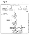
- Fig. 11 is a block diagram of the OFDM signal demodulator 12a taught in U.S. Patent No. 5,307,376 (Japanese Patent No. 3044899).
- the pilot signal extraction circuit 31 extracts the pilot signal contained in the output of the Fourier transform circuit 22, and outputs the result to the first input of a divider 33.
- the pilot signal generator 32 generates a pilot signal of known amplitude and phase synchronized to the pilot signal extraction circuit 31, and outputs the resulting pilot signal to the second input of the divider 33.
- the divider 33 then divides the output of the pilot signal extraction circuit 31 by the output of the pilot signal generator 32 to acquire the frequency response of the channel sampled at the pilot signal interval, and then outputs the result to the zero signal insertion circuit 34a.
- the zero signal insertion circuit 34a inserts a zero signal to the output of the divider 33, and supplies the result to the inverse Fourier transform circuit 35a.
- the inverse Fourier transform circuit 35a converts the frequency response output from the zero signal insertion circuit 34a to an impulse response, and outputs the result to the coring circuit 36a.
- the coring circuit 36a replaces data equal to or less than a specified threshold value in the output of the inverse Fourier transform circuit 35a with a zero signal, and outputs the result to the truncation circuit 37a.
- the truncation circuit 37a truncates the coring circuit output to a specified length and replaces other data with a zero signai to remove aliasing components (due to the frequency response, which is the input to the inverse Fourier transform circuit 35a, being sampled at the pilot signal period).
- the truncation circuit 37a outputs the result to the Fourier transform circuit 38a.
- the Fourier transform circuit 38a generates the interpolated frequency response (having values at positions other than the pilot signal) by Fourier transform of the impulse response output from the truncation circuit 37a.
- the output from the Fourier transform circuit 38a is then supplied as the output of the channel estimation circuit 23a to the second input to the divider 24.
- the DFT block 11 shown in Fig. 1 in the above-noted U.S. Patent No. 5,307,376 corresponds to the Fourier transform circuit 22 shown in Fig. 11; the projection block 12 similarly shown in U.S. Patent No. 5,307,376 corresponds to the divider 24 in Fig. 11; N/R sample extraction circuit 13 similarly shown in U.S. Patent No. 5,307,376 corresponds to the circuit block including the pilot signal generator 32, divider 33, and zero signal insertion circuit 34a in Fig. 11; DFT -1 14 similarly shown in U.S. Patent No. 5,307,376 corresponds to the inverse Fourier transform circuit 35a in Fig. 11; weighting circuit 15 similarly shown in U.S. Patent No.
- 5,307,376 corresponds to the truncation circuit 37a in Fig. 11; DFT 16 similarly shown in U.S. Patent No. 5,307,376 corresponds to the Fourier transform circuit 38a in Fig. 11; and thresholding block 17 similarly shown in U.S. Patent No. 5,307,376 corresponds to the coring circuit 36a in Fig. 11.
- n is an index denoting the sampling time
- N denotes the number of samples processed by the inverse Fourier transform circuit 35a and Fourier transform circuit 38a.
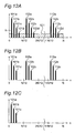
- Fig. 12 (a) shows an example of output from the inverse Fourier transform circuit 35a wherein 101 a to 101 d denote the normal impulse response, 102a to 102d through 112a to 112d denote the aliasing component, and the shaded area indicates the noise component 121. Aliasing occurs every N/12 samples because the scattered pilot signal in the DVB-T and ISDB-T systems is located every 12 carriers in each symbol.
- Fig. 12 (b) shows an example of output from the coring circuit 36a.
- the coring circuit 36a replaces data equal to or less than a specified threshold value (th) with zero signals.
- Data other than 101 a to 101 c, and 102a to 1 02c through 112a to 112c are therefore replaced by zero signals in the example shown in Fig. 12, and the power of noise components is therefore significantly suppressed.
- Fig. 12 (c) shows the output of the truncation circuit 37a. Note that aliasing components 102a to 102c through 112a to 112c are removed because the truncation circuit 37a substitutes zero signals for data with an index greater than N/12.
- the frequency response acquired by the Fourier transform circuit 38a applying Fourier transform to the output of the truncation circuit 37a is thus not only interpolated, but estimation error due to noise is reduced by the operation of the coring circuit 36a.
- output from the inverse Fourier transform circuit 35a has side lobes rather than being a single impulse. Furthermore, impulse response is at the sampling time, output from the inverse Fourier transform circuit 35a also has side lobes rather than being a single impulse because the bandwidth of the output from the zero signal insertion circuit 34a is narrower than the input bandwidth of the inverse Fourier transform circuit 35a.
- the inverse Fourier transform circuit 35a and Fourier transform circuit 38a must also process the same number of data samples as the main Fourier Transform circuit 22, leading to an increased circuit size if this operation is run in dedicated hardware, and an increased processing load if run in software using general-purpose hardware such as a DSP (digital signal processor).
- DSP digital signal processor
- the present invention is directed to solving the foregoing problem, and an object of the invention is to provide an OFDM signal receiving apparatus that reduces frequency response estimation error while also reducing the circuit scale required for a hardware implementation and the processing load required for a software implementation.
- a first aspect of the present invention is a receiving apparatus for receiving OFDM (orthogonal frequency division multiplexing) signals containing a pilot signal of known amplitude and phase, the OFDM signal receiving apparatus including a first Fourier transform means for generating an OFDM signal in the frequency domain by a Fourier transform of the OFDM signal; a first dividing means for dividing the pilot signal contained in the frequency domain OFDM signal by a specified pilot signal, and generating a first frequency response; a zero insertion means for inserting zero signals to the first frequency response, and generating a second frequency response; a window function multiplying means for multiplying the second frequency response by a window function, and generating a third frequency response; an inverse Fourier transform means for generating a first impulse response by an inverse Fourier transform of the third frequency response; a coring means for replacing data in the first impulse response less than or equal to a specified threshold value with zero signals, and generating a second impulse response; a truncation means for trun
- a second aspect of the invention is an OFDM signal receiving apparatus for receiving OFDM signals containing a pilot signal of known amplitude and phase, the OFDM signal receiving apparatus including a first Fourier transform means for generating an OFDM signal in the frequency domain by a Fourier transform of the OFDM signal; a first dividing means for dividing the pilot signal contained in the frequency domain OFDM signal by a specified pilot signal, and generating a first frequency response; a zero insertion means for inserting zero signals to the first frequency response, and generating a second frequency response; an inverse Fourier transform means for generating a first impulse response by an inverse Fourier transform of the second frequency response; a coring means for replacing data in the first impulse response less than or equal to a specified threshold value with zero signals, and generating a second impulse response; a truncation means for truncating the second impulse response at a specified data length, replacing other data with zero signals, and generating a third impulse response; a second Fourier transform means for generating a third frequency response by a
- a third aspect of the invention is an OFDM signal receiving apparatus for receiving OFDM signals containing a pilot signal of known amplitude and phase, the OFDM signal receiving apparatus including a first Fourier transform means for generating an OFDM signal in the frequency domain by a Fourier transform of the OFDM signal; a first dividing means for dividing the pilot signal contained in the frequency domain OFDM signal by a specified pilot signal, and generating a first frequency response; a zero insertion means for inserting zero signals to the first frequency response, and generating a second frequency response; a window function multiplying means for multiplying the second frequency response by a window function, and generating a third frequency response; an inverse Fourier transform means for generating a first impulse response by an inverse Fourier transform of the third frequency response; a coring means for replacing data in the first impulse response less than or equal to a specified threshold value with zero signals, and generating a second impulse response; a truncation means for truncating the second impulse response at a specified data length, replacing other data with zero
- a fourth aspect of the invention is an OFDM signal receiving apparatus as described in aspect 1 or 3 above wherein the window function multiplying means is disposed upstream of the zero insertion means.
- a fifth aspect of the invention is an OFDM signal receiving apparatus for receiving OFDM signals containing a pilot signal of known amplitude and phase, the OFDM signal receiving apparatus including a first Fourier transform means for generating an OFDM signal in the frequency domain by a Fourier transform of the OFDM signal; a first dividing means for dividing the pilot signal contained in the frequency domain OFDM signal by a specified pilot signal, and generating a first frequency response; an inverse Fourier transform means for generating a first impulse response by an inverse Fourier transform of the first frequency response; a coring means for replacing data in the first impulse response less than or equal to a specified threshold value with zero signals, and generating a second impulse response; a second Fourier transform means for generating a second frequency response by a Fourier transform of the second impulse response; a time axis interpolation means for interpolating the second frequency response along the time axis, and generating a third frequency response; a frequency axis interpolation means for interpolating the third frequency response along the frequency axis
- a sixth aspect of the invention is an OFDM signal receiving apparatus for receiving OFDM signals containing a pilot signal of known amplitude and phase, the OFDM signal receiving apparatus including a first Fourier transform means for generating an OFDM signal in the frequency domain by a Fourier transform of the OFDM signal; a first dividing means for dividing the pilot signal contained in the frequency domain OFDM signal by a specified pilot signal, and generating a first frequency response; a window function multiplying means for multiplying the first frequency response by a window function, and generating a second frequency response; an inverse Fourier transform means for generating a first impulse response by an inverse Fourier transform of the second frequency response; a coring means for replacing data in the first impulse response less than or equal to a specified threshold value with zero signals, and generating a second impulse response; a second Fourier transform means for generating a third frequency response by a Fourier transform of the second impulse response; a window function dividing means for dividing the third frequency response by the window function, and generating a fourth frequency response;
- a seventh aspect of the invention is an OFDM signal receiving apparatus for receiving OFDM signals containing a pilot signal of known amplitude and phase, the OFDM signal receiving apparatus including a first Fourier transform means for generating an OFDM signal in the frequency domain by a Fourier transform of the OFDM signal; a first dividing means for dividing the pilot signal contained in the frequency domain OFDM signal by a specified pilot signal, and generating a first frequency response; a coring means for replacing data in the first impulse response less than or equal to a specified threshold value with zero signals, and generating a second impulse response; a second Fourier transform means for generating a second frequency response by a Fourier transform of the second impulse response; a selection means for selecting the second frequency response for carriers within a specific range of the signal band center, selecting the first frequency response for the remaining carriers near the signal band edges, and generating a third frequency response; a time axis interpolation means for interpolating the third frequency response along the time axis, and generating a fourth frequency response; a frequency axi
- An eighth aspect of the invention is an OFDM signal receiving apparatus for receiving OFDM signals containing a pilot signal of known amplitude and phase, the OFDM signal receiving apparatus including a first Fourier transform means for generating an OFDM signal in the frequency domain by a Fourier transform of the OFDM signal; a first dividing means for dividing the pilot signal contained in the frequency domain OFDM signal by a specified pilot signal, and generating a first frequency response; a window function multiplying means for multiplying the first frequency response by a window function, and generating a second frequency response; an inverse Fourier transform means for generating a first impulse response by an inverse Fourier transform of the second frequency response; a coring means for replacing data in the first impulse response less than or equal to a specified threshold value with zero signals, and generating a second impulse response; a second Fourier transform means for generating a third frequency response by a Fourier transform of the second impulse response; a window function dividing means for dividing the third frequency response by the window function, and generating a fourth frequency response;
- a ninth aspect of the invention OFDM signal receiving apparatus as described in the foregoing aspect 5 or 7 wherein the time axis interpolating means is disposed upstream of the inverse Fourier transform means.
- a tenth aspect of the invention is an OFDM signal receiving apparatus as described in the foregoing aspect 6 or 8 wherein the time axis interpolating means is disposed upstream of the window function multiplying means.
- An eleventh aspect of the invention is an OFDM signal receiving apparatus for receiving OFDM signals containing a pilot signal of known amplitude and phase, the OFDM signal receiving apparatus including a first Fourier transform means for generating an OFDM signal in the frequency domain by a Fourier transform of the OFDM signal; a first dividing means for dividing the pilot signal contained in the frequency domain OFDM signal by a specified pilot signal, and generating a first frequency response; a window function multiplying means for multiplying the first frequency response by a window function, and generating a second frequency response; an inverse Fourier transform means for generating a first impulse response by an inverse Fourier transform of the second frequency response; a coring means for replacing data in the first impulse response less than or equal to a specified threshold value with zero signals, and generating a second impulse response; a second Fourier transform means for generating a third frequency response by a Fourier transform of the second impulse response; a window function dividing means for dividing the third frequency response by the window function, and generating a fourth frequency response;
- a twelfth aspect of the invention is an OFDM signal receiving apparatus for receiving OFDM signals containing a pilot signal of known amplitude and phase, the OFDM signal receiving apparatus including a first Fourier transform means for generating an OFDM signal in the frequency domain by a Fourier transform of the OFDM signal; a first dividing means for dividing the pilot signal contained in the frequency domain OFDM signal by a specified pilot signal, and generating a first frequency response; a coring means for replacing data in the first impulse response less than or equal to a specified threshold value with zero signals, and generating a second impulse response; a second Fourier transform means for generating a second frequency response by a Fourier transform of the second impulse response; a selection means for selecting the second frequency response for carriers within a specific range of the signal band center, selecting the first frequency response for the remaining carriers near the signal band edges, and generating a third frequency response; a holding means for holding the third frequency response for a specific time, and generating a fourth frequency response; and a second dividing means for dividing
- a thirteenth aspect of the invention is an OFDM signal receiving apparatus for receiving OFDM signals containing a pilot signal of known amplitude and phase, the OFDM signal receiving apparatus including a first Fourier transform means for generating an OFDM signal in the frequency domain by a Fourier transform of the OFDM signal; a first dividing means for dividing the pilot signal contained in the frequency domain OFDM signal by a specified pilot signal, and generating a first frequency response; a window function multiplying means for multiplying the first frequency response by a window function, and generating a second frequency response; an inverse Fourier transform means for generating a first impulse response by an inverse Fourier transform of the second frequency response; a coring means for replacing data in the first impulse response less than or equal to a specified threshold value with zero signals, and generating a second impulse response; a second Fourier transform means for generating a third frequency response by a Fourier transform of the second impulse response; a window function dividing means for dividing the third frequency response by the window function, and generating a fourth frequency response;
- a fourteenth aspect of the invention is an OFDM signal receiving apparatus as described in any one of aspects 11 to 13 wherein the OFDM signal has a finite length frame structure including a pilot symbol of known amplitude and phase for all carriers as the preamble; and the holding means holds the frequency response to the end of the frame.
- a fifteenth aspect of the invention is an OFDM signal receiving apparatus as described in any one of aspects 11 to 13 wherein the OFDM signal has a continuous frame structure with a pilot symbol of known amplitude and phase for all carriers inserted each frame period; and the holding means holds the frequency response for the frame period.
- a sixteenth aspect of the invention is an OFDM signal receiving apparatus as described in any one of aspects 1 to 15 wherein the threshold value used by the coring means is constant.
- a seventeenth aspect of the invention is an OFDM signal receiving apparatus as described in any one of aspects 1 to 15 wherein the threshold value used by the coring means is appropriately controlled.
- An eighteenth aspect of the invention is an OFDM signal receiving apparatus as described in aspect 17 wherein the threshold value used by the coring means is controlled according to the impulse response.
- a nineteenth aspect of the invention is an OFDM signal receiving apparatus as described in aspect 17 wherein the threshold value used by the coring means is controlled according to the noise level.
- a twentieth aspect of the invention is an OFDM signal receiving apparatus as described in aspect 1, 3, 6, 8, 11, or 13 wherein the window function is a Hamming window, Hanning window, or Blackman window.
- An OFDM signal receiving apparatus improves reception performance by reducing frequency response estimation error, and reduces the circuit scale required for a hardware implementation and the processing load required for a software implementation.
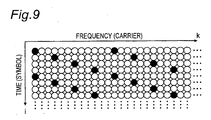
- Fig. 9 shows an example of a signal received by the OFDM signal receiver of the present invention, and schematically shows pilot signal arrangement in the DVB-T and ISDB-T systems.
- k on the x-axis is the carrier index
- i on the y-axis is the symbol index.
- Solid dots represent the scattered pilot
- open circles represent the data carrier containing control information (TPS (transmission parameter signalling) in DVB-T
- TMCC transmission multiplexing configuration control
- AC auxiliary channel
- the scattered pilot is inserted at every 12th carrier in each symbol with the location shifted three carriers in each symbol.
- the scattered pilot is also modulated using a pseudo random binary sequence; the amplitude and phase are determined only by the carrier index k, and are independent of the symbol index i.
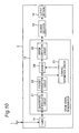
- Fig. 10 is a block diagram of an OFDM signal receiving apparatus according to the present invention.
- a signal received by the antenna 1 is supplied to the tuner 11 in the OFDM signal receiver 2.
- the tuner 11 extracts the OFDM signal containing the desired service from the reception signal supplied from the antenna, frequency converts the signal from the RF (radio frequency) band to the IF (intermediate frequency) band, and adjusts the gain, and then supplies the resulting output to an OFDM signal demodulator 12.
- the OFDM signal demodulator 12 demodulates the tuner 11 output to restore the transmitted digital data, applies an error correction and decoding process to correct transmission error caused by noise, for example, added to the signal on the channel, and then supplies the resulting output to the source decoder 13.
- the source decoder 13 separates the output from the OFDM signal demodulator 12 into video and audio data, applies a data decompression process, and supplies the resulting output to the output section 14.
- the output section 14 then provides the desired service to the user by, for example, presenting video information from the source decoder 13 output on a display device such as a CRT (cathode ray tube) and outputting the audio information through speakers, or outputs the output from the source decoder 13 to an external device.
- an quadrature demodulation circuit 21 frequency converts the tuner output from the IF band to the baseband by quadrature demodulation of the output from the tuner 11, converts real number signals to complex number signals having an I (In phase) component and a Q (Quadrature phase) component, and supplies the resulting output to the Fourier transform circuit 22.
- the Fourier transform circuit 22 converts the output of the quadrature demodulation circuit 21 from the time domain to the frequency domain by Fourier transform, and supplies the output to the channel estimation circuit 23 and the first input of the divider 24.
- the channel estimation circuit 23 estimates the frequency response of the channel from the pilot signal contained in the output of the Fourier transform circuit 22, and supplies the output to the second input of the divider 24.
- the divider 24 then divides the output of the Fourier transform circuit 22 by the output of the channel estimation circuit 23 to compensate for amplitude and phase distortion introduced to the signal along the channel, and outputs to the error correction circuit 25.
- the error correction circuit 25 applies an error correction process to the divider 24 output, and the output from the error correction circuit 25 is supplied as the output of the OFDM signal demodulator 12 to the source decoder 13. Error correction by this error correction circuit 25 could include de-mapping, deinterleaving, Viterbi decoding, energy dispersion, or Reed-Solomon decoding, for example.
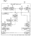
- Fig. 1 is a block diagram of an OFDM signal demodulator 12b in a first embodiment of the present invention. This OFDM signal demodulator 12b is included in the OFDM signal receiver 2 shown in Fig. 10.
- the quadrature demodulation circuit 21 frequency converts the iF band to the baseband by quadrature demodulation of the output from the tuner 11 in Fig. 10, converts real number signals to complex number signals of I components and Q components, and outputs the result to the Fourier transform circuit 22.
- the Fourier transform circuit 22 converts the output of the quadrature demodulation circuit 21 from the time domain to the frequency domain by Fourier transform, and outputs the result to the channel estimation circuit 23b and the first input of the divider 24.
- the channel estimation circuit 23b estimates the frequency response of the channel from the pilot signal contained in the output of the Fourier transform circuit 22, and the output of the estimation circuit 23b is then supplied to the second input of the divider 24.
- the divider 24 then compensates for amplitude and phase distortion introduced to the signal on the channel by dividing the output of the Fourier transform circuit 22 by the output of the channel estimation circuit 23b.
- the divider 24 outputs the result to the error correction circuit 25.
- the error correction circuit 25 applies error correction to the divider 24 output, and the output from the error correction circuit 25 is supplied as the output of the OFDM signal demodulator 12 to the source decoder 13 shown in Fig. 10.
- Error correction by this error correction circuit 25 could include de-mapping, deinterleaving, Viterbi decoding, energy dispersion, or Reed-Solomon decoding, for example.
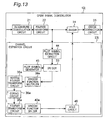
- the pilot signal extraction circuit 31 extracts the pilot signal contained in the output of the Fourier transform circuit 22, and outputs the result to the first input of a divider 33.
- the pilot signal generator 32 generates a pilot signal of known amplitude and phase synchronized to the pilot signal extraction circuit 31, and outputs the resulting pilot signal to the second input of the divider 33.
- the divider 33 then divides the output of the pilot signal extraction circuit 31 by the output of the pilot signal generator 32 to acquire the frequency response of the channel sampled at the pilot signal interval, and then outputs the result to the zero signal insertion circuit 34a.
- the zero signal insertion circuit 34a inserts a zero signal to the output of the divider 33, and outputs the result to a window function multiplier 39a.
- the window function multiplier 39a multiplies the output of the zero signal insertion circuit 34a by a window function, and outputs the result to the inverse Fourier transform circuit 35a.
- the inverse Fourier transform circuit 35a converts the frequency response output from the window function multiplier 39a to an impulse response by inverse Fourier transform, and outputs the result to the coring circuit 36a.
- the coring circuit 36a replaces data equal to or less than a specified threshold value in the output of the inverse Fourier transform circuit 35a with a zero signal, and outputs the result to the truncation circuit 37a.
- the truncation circuit 37a truncates the coring circuit output to a specified length and replaces other data with a zero signal to remove aliasing components (due to the frequency response, which is the input to the inverse Fourier transform circuit 35a, being sampled at the pilot signal period).
- the truncation circuit 37a outputs the result to the window function divider 40a.
- the window function divider 40a divides the output of the Fourier transform circuit 38a by the window function applied by the window function multiplier 39a.
- the output of the window function divider 40a is then supplied as the output of the channel estimation circuit 23b to the second input of the divider 24.
- the frequency response acquired by the Fourier transform circuit 38a applying Fourier transform to the output of the truncation circuit 37a is thus not only interpolated, but estimation error due to noise is reduced by the operation of the coring circuit 36a.
- window function multiplier 39a is located downstream of the zero signal insertion circuit 34a, but the window function multiplier 39a could be upstream of the zero signal insertion circuit 34a.
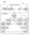
- Fig. 2 is a block diagram of an OFDM signal demodulator 12c in a second embodiment of the present invention. This OFDM signal demodulator 12c is included in the OFDM signal receiver 2 shown in Fig. 10. Like elements are identified by like reference numerals in Fig. 2 and Fig. 1, and further description thereof is omitted beiow.
- the output of the divider 33 is supplied to the zero signal insertion circuit 34a and time axis interpolation circuit 41.
- the time axis interpolation circuit 41 interpolates the frequency response (sampled at the pilot signal period) output from the divider 33 on the time axis, and outputs the result to the frequency axis interpolation circuit 42.
- the frequency axis interpolation circuit 42 interpolates the frequency response that was interpolated on the time axis by the time axis interpolation circuit 41 on the frequency axis, and outputs the result to the first input of selection circuit 43a.
- the window function divider 40a outputs to the second input of the selection circuit 43a.
- the selection circuit 43a selects the frequency response output from the window function divider 40a for carriers within a specific range of the signal band center, selects the frequency response output from the frequency axis interpolation circuit 42 for the remaining carriers near the signal band edges, and outputs the result to as the output of the channel estimation circuit 23c to the second input of the divider 24.
- Estimation error for the overall signal band can thus be reduced as a result of the selection circuit 43a selecting the frequency response in which estimation error caused by noise has been reduced by the operation from the zero signal insertion circuit 34a to the window function divider 40a for carriers near the signal band center, and selecting the frequency response interpolated by the time axis interpolation circuit 41 and frequency axis interpolation circuit 42 for carriers near the signal band edges where the frequency response is easily distorted.
- window function multiplier 39a is located downstream of the zero signal insertion circuit 34a, but the window function multiplier 39a could be upstream of the zero signal insertion circuit 34a.
- this embodiment of the invention can also be applied to implementations not having a window function multiplier 39a and window function divider 40a.
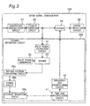
- Fig. 3 is a block diagram of an OFDM signal demodulator 12d in a third embodiment of the present invention. This OFDM signal demodulator 12d is included in the OFDM signal receiver 2 shown in Fig. 10. Like elements are identified by like reference numerals in Fig. 3 and Fig. 1, and further description thereof is omitted below.
- Fig. 3 the output of the divider 33 is supplied to the inverse Fourier transform circuit 35b.
- inverse Fourier transform circuit 35b converts the frequency response output from the divider 33 to an impulse response by an inverse Fourier transform, and outputs the result to coring circuit 36b.
- the coring circuit 36b applies a coring process to the output from the inverse Fourier transform circuit 35b, and outputs the result to Fourier transform circuit 38b.
- the Fourier transform circuit 38b converts the impulse response from the coring circuit 36b to a frequency response by Fourier transform, and outputs the result to the time axis interpolation circuit 41.
- the time axis interpolation circuit 41 interpolates the frequency response (sampled at the pilot signal period) output from the Fourier transform circuit 38b on the time axis, and outputs the result to the frequency axis interpolation circuit 42.
- the frequency axis interpolation circuit 42 interpolates the frequency response that was interpolated on the time axis by the time axis interpolation circuit 41 on the frequency axis, and outputs the result as the output of the channel estimation circuit 23d to the second input of the divider 24.
- This embodiment of the invention reduces the data processed by the inverse Fourier transform circuit 35b and Fourier transform circuit 38b as a result of not inserting zeroes before the inverse Fourier transform circuit 35b, and can therefore reduce the circuit scale needed for a hardware implementation and the number of operations performed in a software implementation.
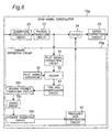
- time axis interpolation circuit 41 is located downstream of the Fourier transform circuit 38b in Fig. 3, but the time axis interpolation circuit 41 could be located before the inverse Fourier transform circuit 35c as shown in Fig. 6.
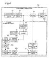
- Fig. 4 is a block diagram of an OFDM signal demodulator 12e in a fourth embodiment of the present invention.
- This OFDM signal demodulator 12e is included in the OFDM signal receiver 2 shown in Fig. 10.
- Like elements are identified by like reference numerals in Fig. 4 and Fig. 3, and further description thereof is omitted below.
- Fig. 4 the output of the divider 33 is supplied to the window function multiplier 39b.
- the window function multiplier 39b multiplies the output of the divider 33 with a window function, and outputs the result to inverse Fourier transform circuit 35b.
- the output of the Fourier transform circuit 38b is supplied to the window function divider 40b.
- the window function divider 40b divides the output of the Fourier transform circuit 38b by the window function applied by the window function multiplier 39b, and outputs the result to the time axis interpolation circuit 41.
- This embodiment of the invention reduces the data processed by the inverse Fourier transform circuit 35b and Fourier transform circuit 38b as a result of not inserting zeroes before the inverse Fourier transform circuit 35b, and can therefore reduce the circuit scale needed for a hardware implementation and the number of operations performed in a software implementation.
- the number of signal components replaced by zero signals in the coring circuit 36b is reduced because the side lobe components of the impulse response output from the inverse Fourier transform circuit 35b are suppressed as a result of the window function multiplier 39b applying a window function. Distortion of the frequency response acquired as the output of the Fourier transform circuit 38b can thus be reduced.
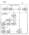
- time axis interpolation circuit 41 is disposed downstream of the window function divider 40b in Fig. 4, but the time axis interpolation circuit 41 could be located before the window function multiplier 39c as shown in Fig. 7.
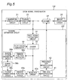
- Fig. 5 is a block diagram of an OFDM signal demodulator 12f in a fifth embodiment of the present invention. This OFDM signal demodulator 12f is included in the OFDM signal receiver 2 shown in Fig. 10. Like elements are identified by like reference numerals in Fig. 5 and Fig. 4, and further description thereof is omitted below.
- Fig. 5 the output of the divider 33 is supplied to the window function multiplier 39b and the first input of the selection circuit 43b.
- the output of the window function divider 40b is supplied to the second input of the selection circuit 43b.
- the selection circuit 43b selects the frequency response output from the window function divider 40b for carriers within a specific range of the signal band center, selects the frequency response output from the divider 33 for the remaining carriers near the signal band edges, and outputs the result to the time axis interpolation circuit 41.
- This embodiment of the invention reduces the data processed by the inverse Fourier transform circuit 35b and Fourier transform circuit 38b as a result of not inserting zeroes before the inverse Fourier transform circuit 35b, and can therefore reduce the circuit scale needed for a hardware implementation and the number of operations performed in a software implementation.
- estimation error for the overall signal band can be reduced as a result of the selection circuit 43b selecting the frequency response in which estimation error caused by noise has been reduced by the operation from the window function multiplier 39b to the window function divider 40b for carriers near the signal band center, and selecting the frequency response acquired by the divider 33 for carriers near the signal band edges where the frequency response is easily distorted.
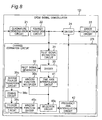
- time axis interpolation circuit 41 is located after the selection circuit 43b in Fig. 5, but the time axis interpolation circuit 41 could be located upstream of the window function multiplier 39c and selection circuit 43c as shown in Fig. 8.
- Fig. 13 is a block diagram of an OFDM signal demodulator 12j in a sixth embodiment of the present invention. This OFDM signal demodulator 12j is included in the OFDM signal receiver 2 shown in Fig. 10.
- This embodiment of the invention applies to wireless LAN (local area network) systems that transmit finite length frames and send a pilot symbol containing the known amplitude and phase of all carriers in the preamble such as defined in IEEE (Institute of Electrical and Electronics Engineering) 802.11 a, and to systems such as the European terrestrial digital audio broadcasting (DAB) system that transmit continuous frames and insert a pilot symbol of known amplitude and phase for all carriers every frame period.
- wireless LAN local area network
- DAB European terrestrial digital audio broadcasting
- the quadrature demodulation circuit 21 frequency converts the IF band to the baseband by quadrature demodulation of the output from the tuner 11 in Fig. 10, converts real number signals to complex number signals of I components and Q components, and outputs the result to the Fourier transform circuit 22.
- the Fourier transform circuit 22 converts the output of the quadrature demodulation circuit 21 from the time domain to the frequency domain by Fourier transform, and outputs the result to the channel estimation circuit 23j and the first input of the divider 24.
- the channel estimation circuit 23j estimates the frequency response of the channel from the pilot symbol contained in the output of the Fourier transform circuit 22, and the output of the estimation circuit 23j is then supplied to the second input of the divider 24.
- the divider 24 then compensates for amplitude and phase distortion introduced to the signal on the channel by dividing the output of the Fourier transform circuit 22 by the output of the channel estimation circuit 23j.
- the divider 24 outputs the result to the error correction circuit 25.
- the error correction circuit 25 applies error correction to the divider 24 output, and the output from the error correction circuit 25 is supplied as the output of the OFDM signal demodulator 12j to the source decoder 13 shown in Fig. 10.
- Error correction by this error correction circuit 25 could include de-mapping, deinterleaving, Viterbi decoding, energy dispersion, or Reed-Solomon decoding, for example.
- the pilot symbol extraction circuit 44 extracts the pilot symbol contained in the output of the Fourier transform circuit 22, and outputs the result to the first input of a divider 33.
- the pilot symbol generator 45 generates a pilot symbol of known amplitude and phase for all carriers synchronized to the pilot symbol extraction circuit 44, and outputs the result to the second input of the divider 33.
- the divider 33 then divides the output of the pilot symbol extraction circuit 44 by the output of the pilot symbol generator 45 to acquire the frequency response of the channel, and then outputs the result to the window function multiplier 39a.
- the window function multiplier 39a multiplies the output of the divider 33 by a window function, and outputs the result to inverse Fourier transform circuit 35a.
- the inverse Fourier transform circuit 35a converts the frequency response output from the window function multiplier 39a to an impulse response by inverse Fourier transform, and outputs the result to the coring circuit 36a.
- the coring circuit 36a replaces data equal to or less than a specified threshold value in the output of the inverse Fourier transform circuit 35a with a zero signal, and outputs the result to the Fourier transform circuit 38a.
- the Fourier transform circuit 38a converts the impulse response output from the coring circuit 36a to a frequency response by Fourier transform, and outputs the result to the window function divider 40a.
- the window function divider 40a divides the output of the Fourier transform circuit 38a by the window function applied by the window function multiplier 39a, and outputs the result to hold circuit 46.
- This hold circuit 46 holds the output of the window function divider 40a until the end of the frame in a system such as IEEE 802.11a using finite length frames and transmitting the pilot symbol in the preamble, or for the frame period in a system such as DAB using continuous frames with the pilot symbol transmitted each frame period.
- the output of the hold circuit 46 is then supplied as the output of the channel estimation circuit 23j to the second input of the divider 24.
- the operation of the coring circuit 36a in this embodiment of the invention thus reduces estimation error due to noise in the frequency response acquired by the Fourier transform applied by the Fourier transform circuit 38a to the output of the coring circuit 36a.
- the hold circuit 46 could compensate for variation in amplitude and phase using the pilot signal.
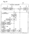
- Fig. 14 is a block diagram of an OFDM signal demodulator 1 2k in a seventh embodiment of the present invention. This OFDM signal demodulator 12k is included in the OFDM signal receiver 2 shown in Fig. 10. Like elements are identified by like reference numerals in Fig. 14 and Fig. 13, and further description thereof is omitted below.
- Fig. 14 the output of the divider 33 is supplied to the window function multiplier 39a and the first input of the selection circuit 43a.
- the output of the window function divider 40a is supplied to the second input to the selection circuit 43a.
- the selection circuit 43a selects the frequency response output from the window function divider 40a for carriers within a specific range of the signal band center, selects the frequency response output from the divider 33 for the remaining carriers near the signal band edges, and outputs the result to the hold circuit 46.
- Estimation error for the overall signal band can thus be reduced as a result of the selection circuit 43a selecting the frequency response in which estimation error caused by noise has been reduced by the operation from the window function multiplier 39a to the window function divider 40a for carriers near the signal band center, and selecting the frequency response calculated by the divider 33 for carriers near the signal band edges where the frequency response is easily distorted.
- the threshold values used in the coring circuits 36a, 36b, 36c in the foregoing embodiments can be a fixed value or can be appropriately controlled. Methods of appropriately controlling this threshold value include controlling the threshold value according to the impulse response, or according to the noise level.
- the window function applied by the window function multipliers 39a, 39b, 39c and the window function dividers 40a, 40b, 40c in the foregoing embodiments is preferably a function, such as a Hamming window, Hanning window, or Blackman window, that can suppress side lobe components.
- transmission systems such as DVB-T or ISDB-T that include a pilot signal dispersed in the signal band, a transmission system such as IEEE 802.11 a using finite length frames and transmit the pilot symbol in the preamble, or a transmission system such as DAB using continuous frames with the pilot symbol transmitted each frame period, but other transmission methods that send a pilot signal of known amplitude and phase could be used.
- the position of the AD (analog to digital) converter used for digital signal processing in the OFDM signal demodulator is not specifically related to the operating principle of the present invention, and the same principle can be applied regardless of where the AD converter is inserted.
- An OFDM signal receiving apparatus improves reception performance by reducing frequency response estimation error, and reduces the circuit scale needed for a hardware implementation and the number of operations performed in a software implementation.
- the OFDM signal receiving apparatus of this invention can therefore be beneficially used as a digital broadcast receiver, wireless LAN modem, cell phone, or other wireless communication terminal.
- the invention can also be used in wired communication modems connected to a telephone line, power line, coaxial cable, or optical fiber, for example.
Landscapes
- Engineering & Computer Science (AREA)
- Computer Networks & Wireless Communication (AREA)
- Signal Processing (AREA)
- Physics & Mathematics (AREA)
- Nonlinear Science (AREA)
- Power Engineering (AREA)
- Cable Transmission Systems, Equalization Of Radio And Reduction Of Echo (AREA)
- Noise Elimination (AREA)
- Radio Relay Systems (AREA)
Applications Claiming Priority (2)
| Application Number | Priority Date | Filing Date | Title |
|---|---|---|---|
| JP2003342990 | 2003-10-01 | ||
| JP2003342990 | 2003-10-01 |
Publications (2)
| Publication Number | Publication Date |
|---|---|
| EP1521413A2 true EP1521413A2 (fr) | 2005-04-06 |
| EP1521413A3 EP1521413A3 (fr) | 2009-09-30 |
Family
ID=34309104
Family Applications (1)
| Application Number | Title | Priority Date | Filing Date |
|---|---|---|---|
| EP04023312A Withdrawn EP1521413A3 (fr) | 2003-10-01 | 2004-09-30 | Réception multiporteuse à estimation de canal et égalisation |
Country Status (3)
| Country | Link |
|---|---|
| US (1) | US7535820B2 (fr) |
| EP (1) | EP1521413A3 (fr) |
| CN (1) | CN1604579B (fr) |
Cited By (5)
| Publication number | Priority date | Publication date | Assignee | Title |
|---|---|---|---|---|
| WO2005081486A1 (fr) * | 2004-02-19 | 2005-09-01 | Nokia Corporation | Procede et appareil fournissant une estimation de canal interpole dans le domaine temporel avec une suppression de bruit avancee pour transmissions multiporteuses |
| WO2006019709A1 (fr) * | 2004-07-20 | 2006-02-23 | Qualcomm Incorporated | Filtrage de domaine de frequence destine a ameliorer l'estimation de canal dans des systemes a porteuses multiples |
| CN102308541A (zh) * | 2009-02-04 | 2012-01-04 | 阿科恩科技公司 | 用于ofdm系统的两步式最小二乘时域信道估计 |
| EP2022204A4 (fr) * | 2006-06-01 | 2014-03-05 | Qualcomm Inc | Estimation de canal améliorée pour récepteur de système de communication |
| EP1924040A3 (fr) * | 2006-11-15 | 2014-04-02 | Fujitsu Ltd. | Dispositif d'estimation de canal |
Families Citing this family (29)
| Publication number | Priority date | Publication date | Assignee | Title |
|---|---|---|---|---|
| CN100566317C (zh) * | 2004-10-22 | 2009-12-02 | 财团法人工业技术研究院 | 基于频率相关性的相干正交频分复用接收器同步方法与装置 |
| US20060088133A1 (en) * | 2004-10-22 | 2006-04-27 | Industrial Technology Research Institute | Time-frequency correlation-based synchronization for coherent OFDM receiver |
| US7848463B2 (en) * | 2005-04-07 | 2010-12-07 | Qualcomm Incorporated | Adaptive time-filtering for channel estimation in OFDM system |
| KR100724949B1 (ko) * | 2005-05-03 | 2007-06-04 | 삼성전자주식회사 | 주파수 분할 다중접속 기반 무선통신 시스템에서 데이터와제어 정보의 다중화 방법 및 장치 |
| LV13342B (en) * | 2005-05-18 | 2005-10-20 | Real Sound Lab Sia | Method and device for correction of acoustic parameters of electro-acoustic transducers |
| CN100481826C (zh) * | 2005-10-20 | 2009-04-22 | 清华大学 | 一种正交频分复用系统信号发送及接收方法 |
| CN101331728B (zh) * | 2005-12-13 | 2011-08-03 | 松下电器产业株式会社 | 发送电路和采用该发送电路的通信装置 |
| JP4958565B2 (ja) * | 2006-01-06 | 2012-06-20 | パナソニック株式会社 | 無線通信装置 |
| JP4944106B2 (ja) * | 2006-05-25 | 2012-05-30 | シャープ株式会社 | 受信機および伝搬路推定方法 |
| US8000224B2 (en) | 2006-06-07 | 2011-08-16 | Sharp Kabushiki Kaisha | Receiver and frequency information estimating method |
| JP4215084B2 (ja) * | 2006-09-13 | 2009-01-28 | 沖電気工業株式会社 | 等化器及び等化方法 |
| US8787499B2 (en) * | 2007-03-27 | 2014-07-22 | Qualcomm Incorporated | Channel estimation with effective co-channel interference suppression |
| EP2164198B1 (fr) * | 2007-06-22 | 2017-08-09 | Panasonic Intellectual Property Management Co., Ltd. | Dispositif de transmission, dispositif de réception et procédé de transmission ofdm |
| US20090059782A1 (en) * | 2007-08-29 | 2009-03-05 | Rgb Systems, Inc. | Method and apparatus for extending the transmission capability of twisted pair communication systems |
| US7746761B2 (en) * | 2007-10-25 | 2010-06-29 | Nokia Siemens Networks Oy | Techniques to generate constant envelope multicarrier transmission for wireless networks |
| US20090147669A1 (en) * | 2007-12-10 | 2009-06-11 | Nokia Siemens Networks Oy | Continuous phase modulation encoder for wireless networks |
| US7804376B2 (en) * | 2007-12-13 | 2010-09-28 | Nokia Siemens Networks Oy | Continuous phase modulation processing for wireless networks |
| US7698098B2 (en) * | 2008-02-18 | 2010-04-13 | Thermo Electron Scientific Instruments Llc | Efficient spectral matching, particularly for multicomponent spectra |
| US8699529B2 (en) * | 2008-03-28 | 2014-04-15 | Qualcomm Incorporated | Broadband pilot channel estimation using a reduced order FFT and a hardware interpolator |
| US8630364B2 (en) * | 2008-07-25 | 2014-01-14 | Nokia Siemens Networks Oy | Termination techniques for multi-index continuous phase encoders for wireless networks |
| US8089858B2 (en) * | 2008-08-14 | 2012-01-03 | Sony Corporation | Frame and signalling pattern structure for multi-carrier systems |
| US20100124292A1 (en) * | 2008-11-20 | 2010-05-20 | Advanced Micro Devices, Inc. | Method and System for Receiver Synchronization |
| JPWO2011108429A1 (ja) * | 2010-03-05 | 2013-06-27 | 日本電気株式会社 | チャネル推定回路、チャネル推定方法および受信機 |
| US8406343B2 (en) * | 2010-08-25 | 2013-03-26 | Intel Corporation | Methods and systems to resolve cyclic ambiguity of a channel impulse response |
| CA2803906C (fr) | 2010-12-10 | 2018-10-30 | Panasonic Corporation | Procede de generation de signaux et dispositif de generation de signaux |
| US9203656B2 (en) * | 2012-08-08 | 2015-12-01 | Mitsubishi Electric Corporation | Receiver and method of estimating frequency response of transmission path by receiver |
| US9112567B2 (en) * | 2013-11-19 | 2015-08-18 | Symbol Technologies, Llc | Apparatus and method for compensation of AM noise in RFID devices through modulation of a received signal |
| KR101911275B1 (ko) | 2014-12-31 | 2018-10-24 | 엘지전자 주식회사 | 방송 신호 송신 장치, 방송 신호 수신 장치, 방송 신호 송신 방법, 및 방송 신호 수신 방법 |
| JP7361549B2 (ja) * | 2019-09-18 | 2023-10-16 | Kddi株式会社 | 受信装置及びプログラム |
Family Cites Families (15)
| Publication number | Priority date | Publication date | Assignee | Title |
|---|---|---|---|---|
| FR2671923B1 (fr) * | 1991-01-17 | 1993-04-16 | France Etat | Dispositif de demodulation coherente de donnees numeriques entrelacees en temps et en frequence, a estimation de la reponse frequentielle du canal de transmission et seuillage, et emetteur correspondant. |
| JP2772286B2 (ja) | 1996-08-30 | 1998-07-02 | 株式会社次世代デジタルテレビジョン放送システム研究所 | 直交周波数分割多重信号復調装置 |
| US6643275B1 (en) * | 1998-05-15 | 2003-11-04 | Telefonaktiebolaget Lm Ericsson (Publ) | Random access in a mobile telecommunications system |
| US6654429B1 (en) * | 1998-12-31 | 2003-11-25 | At&T Corp. | Pilot-aided channel estimation for OFDM in wireless systems |
| JP3787041B2 (ja) | 1999-06-01 | 2006-06-21 | 日本放送協会 | 回り込みキャンセラ |
| JP4460738B2 (ja) | 2000-08-21 | 2010-05-12 | 株式会社ケンウッド | 直交周波数分割多重信号受信装置及び直交周波数分割多重信号受信方法 |
| KR100510434B1 (ko) * | 2001-04-09 | 2005-08-26 | 니폰덴신뎅와 가부시키가이샤 | Ofdm신호전달 시스템, ofdm신호 송신장치 및ofdm신호 수신장치 |
| EP1263179B1 (fr) * | 2001-05-29 | 2007-06-27 | Lucent Technologies Inc. | Estimation de canal dans un système CDMA utilisant des symboles de service codés comme symboles pilotes supplémentaires |
| EP1276288B1 (fr) * | 2001-07-10 | 2007-01-10 | Sony Deutschland GmbH | Symboles de référence pour l'estimation de canal pour la transmission multiporteuse |
| KR100833223B1 (ko) * | 2001-07-11 | 2008-05-28 | 삼성전자주식회사 | 보호 구간을 이용해 심볼 타이밍 동기를 수행하는ofdm 수신 시스템 및 그 방법 |
| JP2003101503A (ja) | 2001-09-21 | 2003-04-04 | Mega Chips Corp | Ofdm用等化装置およびofdm用等化方法 |
| JP3910453B2 (ja) | 2002-01-23 | 2007-04-25 | 三菱電機株式会社 | 受信装置および伝送路推定方法 |
| US7099270B2 (en) * | 2002-06-06 | 2006-08-29 | Texas Instruments Incorporated | Multi-path equalization for orthogonal frequency division multiplexing communication system |
| CN1207908C (zh) * | 2002-08-16 | 2005-06-22 | 清华大学 | 基于滑动窗口的对含导频的块信号的信道估计和均衡方法 |
| JP4109530B2 (ja) | 2002-10-24 | 2008-07-02 | 松下電器産業株式会社 | 回り込みキャンセラ |
-
2004
- 2004-09-30 EP EP04023312A patent/EP1521413A3/fr not_active Withdrawn
- 2004-10-01 US US10/954,614 patent/US7535820B2/en active Active
- 2004-10-08 CN CN200410084973.4A patent/CN1604579B/zh not_active Expired - Lifetime
Cited By (9)
| Publication number | Priority date | Publication date | Assignee | Title |
|---|---|---|---|---|
| WO2005081486A1 (fr) * | 2004-02-19 | 2005-09-01 | Nokia Corporation | Procede et appareil fournissant une estimation de canal interpole dans le domaine temporel avec une suppression de bruit avancee pour transmissions multiporteuses |
| US7412005B2 (en) | 2004-02-19 | 2008-08-12 | Nokia Corporation | Method and apparatus providing time domain interpolated channel estimation with advanced noise suppression for multicarrier transmissions |
| WO2006019709A1 (fr) * | 2004-07-20 | 2006-02-23 | Qualcomm Incorporated | Filtrage de domaine de frequence destine a ameliorer l'estimation de canal dans des systemes a porteuses multiples |
| JP2008507902A (ja) * | 2004-07-20 | 2008-03-13 | クゥアルコム・インコーポレイテッド | マルチキャリアシステム内のチャネル推定を改善するための周波数領域フィルタリング |
| US7616711B2 (en) | 2004-07-20 | 2009-11-10 | Qualcomm Incorporated | Frequency domain filtering to improve channel estimation in multicarrier systems |
| EP2022204A4 (fr) * | 2006-06-01 | 2014-03-05 | Qualcomm Inc | Estimation de canal améliorée pour récepteur de système de communication |
| EP1924040A3 (fr) * | 2006-11-15 | 2014-04-02 | Fujitsu Ltd. | Dispositif d'estimation de canal |
| CN102308541A (zh) * | 2009-02-04 | 2012-01-04 | 阿科恩科技公司 | 用于ofdm系统的两步式最小二乘时域信道估计 |
| CN102308541B (zh) * | 2009-02-04 | 2016-05-25 | 阿科恩科技公司 | 用于ofdm系统的两步式最小二乘时域信道估计 |
Also Published As
| Publication number | Publication date |
|---|---|
| US20050073949A1 (en) | 2005-04-07 |
| US7535820B2 (en) | 2009-05-19 |
| CN1604579A (zh) | 2005-04-06 |
| EP1521413A3 (fr) | 2009-09-30 |
| CN1604579B (zh) | 2010-04-28 |
Similar Documents
| Publication | Publication Date | Title |
|---|---|---|
| US7535820B2 (en) | OFDM signal receiving apparatus and OFDM signal receiving method | |
| JP4555652B2 (ja) | Ofdm信号受信装置及びofdm信号受信方法 | |
| US6449245B1 (en) | Signal receiving apparatus and method and providing medium | |
| EP1791314B1 (fr) | Procédé et appareil de synchronisation de la fréquence porteuse dans un système à porteuses multiples | |
| US9742611B2 (en) | Synchronizing orthogonal frequency division multiplexed (OFDM) symbols in a receiver | |
| US7920462B2 (en) | Amplitude attenuation estimation and recovery systems for OFDM signal used in communication systems | |
| EP2018725A2 (fr) | Système et procédé de calcul de variance du bruit | |
| US9942076B2 (en) | Device and method for detecting and recovering payload data from a signal | |
| EP2346222A2 (fr) | Appareil et procédé de réception, programme et système de réception | |
| WO2007131056A2 (fr) | Correction de phase dans un récepteur d'essai | |
| EP2157753B1 (fr) | Réglage d'interpolation pour l'estimation de canal | |
| US20240333564A1 (en) | Radio receiver with offset compensation loops and related methods | |
| JP4373757B2 (ja) | 受信装置、受信方法、集積回路、及びプログラム | |
| JP2008502282A (ja) | 直交周波数分割多重受信器 | |
| EP2720426B1 (fr) | Procédé et dispositif pour correction de décalage de fréquence sur symboles reçus | |
| EP1330087A2 (fr) | Récupération de l'horloge de symboles pour récepteurs multiporteuses | |
| US20090097596A1 (en) | Methods and Systems for Impulse Noise Compensation for OFDM Systems | |
| JP2003229831A (ja) | Ofdm信号受信装置 | |
| US20110268172A1 (en) | Receiver apparatus and receiving method | |
| JP3756121B2 (ja) | Ofdm復調装置及び電力重み付け方法 | |
| EP1528741A1 (fr) | Procédé et dispositif pour réception diversité dans un système OFDM | |
| CN101567868A (zh) | 一种cmmb制式手机电视小数频偏估计方法 | |
| US7710858B1 (en) | Apparatus, system, and method for sample timing synchronization in a receiver | |
| US20150092891A1 (en) | Methods and Systems for Fine Timing Synchronization | |
| US8699632B2 (en) | OFDM reception device, OFDM reception circuit, OFDM reception method, and OFDM reception program |
Legal Events
| Date | Code | Title | Description |
|---|---|---|---|
| PUAI | Public reference made under article 153(3) epc to a published international application that has entered the european phase |
Free format text: ORIGINAL CODE: 0009012 |
|
| AK | Designated contracting states |
Kind code of ref document: A2 Designated state(s): AT BE BG CH CY CZ DE DK EE ES FI FR GB GR HU IE IT LI LU MC NL PL PT RO SE SI SK TR |
|
| AX | Request for extension of the european patent |
Extension state: AL HR LT LV MK |
|
| RAP1 | Party data changed (applicant data changed or rights of an application transferred) |
Owner name: PANASONIC CORPORATION |
|
| PUAL | Search report despatched |
Free format text: ORIGINAL CODE: 0009013 |
|
| AK | Designated contracting states |
Kind code of ref document: A3 Designated state(s): AT BE BG CH CY CZ DE DK EE ES FI FR GB GR HU IE IT LI LU MC NL PL PT RO SE SI SK TR |
|
| AX | Request for extension of the european patent |
Extension state: AL HR LT LV MK |
|
| 17P | Request for examination filed |
Effective date: 20100222 |
|
| 17Q | First examination report despatched |
Effective date: 20100423 |
|
| AKX | Designation fees paid |
Designated state(s): DE FR GB |
|
| RAP1 | Party data changed (applicant data changed or rights of an application transferred) |
Owner name: PANASONIC INTELLECTUAL PROPERTY CORPORATION OF AME |
|
| STAA | Information on the status of an ep patent application or granted ep patent |
Free format text: STATUS: THE APPLICATION HAS BEEN WITHDRAWN |
|
| 18W | Application withdrawn |
Effective date: 20141027 |