EP1523032B1 - Procédé de fabrication d'une structure à couche en oxide de carbure de silicium - Google Patents
Procédé de fabrication d'une structure à couche en oxide de carbure de silicium Download PDFInfo
- Publication number
- EP1523032B1 EP1523032B1 EP04023713A EP04023713A EP1523032B1 EP 1523032 B1 EP1523032 B1 EP 1523032B1 EP 04023713 A EP04023713 A EP 04023713A EP 04023713 A EP04023713 A EP 04023713A EP 1523032 B1 EP1523032 B1 EP 1523032B1
- Authority
- EP
- European Patent Office
- Prior art keywords
- group element
- oxide layer
- gas
- layer
- sic
- Prior art date
- Legal status (The legal status is an assumption and is not a legal conclusion. Google has not performed a legal analysis and makes no representation as to the accuracy of the status listed.)
- Expired - Lifetime
Links
Images






Classifications
-
- H—ELECTRICITY
- H10—SEMICONDUCTOR DEVICES; ELECTRIC SOLID-STATE DEVICES NOT OTHERWISE PROVIDED FOR
- H10D—INORGANIC ELECTRIC SEMICONDUCTOR DEVICES
- H10D64/00—Electrodes of devices having potential barriers
- H10D64/60—Electrodes characterised by their materials
- H10D64/66—Electrodes having a conductor capacitively coupled to a semiconductor by an insulator, e.g. MIS electrodes
- H10D64/68—Electrodes having a conductor capacitively coupled to a semiconductor by an insulator, e.g. MIS electrodes characterised by the insulator, e.g. by the gate insulator
- H10D64/693—Electrodes having a conductor capacitively coupled to a semiconductor by an insulator, e.g. MIS electrodes characterised by the insulator, e.g. by the gate insulator the insulator comprising nitrogen, e.g. nitrides, oxynitrides or nitrogen-doped materials
-
- H—ELECTRICITY
- H10—SEMICONDUCTOR DEVICES; ELECTRIC SOLID-STATE DEVICES NOT OTHERWISE PROVIDED FOR
- H10D—INORGANIC ELECTRIC SEMICONDUCTOR DEVICES
- H10D12/00—Bipolar devices controlled by the field effect, e.g. insulated-gate bipolar transistors [IGBT]
- H10D12/01—Manufacture or treatment
- H10D12/031—Manufacture or treatment of IGBTs
-
- H—ELECTRICITY
- H10—SEMICONDUCTOR DEVICES; ELECTRIC SOLID-STATE DEVICES NOT OTHERWISE PROVIDED FOR
- H10D—INORGANIC ELECTRIC SEMICONDUCTOR DEVICES
- H10D30/00—Field-effect transistors [FET]
- H10D30/01—Manufacture or treatment
- H10D30/021—Manufacture or treatment of FETs having insulated gates [IGFET]
- H10D30/028—Manufacture or treatment of FETs having insulated gates [IGFET] of double-diffused metal oxide semiconductor [DMOS] FETs
- H10D30/0291—Manufacture or treatment of FETs having insulated gates [IGFET] of double-diffused metal oxide semiconductor [DMOS] FETs of vertical DMOS [VDMOS] FETs
- H10D30/0295—Manufacture or treatment of FETs having insulated gates [IGFET] of double-diffused metal oxide semiconductor [DMOS] FETs of vertical DMOS [VDMOS] FETs using recessing of the source electrodes
-
- H—ELECTRICITY
- H10—SEMICONDUCTOR DEVICES; ELECTRIC SOLID-STATE DEVICES NOT OTHERWISE PROVIDED FOR
- H10D—INORGANIC ELECTRIC SEMICONDUCTOR DEVICES
- H10D30/00—Field-effect transistors [FET]
- H10D30/60—Insulated-gate field-effect transistors [IGFET]
- H10D30/63—Vertical IGFETs
-
- H—ELECTRICITY
- H10—SEMICONDUCTOR DEVICES; ELECTRIC SOLID-STATE DEVICES NOT OTHERWISE PROVIDED FOR
- H10D—INORGANIC ELECTRIC SEMICONDUCTOR DEVICES
- H10D30/00—Field-effect transistors [FET]
- H10D30/60—Insulated-gate field-effect transistors [IGFET]
- H10D30/63—Vertical IGFETs
- H10D30/635—Vertical IGFETs having no inversion channels, e.g. vertical accumulation channel FETs [ACCUFET] or normally-on vertical IGFETs
-
- H—ELECTRICITY
- H10—SEMICONDUCTOR DEVICES; ELECTRIC SOLID-STATE DEVICES NOT OTHERWISE PROVIDED FOR
- H10D—INORGANIC ELECTRIC SEMICONDUCTOR DEVICES
- H10D62/00—Semiconductor bodies, or regions thereof, of devices having potential barriers
- H10D62/80—Semiconductor bodies, or regions thereof, of devices having potential barriers characterised by the materials
- H10D62/83—Semiconductor bodies, or regions thereof, of devices having potential barriers characterised by the materials being Group IV materials, e.g. B-doped Si or undoped Ge
- H10D62/832—Semiconductor bodies, or regions thereof, of devices having potential barriers characterised by the materials being Group IV materials, e.g. B-doped Si or undoped Ge being Group IV materials comprising two or more elements, e.g. SiGe
- H10D62/8325—Silicon carbide
-
- H—ELECTRICITY
- H10—SEMICONDUCTOR DEVICES; ELECTRIC SOLID-STATE DEVICES NOT OTHERWISE PROVIDED FOR
- H10D—INORGANIC ELECTRIC SEMICONDUCTOR DEVICES
- H10D64/00—Electrodes of devices having potential barriers
- H10D64/01—Manufacture or treatment
- H10D64/013—Manufacture or treatment of electrodes having a conductor capacitively coupled to a semiconductor by an insulator
- H10D64/01366—Manufacture or treatment of electrodes having a conductor capacitively coupled to a semiconductor by an insulator the semiconductor being silicon carbide
-
- H—ELECTRICITY
- H10—SEMICONDUCTOR DEVICES; ELECTRIC SOLID-STATE DEVICES NOT OTHERWISE PROVIDED FOR
- H10D—INORGANIC ELECTRIC SEMICONDUCTOR DEVICES
- H10D64/00—Electrodes of devices having potential barriers
- H10D64/60—Electrodes characterised by their materials
- H10D64/66—Electrodes having a conductor capacitively coupled to a semiconductor by an insulator, e.g. MIS electrodes
- H10D64/68—Electrodes having a conductor capacitively coupled to a semiconductor by an insulator, e.g. MIS electrodes characterised by the insulator, e.g. by the gate insulator
- H10D64/681—Electrodes having a conductor capacitively coupled to a semiconductor by an insulator, e.g. MIS electrodes characterised by the insulator, e.g. by the gate insulator having a compositional variation, e.g. multilayered
- H10D64/685—Electrodes having a conductor capacitively coupled to a semiconductor by an insulator, e.g. MIS electrodes characterised by the insulator, e.g. by the gate insulator having a compositional variation, e.g. multilayered being perpendicular to the channel plane
-
- H—ELECTRICITY
- H10—SEMICONDUCTOR DEVICES; ELECTRIC SOLID-STATE DEVICES NOT OTHERWISE PROVIDED FOR
- H10D—INORGANIC ELECTRIC SEMICONDUCTOR DEVICES
- H10D64/00—Electrodes of devices having potential barriers
- H10D64/20—Electrodes characterised by their shapes, relative sizes or dispositions
- H10D64/23—Electrodes carrying the current to be rectified, amplified, oscillated or switched, e.g. sources, drains, anodes or cathodes
- H10D64/251—Source or drain electrodes for field-effect devices
- H10D64/252—Source or drain electrodes for field-effect devices for vertical or pseudo-vertical devices
- H10D64/2527—Source or drain electrodes for field-effect devices for vertical or pseudo-vertical devices for vertical devices wherein the source or drain electrodes are recessed in semiconductor bodies
-
- H—ELECTRICITY
- H10—SEMICONDUCTOR DEVICES; ELECTRIC SOLID-STATE DEVICES NOT OTHERWISE PROVIDED FOR
- H10D—INORGANIC ELECTRIC SEMICONDUCTOR DEVICES
- H10D64/00—Electrodes of devices having potential barriers
- H10D64/20—Electrodes characterised by their shapes, relative sizes or dispositions
- H10D64/23—Electrodes carrying the current to be rectified, amplified, oscillated or switched, e.g. sources, drains, anodes or cathodes
- H10D64/251—Source or drain electrodes for field-effect devices
- H10D64/256—Source or drain electrodes for field-effect devices for lateral devices wherein the source or drain electrodes are recessed in semiconductor bodies
Definitions
- a thermal treatment at 950°C or higher in the gate electrode formation process deteriorates the actual channel mobility to 20 cm 2 /Vs or lower.
- a MISFET formed on a 4H-SiC (0 0 0 1) substrate having poor flatness, i.e., having steps over the surface, according to the above-described standard process has the channel mobility of 10 cm 2 /Vs or lower.
- the channel mobility over the surface of the SiC substrate has a large anisotropy.
- a large electric current flows along the steps whereas an electric current which traverses the steps is smaller by an order of magnitude than the large electric current flowing along the steps.
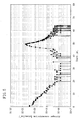
- E-Ev 0.3 eV to 0.4 eV.
- the interface state density of 1 ⁇ 10 12 cm -2 ⁇ eV -1 or lower was obtained in the potential range near each band edge.
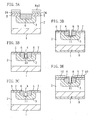
- the average nitrogen concentration in the entire gate insulating film (V-group element containing oxide layer) 7 was 8.3 ⁇ 10 19 cm -3 .
Landscapes
- Formation Of Insulating Films (AREA)
- Insulated Gate Type Field-Effect Transistor (AREA)
Claims (5)
- Procédé permettant de former une structure en couches d'oxyde de carbure de silicium, comprenant :l'étape (a) consistant à former une couche d'oxyde sur la surface d'une couche de carbure de silicium, etaprès l'étape (a), l'étape (b) consistant à placer la structure formée à l'étape (a) dans une chambre et à exposer la couche d'oxyde à une atmosphère incluant du NO ou un gaz contenant un élément du groupe V différent de l'azote à une température supérieure à 1100 °C et inférieure à 1250 °C de telle sorte que la couche d'oxyde se change en un élément du groupe V contenant une couche d'oxyde qui présente une constante diélectrique relative de 3,0 ou plus,dans lequel l'étape (b) est effectuée sous une atmosphère à pression réduite supérieure ou égale à 6,67 × 10⁴ Pa ou inférieure à 5,33 × 10⁴ Pa,caractérisé en ce quel'étape (b) est effectuée tout en faisant s'écouler le gaz de NO ou le gaz contenant un élément du groupe V différent de l'azote dans la chambre.
- Procédé selon la revendication 1, dans lequel l'étape (a) inclut l'étape consistant à former une couche d'oxyde par oxydation thermique et à effectuer un recuit de la couche d'oxyde dans une atmosphère de gaz inerte.
- Procédé selon la revendication 2, dans lequel l'étape (a) inclut l'oxydation dans une atmosphère de gaz oxydant à une température supérieure ou égale à 850 °C et inférieure ou égale à 950 °C après le recuit dans l'atmosphère de gaz inerte.
- Procédé selon la revendication 1, dans lequel le gaz contenant l'élément du groupe V contient de l'azote ou du phosphore.
- Procédé selon la revendication 4, dans lequel au moins l'un sélectionné à partir du gaz NO et du gaz PH3 est utilisé comme gaz contenant l'élément du groupe V.
Applications Claiming Priority (2)
| Application Number | Priority Date | Filing Date | Title |
|---|---|---|---|
| JP2003350244 | 2003-10-09 | ||
| JP2003350244 | 2003-10-09 |
Publications (3)
| Publication Number | Publication Date |
|---|---|
| EP1523032A2 EP1523032A2 (fr) | 2005-04-13 |
| EP1523032A3 EP1523032A3 (fr) | 2007-09-26 |
| EP1523032B1 true EP1523032B1 (fr) | 2012-12-12 |
Family
ID=34309248
Family Applications (1)
| Application Number | Title | Priority Date | Filing Date |
|---|---|---|---|
| EP04023713A Expired - Lifetime EP1523032B1 (fr) | 2003-10-09 | 2004-10-05 | Procédé de fabrication d'une structure à couche en oxide de carbure de silicium |
Country Status (3)
| Country | Link |
|---|---|
| US (1) | US7709403B2 (fr) |
| EP (1) | EP1523032B1 (fr) |
| CN (1) | CN100472736C (fr) |
Families Citing this family (32)
| Publication number | Priority date | Publication date | Assignee | Title |
|---|---|---|---|---|
| JP5033316B2 (ja) | 2005-07-05 | 2012-09-26 | 日産自動車株式会社 | 半導体装置の製造方法 |
| US7727904B2 (en) * | 2005-09-16 | 2010-06-01 | Cree, Inc. | Methods of forming SiC MOSFETs with high inversion layer mobility |
| US7968394B2 (en) * | 2005-12-16 | 2011-06-28 | Freescale Semiconductor, Inc. | Transistor with immersed contacts and methods of forming thereof |
| CN100524662C (zh) * | 2006-03-15 | 2009-08-05 | 日产自动车株式会社 | 半导体装置的制造方法 |
| US7595241B2 (en) * | 2006-08-23 | 2009-09-29 | General Electric Company | Method for fabricating silicon carbide vertical MOSFET devices |
| KR20080023996A (ko) * | 2006-09-12 | 2008-03-17 | 주식회사 하이닉스반도체 | 반도체 패키지 |
| US7989882B2 (en) * | 2007-12-07 | 2011-08-02 | Cree, Inc. | Transistor with A-face conductive channel and trench protecting well region |
| WO2011092808A1 (fr) | 2010-01-27 | 2011-08-04 | 住友電気工業株式会社 | Dispositif à semi-conducteurs en carbure de silicium et son procédé de fabrication |
| US8188538B2 (en) | 2008-12-25 | 2012-05-29 | Rohm Co., Ltd. | Semiconductor device and method of manufacturing semiconductor device |
| US8188484B2 (en) | 2008-12-25 | 2012-05-29 | Rohm Co., Ltd. | Semiconductor device |
| JP2014225692A (ja) * | 2008-12-25 | 2014-12-04 | ローム株式会社 | 半導体装置および半導体装置の製造方法 |
| JPWO2010119789A1 (ja) * | 2009-04-13 | 2012-10-22 | ローム株式会社 | 半導体装置および半導体装置の製造方法 |
| CN102414818B (zh) * | 2009-04-30 | 2013-03-20 | 松下电器产业株式会社 | 半导体元件、半导体装置及电力变换器 |
| JP5464579B2 (ja) * | 2009-08-28 | 2014-04-09 | 独立行政法人産業技術総合研究所 | リセスゲート型炭化珪素電界効果トランジスタおよびその製造方法 |
| JP4938157B2 (ja) | 2009-10-22 | 2012-05-23 | パナソニック株式会社 | 半導体装置およびその製造方法 |
| JP2011134910A (ja) | 2009-12-24 | 2011-07-07 | Rohm Co Ltd | SiC電界効果トランジスタ |
| KR20120117735A (ko) * | 2010-01-19 | 2012-10-24 | 스미토모덴키고교가부시키가이샤 | 탄화규소 반도체 장치 및 그 제조 방법 |
| JP5601848B2 (ja) * | 2010-02-09 | 2014-10-08 | 三菱電機株式会社 | SiC半導体装置の製造方法 |
| JP5616665B2 (ja) * | 2010-03-30 | 2014-10-29 | ローム株式会社 | 半導体装置 |
| CN102810465B (zh) * | 2011-06-02 | 2015-09-30 | 中国科学院微电子研究所 | 一种在SiC材料上生长SiO2钝化层的方法 |
| US9984894B2 (en) | 2011-08-03 | 2018-05-29 | Cree, Inc. | Forming SiC MOSFETs with high channel mobility by treating the oxide interface with cesium ions |
| JP2013128028A (ja) | 2011-12-19 | 2013-06-27 | Sumitomo Electric Ind Ltd | 半導体装置の製造方法 |
| JP5687220B2 (ja) * | 2012-01-20 | 2015-03-18 | 三菱電機株式会社 | 炭化珪素半導体装置の製造方法 |
| JP5608840B1 (ja) | 2012-12-27 | 2014-10-15 | パナソニック株式会社 | 炭化珪素半導体装置およびその製造方法 |
| JP6206012B2 (ja) * | 2013-09-06 | 2017-10-04 | 住友電気工業株式会社 | 炭化珪素半導体装置 |
| JP6300262B2 (ja) * | 2013-09-18 | 2018-03-28 | 株式会社東芝 | 半導体装置及びその製造方法 |
| JP6168945B2 (ja) | 2013-09-20 | 2017-07-26 | 株式会社東芝 | 半導体装置およびその製造方法 |
| JP7154772B2 (ja) * | 2018-02-16 | 2022-10-18 | 株式会社豊田中央研究所 | 炭化珪素半導体装置の製造方法 |
| EP3531457B1 (fr) * | 2018-02-26 | 2022-07-20 | Infineon Technologies Austria AG | Dispositif de transistor avec résistance de grille |
| JP7212139B2 (ja) * | 2019-03-11 | 2023-01-24 | 日本碍子株式会社 | SiC複合基板及び半導体デバイス |
| CN110880451B (zh) * | 2019-11-25 | 2022-04-19 | 深圳第三代半导体研究院 | 一种用于SiC功率器件芯片的栅氧化层制造方法 |
| CN116854477B (zh) * | 2023-07-04 | 2024-05-24 | 北京亦盛精密半导体有限公司 | 一种各向异性电阻率的碳化硅陶瓷及其制备方法、碳化硅薄片类制件 |
Family Cites Families (28)
| Publication number | Priority date | Publication date | Assignee | Title |
|---|---|---|---|---|
| US4897319A (en) * | 1988-07-19 | 1990-01-30 | Planar Systems, Inc. | TFEL device having multiple layer insulators |
| US5591681A (en) * | 1994-06-03 | 1997-01-07 | Advanced Micro Devices, Inc. | Method for achieving a highly reliable oxide film |
| JP4001960B2 (ja) * | 1995-11-03 | 2007-10-31 | フリースケール セミコンダクター インコーポレイテッド | 窒化酸化物誘電体層を有する半導体素子の製造方法 |
| US5972801A (en) | 1995-11-08 | 1999-10-26 | Cree Research, Inc. | Process for reducing defects in oxide layers on silicon carbide |
| JP3981426B2 (ja) | 1996-07-12 | 2007-09-26 | シャープ株式会社 | ゲート絶縁膜形成方法 |
| US6028012A (en) * | 1996-12-04 | 2000-02-22 | Yale University | Process for forming a gate-quality insulating layer on a silicon carbide substrate |
| US6060403A (en) * | 1997-09-17 | 2000-05-09 | Kabushiki Kaisha Toshiba | Method of manufacturing semiconductor device |
| FR2775120B1 (fr) * | 1998-02-18 | 2000-04-07 | France Telecom | Procede de nitruration de la couche d'oxyde de grille d'un dispositif semiconducteur et dispositif obtenu |
| US6121095A (en) * | 1998-07-24 | 2000-09-19 | United Integrated Circuits Corp. | Method for fabricating gate oxide |
| US6972436B2 (en) * | 1998-08-28 | 2005-12-06 | Cree, Inc. | High voltage, high temperature capacitor and interconnection structures |
| KR20000018524A (ko) * | 1998-09-02 | 2000-04-06 | 김영환 | 비휘발성 메모리 소자 및 그의 제조방법 |
| US6429101B1 (en) * | 1999-01-29 | 2002-08-06 | International Business Machines Corporation | Method of forming thermally stable polycrystal to single crystal electrical contact structure |
| JP3443589B2 (ja) | 1999-03-01 | 2003-09-02 | 独立行政法人産業技術総合研究所 | 半導体装置の製造方法 |
| JP3551909B2 (ja) | 1999-11-18 | 2004-08-11 | 株式会社デンソー | 炭化珪素半導体装置の製造方法 |
| US6597047B2 (en) * | 2000-03-22 | 2003-07-22 | Matsushita Electric Industrial Co., Ltd. | Method for fabricating a nonvolatile semiconductor device |
| JP2001284582A (ja) | 2000-03-31 | 2001-10-12 | Toshiba Corp | 半導体トランジスタの製造方法 |
| US6303418B1 (en) * | 2000-06-30 | 2001-10-16 | Chartered Semiconductor Manufacturing Ltd. | Method of fabricating CMOS devices featuring dual gate structures and a high dielectric constant gate insulator layer |
| US7067176B2 (en) * | 2000-10-03 | 2006-06-27 | Cree, Inc. | Method of fabricating an oxide layer on a silicon carbide layer utilizing an anneal in a hydrogen environment |
| EP1323185B1 (fr) | 2000-10-03 | 2011-07-27 | Cree, Inc. | Procede de production d'une couche d'oxyde sur une couche de carbure de silicium au moyen de n20 |
| US6610366B2 (en) * | 2000-10-03 | 2003-08-26 | Cree, Inc. | Method of N2O annealing an oxide layer on a silicon carbide layer |
| JP3448025B2 (ja) * | 2000-10-31 | 2003-09-16 | 松下電器産業株式会社 | 半導体装置の製造方法 |
| TWI313059B (fr) * | 2000-12-08 | 2009-08-01 | Sony Corporatio | |
| WO2003047000A1 (fr) | 2001-11-30 | 2003-06-05 | Matsushita Electric Industrial Co., Ltd. | Dispositif à semi-conducteur et procédé de fabrication |
| CN100468638C (zh) * | 2001-12-18 | 2009-03-11 | 松下电器产业株式会社 | 半导体元件的制造方法 |
| US6780720B2 (en) * | 2002-07-01 | 2004-08-24 | International Business Machines Corporation | Method for fabricating a nitrided silicon-oxide gate dielectric |
| US6642117B1 (en) * | 2002-08-05 | 2003-11-04 | Taiwan Semiconductor Manufacturing Co. Ltd | Method for forming composite dielectric layer |
| US7022378B2 (en) * | 2002-08-30 | 2006-04-04 | Cree, Inc. | Nitrogen passivation of interface states in SiO2/SiC structures |
| US6730566B2 (en) * | 2002-10-04 | 2004-05-04 | Texas Instruments Incorporated | Method for non-thermally nitrided gate formation for high voltage devices |
-
2004
- 2004-10-04 US US10/956,078 patent/US7709403B2/en active Active
- 2004-10-05 EP EP04023713A patent/EP1523032B1/fr not_active Expired - Lifetime
- 2004-10-09 CN CNB200410083545XA patent/CN100472736C/zh not_active Expired - Fee Related
Also Published As
| Publication number | Publication date |
|---|---|
| CN1606140A (zh) | 2005-04-13 |
| EP1523032A3 (fr) | 2007-09-26 |
| CN100472736C (zh) | 2009-03-25 |
| US7709403B2 (en) | 2010-05-04 |
| EP1523032A2 (fr) | 2005-04-13 |
| US20050077569A1 (en) | 2005-04-14 |
Similar Documents
| Publication | Publication Date | Title |
|---|---|---|
| EP1523032B1 (fr) | Procédé de fabrication d'une structure à couche en oxide de carbure de silicium | |
| US7846828B2 (en) | Semiconductor device and method for fabricating the same | |
| EP1463121B1 (fr) | Dispositif semi-conducteur et proc d de fabrication | |
| US6841436B2 (en) | Method of fabricating SiC semiconductor device | |
| US8653533B2 (en) | Semiconductor device and method of manufacturing the same | |
| US7399676B2 (en) | Silicon carbide semiconductor device and method for manufacturing the same | |
| KR101245899B1 (ko) | 탄화규소 반도체 장치의 제조 방법 | |
| EP1938363B1 (fr) | Procedes de formation de sic mosfet avec une forte mobilite de couche d' inversion | |
| CN103928344B (zh) | 一种基于N型纳米薄层来提高N型DiMOSFET沟道迁移率方法 | |
| JP4549167B2 (ja) | 炭化珪素半導体装置の製造方法 | |
| JP2005136386A (ja) | 炭化珪素−酸化物積層体,その製造方法及び半導体装置 | |
| JP2005136386A5 (fr) | ||
| JP2007115875A (ja) | 炭化珪素半導体装置およびその製造方法 | |
| JP2005166930A (ja) | SiC−MISFET及びその製造方法 | |
| US20030008442A1 (en) | Method for improving inversion layer mobility in a silicon carbide metal-oxide semiconductor field-effect transistor | |
| JP2003243653A (ja) | 炭化珪素半導体装置の製造方法 | |
| JP2006210818A (ja) | 半導体素子およびその製造方法 | |
| JP2008117878A (ja) | 半導体装置の製造方法 | |
| TW201237960A (en) | Production method for semiconductor device | |
| TW201044587A (en) | Mosfet and method for manufacturing mosfet | |
| JP7774313B2 (ja) | SiC半導体素子の製造方法及びSiCMOSFET | |
| US6225169B1 (en) | High density plasma nitridation as diffusion barrier and interface defect densities reduction for gate dielectric | |
| EP1734586A1 (fr) | Procédé de fabrication d"un système semi-conducteur | |
| JP7304577B2 (ja) | 絶縁ゲート型半導体装置及び絶縁ゲート型半導体装置の製造方法 | |
| EP4513567B1 (fr) | Procédé de fabrication d'un dispositif semi-conducteur en carbure de silicium et dispositif semi-conducteur |
Legal Events
| Date | Code | Title | Description |
|---|---|---|---|
| PUAI | Public reference made under article 153(3) epc to a published international application that has entered the european phase |
Free format text: ORIGINAL CODE: 0009012 |
|
| AK | Designated contracting states |
Kind code of ref document: A2 Designated state(s): AT BE BG CH CY CZ DE DK EE ES FI FR GB GR HU IE IT LI LU MC NL PL PT RO SE SI SK TR |
|
| AX | Request for extension of the european patent |
Extension state: AL HR LT LV MK |
|
| PUAL | Search report despatched |
Free format text: ORIGINAL CODE: 0009013 |
|
| AK | Designated contracting states |
Kind code of ref document: A3 Designated state(s): AT BE BG CH CY CZ DE DK EE ES FI FR GB GR HU IE IT LI LU MC NL PL PT RO SE SI SK TR |
|
| AX | Request for extension of the european patent |
Extension state: AL HR LT LV MK |
|
| 17P | Request for examination filed |
Effective date: 20080326 |
|
| 17Q | First examination report despatched |
Effective date: 20080502 |
|
| AKX | Designation fees paid |
Designated state(s): DE FR GB |
|
| RAP1 | Party data changed (applicant data changed or rights of an application transferred) |
Owner name: PANASONIC CORPORATION |
|
| RTI1 | Title (correction) |
Free format text: METHOD OF PRODUCTION OF A SILICON CARBIDE-OXIDE LAYERED STRUCTURE |
|
| GRAC | Information related to communication of intention to grant a patent modified |
Free format text: ORIGINAL CODE: EPIDOSCIGR1 |
|
| GRAP | Despatch of communication of intention to grant a patent |
Free format text: ORIGINAL CODE: EPIDOSNIGR1 |
|
| GRAS | Grant fee paid |
Free format text: ORIGINAL CODE: EPIDOSNIGR3 |
|
| GRAA | (expected) grant |
Free format text: ORIGINAL CODE: 0009210 |
|
| AK | Designated contracting states |
Kind code of ref document: B1 Designated state(s): DE FR GB |
|
| REG | Reference to a national code |
Ref country code: GB Ref legal event code: FG4D |
|
| REG | Reference to a national code |
Ref country code: DE Ref legal event code: R096 Ref document number: 602004040364 Country of ref document: DE Effective date: 20130207 |
|
| PLBE | No opposition filed within time limit |
Free format text: ORIGINAL CODE: 0009261 |
|
| STAA | Information on the status of an ep patent application or granted ep patent |
Free format text: STATUS: NO OPPOSITION FILED WITHIN TIME LIMIT |
|
| 26N | No opposition filed |
Effective date: 20130913 |
|
| REG | Reference to a national code |
Ref country code: DE Ref legal event code: R097 Ref document number: 602004040364 Country of ref document: DE Effective date: 20130913 |
|
| GBPC | Gb: european patent ceased through non-payment of renewal fee |
Effective date: 20131005 |
|
| REG | Reference to a national code |
Ref country code: DE Ref legal event code: R119 Ref document number: 602004040364 Country of ref document: DE Effective date: 20140501 |
|
| PG25 | Lapsed in a contracting state [announced via postgrant information from national office to epo] |
Ref country code: GB Free format text: LAPSE BECAUSE OF NON-PAYMENT OF DUE FEES Effective date: 20131005 |
|
| REG | Reference to a national code |
Ref country code: FR Ref legal event code: ST Effective date: 20140630 |
|
| PG25 | Lapsed in a contracting state [announced via postgrant information from national office to epo] |
Ref country code: DE Free format text: LAPSE BECAUSE OF NON-PAYMENT OF DUE FEES Effective date: 20140501 Ref country code: FR Free format text: LAPSE BECAUSE OF NON-PAYMENT OF DUE FEES Effective date: 20131031 |