EP1523037A2 - Substrat composite métal/céramique et procédé pour sa fabrication - Google Patents
Substrat composite métal/céramique et procédé pour sa fabrication Download PDFInfo
- Publication number
- EP1523037A2 EP1523037A2 EP04024192A EP04024192A EP1523037A2 EP 1523037 A2 EP1523037 A2 EP 1523037A2 EP 04024192 A EP04024192 A EP 04024192A EP 04024192 A EP04024192 A EP 04024192A EP 1523037 A2 EP1523037 A2 EP 1523037A2
- Authority
- EP
- European Patent Office
- Prior art keywords
- metal
- ceramic
- substrate
- ceramic substrate
- bonded
- Prior art date
- Legal status (The legal status is an assumption and is not a legal conclusion. Google has not performed a legal analysis and makes no representation as to the accuracy of the status listed.)
- Granted
Links
Images



Classifications
-
- H—ELECTRICITY
- H10—SEMICONDUCTOR DEVICES; ELECTRIC SOLID-STATE DEVICES NOT OTHERWISE PROVIDED FOR
- H10W—GENERIC PACKAGES, INTERCONNECTIONS, CONNECTORS OR OTHER CONSTRUCTIONAL DETAILS OF DEVICES COVERED BY CLASS H10
- H10W40/00—Arrangements for thermal protection or thermal control
- H10W40/20—Arrangements for cooling
- H10W40/25—Arrangements for cooling characterised by their materials
- H10W40/255—Arrangements for cooling characterised by their materials having a laminate or multilayered structure, e.g. direct bond copper [DBC] ceramic substrates
-
- Y—GENERAL TAGGING OF NEW TECHNOLOGICAL DEVELOPMENTS; GENERAL TAGGING OF CROSS-SECTIONAL TECHNOLOGIES SPANNING OVER SEVERAL SECTIONS OF THE IPC; TECHNICAL SUBJECTS COVERED BY FORMER USPC CROSS-REFERENCE ART COLLECTIONS [XRACs] AND DIGESTS
- Y10—TECHNICAL SUBJECTS COVERED BY FORMER USPC
- Y10T—TECHNICAL SUBJECTS COVERED BY FORMER US CLASSIFICATION
- Y10T428/00—Stock material or miscellaneous articles
- Y10T428/24—Structurally defined web or sheet [e.g., overall dimension, etc.]
- Y10T428/24802—Discontinuous or differential coating, impregnation or bond [e.g., artwork, printing, retouched photograph, etc.]
-
- Y—GENERAL TAGGING OF NEW TECHNOLOGICAL DEVELOPMENTS; GENERAL TAGGING OF CROSS-SECTIONAL TECHNOLOGIES SPANNING OVER SEVERAL SECTIONS OF THE IPC; TECHNICAL SUBJECTS COVERED BY FORMER USPC CROSS-REFERENCE ART COLLECTIONS [XRACs] AND DIGESTS
- Y10—TECHNICAL SUBJECTS COVERED BY FORMER USPC
- Y10T—TECHNICAL SUBJECTS COVERED BY FORMER US CLASSIFICATION
- Y10T428/00—Stock material or miscellaneous articles
- Y10T428/24—Structurally defined web or sheet [e.g., overall dimension, etc.]
- Y10T428/24802—Discontinuous or differential coating, impregnation or bond [e.g., artwork, printing, retouched photograph, etc.]
- Y10T428/24917—Discontinuous or differential coating, impregnation or bond [e.g., artwork, printing, retouched photograph, etc.] including metal layer
-
- Y—GENERAL TAGGING OF NEW TECHNOLOGICAL DEVELOPMENTS; GENERAL TAGGING OF CROSS-SECTIONAL TECHNOLOGIES SPANNING OVER SEVERAL SECTIONS OF THE IPC; TECHNICAL SUBJECTS COVERED BY FORMER USPC CROSS-REFERENCE ART COLLECTIONS [XRACs] AND DIGESTS
- Y10—TECHNICAL SUBJECTS COVERED BY FORMER USPC
- Y10T—TECHNICAL SUBJECTS COVERED BY FORMER US CLASSIFICATION
- Y10T428/00—Stock material or miscellaneous articles
- Y10T428/24—Structurally defined web or sheet [e.g., overall dimension, etc.]
- Y10T428/24802—Discontinuous or differential coating, impregnation or bond [e.g., artwork, printing, retouched photograph, etc.]
- Y10T428/24926—Discontinuous or differential coating, impregnation or bond [e.g., artwork, printing, retouched photograph, etc.] including ceramic, glass, porcelain or quartz layer
Definitions
- the present invention generally relates to a metal/ceramic bonding substrate and a method for producing the same. More specifically, the invention relates to a metal/ceramic bonding substrate wherein a circuit forming metal plate is bonded to one side of a ceramic substrate and a radiating metal base plate is bonded to the other side thereof, and a method for producing the same.
- a metal/ceramic bonding substrate wherein a metal circuit plate is bonded to a ceramic substrate and a flat-plate-shaped radiating metal base plate is bonded to the other side thereof (see, e.g., Japanese Patent Laid-Open No. 2002-76551).
- the inventor has diligently studied and found that, if a difference in level is provided along the circumference of the bonding surface of a ceramic substrate to a metal base member in a metal/ceramic bonding substrate wherein a metal plate is bonded to one side of the ceramic substrate and the metal base plate is bonded to the other side thereof, it is possible to improve reliability on insulation and reliability to heat cycles.
- the inventor has made the present invention.
- a metal/ceramic bonding substrate comprises: a ceramic substrate; a metal plate bonded to one side of the ceramic substrate; and a metal base member bonded to the other side of the ceramic substrate, wherein a difference in level is provided along the circumference of a bonding surface of the ceramic substrate to the metal base member.
- the difference in level is preferably provided along the entire circumference of the bonding surface.
- the difference in level may be provided by forming a rising portion on the metal base plate, the rising portion rising toward the other side of the ceramic substrate to be bonded to the other side of the ceramic substrate.
- the difference in level maybe provided by forming a groove portion in the metal base plate, the groove portion extending along an outer peripheral portion of the other side of the ceramic substrate.
- the difference in level maybe provided by forming a rising portion on the metal base member and forming a groove portion in the metal base member, the rising portion rising toward the other side of the ceramic substrate to be bonded to the other side of the ceramic substrate, the groove portion extending around the rising portion.
- the rising portion may rise in a direction substantially perpendicular to the ceramic substrate, or may rise at an acute angle with respect to the ceramic substrate.
- a metal/ceramic bonding substrate comprises: a ceramic substrate; a metal plate bonded to one side of the ceramic substrate; and a metal base member comprising a flat plate portion and a rising portion which rises from the flat plate portion to be bonded to the other side of the ceramic substrate.
- the rising portion may rise from the flat plate portion in a direction substantially perpendicular thereto, or may rise at an acute angle with respect to the ceramic substrate.
- a metal/ceramic bonding substrate comprises: a ceramic substrate; a metal plate bonded to one side of the ceramic substrate; and a metal base member bonded to the other side of the ceramic substrate, the metal base member having a groove portion which extends along an outer peripheral portion of the other side of the ceramic substrate.
- the groove portion preferably extends along the entire periphery of the ceramic substrate.
- a metal/ceramic bonding substrate comprises: a ceramic substrate; a metal plate bonded to one side of the ceramic substrate; and a metal base member comprising a flat plate portion and a rising portion which rises from the flat plate portion to be bonded to the other side of the ceramic substrate, the metal base member having a groove portion which extends around the rising portion.
- the groove portion preferably extends so as to surround the entire periphery of the rising portion.
- the rising portion may rise from the flat plate portion in a direction substantially perpendicular thereto, or may rise at an acute angle with respect to the ceramic substrate.
- a method for producing a metal/ceramic bonding substrate comprising the steps of: bonding a metal plate to one side of a ceramic substrate while bonding a metal base member to the other side thereof; and causing one side of the metal base member to have a difference in level so that the difference in level is arranged along the circumference of a bonding surface of the ceramic substrate to the metal base member.
- the difference in level is preferably arranged along the entire circumference of the bonding surface.
- the difference in level may be provided by forming a rising portion on the metal base plate, the rising portion rising toward the other side of the ceramic substrate to be bonded to the other side of the ceramic substrate.
- the difference in level may be provided by forming a groove portion in the metal base plate, the groove portion extending along an outer peripheral portion of the other side of the ceramic substrate.
- the difference in level may be provided by forming a rising portion on the metal base member and forming a groove portion in the metal base member, the rising portion rising toward the other side of the ceramic substrate to be bonded to the other side of the ceramic substrate, the groove portion extending around the rising portion.
- the groove portion may be formed by forming a resist on the substantially entire surface of the metal base member, except for a portion near a peripheral portion of the ceramic substrate, to etch the metal base member after the metal plate and the metal base member are bonded to the ceramic substrate .
- At least one of the metal plate and the metal base member may be bonded to the ceramic substrate by solidifying a molten metal injected into a mold.
- the present invention it is possible to improve reliability on insulation and reliability to heat cycles by providing a difference in level along the circumference of the bonding surface of a ceramic substrate to a metal base member in a metal/ceramic bonding substrate wherein a metal member is bonded to one side of the ceramic substrate and the metal base member is bonded to the other side thereof.
- a metal/ceramic bonding substrate according to the present invention can be decreased while maintaining the withstand voltage thereof, it is possible to reduce the size and costs of parts. Moreover, in comparison with conventional metal/ceramic bonding substrates, it is possible to effectively inhibit cracks frombeing produced in the metal base member after heat cycles, so that it is possible to prevent heat sink characteristics from being deteriorated by the production of cracks.
- a difference in level is provided along the circumference of the whole periphery of the bonding surface of the ceramic substrate to the metal base plate.
- the ceramic substrate preferably contains AlN, Al 2 O 3 , Si 3 N 4 or SiC as a principal component and has a thickness of about 0.2 to 1.0 mm. As the thickness of the ceramic substrate decreases, the function of improving the withstand voltage and heat cycle resistance of the metal/ceramic bonding substrate decreases.
- the metal plate is preferably made of aluminum, copper or an alloy thereof in view of electric characteristics and thermal conductivity.
- FIGS. 1A and 1B show the first preferred embodiment of a metal/ceramic bonding substrate according to the present invention.
- the metal/ceramic bonding substrate 10 in this preferred embodiment comprises a substantially rectangular flat-plate-shaped ceramic substrate 12, at least one (only one is shown in FIGS. 1A and 1B) substantially rectangular flat-plate-shaped circuit forming metal plate 14 which is bonded to one side of the ceramic substrate 12 and which is smaller than the ceramic substrate 12, and a radiating metal base plate 16 (thickness T) which is bonded to the other side of the ceramic substrate 12 and which has a substantially rectangular planar shape.
- the metal base plate 16 has a rising portion 16a which rises by a predetermined height h from a surface thereof facing the ceramic substrate 12 in a direction substantially perpendicular thereto and which has a substantially rectangular planar shape smaller than that of the ceramic substrate 12. To the top face of the rising portion 16a, the ceramic substrate 12 is bonded. With this construction, a difference in level is provided along the entire circumference of the bonding surface of the ceramic substrate 12 to the metal base plate 16.
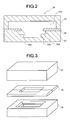
- the metal/ceramic bonding substrate 10 in this preferred embodiment may be produced by, e.g., a method comprising the steps of: preparing a mold 20 shown in FIGS. 2 and 3; arranging the ceramic substrate 12 in the mold 20; injecting a molten metal into the mold 20 so as to contact both sides of the ceramic substrate 12; and thereafter, cooling and solidifying the molten metal to bond the circuit forming metal plate 14 to one side of the ceramic substrate 12 and to bond the radiating metal base plate 16 to the other side thereof.
- the mold 20 comprises lower and upper mold members 22 and 24 which have a substantially rectangular planar shape and which are preferably made of a gas permeable material, such as carbon or a porous metal, and an intermediate mold member 26 of a metal material which is arranged between the lower and upper mold members 22 and 24 and which has a substantially rectangular planar shape.
- a recessed portion serving as a ceramic substrate holding portion 22a which substantially has the same shape and size as those of the ceramic substrate 12.
- the intermediate mold member 26 comprises two pieces for allowing the metal/ceramic bonding substrate 10 to be taken out of the mold, and has such a shape that a through hole serving as a rising portion forming portion 26a, which substantially has the same shape and size as those of the rising portion 16a, is formed in the substantially central portion when the two pieces are aligned with each other.
- the intermediate mold member 26 is preferably formed of a metal material in view of strength, it may be made of the same carbon or porous metal as that of the lower mold member 22.
- a metal base plate forming portion 24a which substantially has the same shape and size as those of a portion of the radiating metal base plate 16 other than the rising portion 16a. Furthermore, a molten metal inlet (not shown) for injecting a molten metal into the mold 20 is formed in the upper mold member 24. In the intermediate mold member 26 and lower mold member 22, a molten metal passage (not shown) extending between the metal base plate forming portion 24a and the metal circuit plate forming portion 22b is formed so as to allow the metal base plate forming portion 24a to be communicated with the metal circuit plate forming portion 22b if the ceramic substrate 12 is housed in the ceramic substrate housing portion 22a.
- the intermediate mold member 26 is arranged on the lower mold member 22, and the upper mold member 24 is arranged thereon to be fixed.
- a molten metal such as molten aluminum
- the molten metal is injected into the metal base plate forming portion 24a to be filled in the metal circuit plate forming portion 22b via the molten metal passage.
- the molten metal is cooled to be solidified to obtain a metal/ceramic bonding substrate 10 wherein the circuit forming metal plate 14 is bonded directly to one side of the ceramic substrate 12 and the radiating metal base plate 16 is bonded directly to the other side thereof, as shown in FIGS. 1A and 1B.
- a resist having a shape of a predetermined circuit pattern is formed on the top face of the circuit forming metal plate 14 to etch the circuit forming metal plate 14 to form a metal circuit plate having the predetermined circuit pattern.
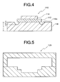
- FIG. 4 shows the second preferred embodiment of a metal/ceramic bonding substrate according to the present invention.
- the metal/ceramic bonding substrate 110 in this preferred embodiment comprises a substantially rectangular flat-plate-shaped ceramic substrate 112, at least one (onlyoneisshowninFIG. 4) substantially rectangular flat-plate-shaped circuit forming metal plate 114 which is bonded to one side of the ceramic substrate 112 and which is smaller than the ceramic substrate 112, and a radiating metal base plate 116 (thickness T) which is bonded to the other side of the ceramic substrate 112 and which has a substantially rectangular planar shape.
- the top face of the metal base plate 116 has a groove portion 116a which extends along the outer periphery of the ceramic substrate 112 and which has a depth d, and the ceramic substrate 112 is bonded to a portion of the top face of the metal base plate 116 surrounded by the groove portion 116b.
- the groove portion 116b is formed so as to straddle the outer periphery of the ceramic substrate 112, so that the area of the bonding surface of the ceramic substrate 112 to the metal base plate 116 is smaller than the area of the ceramic substrate 112.
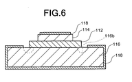
- the metal/ceramic bonding substrate 110 in this preferred embodiment may be produced by, e.g., a method comprising the steps of: preparing a mold 120 shown in FIG. 5, which is the same as the mold 20 used in the first preferred embodiment except that the intermediate mold member 26 is not provided; arranging the ceramic substrate 112 in the mold 120; injecting a molten metal into the mold 120 so as to contact both sides of the ceramic substrate 112; cooling and solidifying the molten metal to bond the circuit forming metal plate 114 to one side of the ceramic substrate 112 and to bond the radiating metal base plate 116 to the other side thereof; forming a resist 118 having a shape of a predetermined pattern on the top face of the circuit forming metal plate 114, and a resist 118 on the substantially entire surface of the metal base plate 116 except for a portion near the peripheral portion of the ceramic substrate 112, as shown in FIG. 6; and thereafter, etching the circuit forming metal plate 114 and the metal base plate 116 to form the groove portion 116b in the
- FIG. 7 shows the third preferred embodiment of a metal/ceramic bonding substrate according to the present invention.
- the metal/ceramic bonding substrate 210 in this preferred embodiment has such a shape that the metal/ceramic bonding substrate 10 in the first preferred embodiment is combined with the metal/ceramic bonding substrate 110 in the second preferred embodiment, and comprises a substantially rectangular flat-plate-shaped ceramic substrate 212, at least one (only one is shown in FIG.
- the metal base plate 216 has a rising portion 216a which rises by a predetermined height h from a surface thereof facing the ceramic substrate 212 in a direction substantially perpendicular thereto and which has a substantially rectangular planar shape smaller than that of the ceramic substrate 212, and a groove portion 216a which extends so as to surround the rising portion 216a and which has a depth d.
- the ceramic substrate 212 is bonded to the top face of the rising portion 216a.
- the metal/ceramic bonding substrate 210 in this preferred embodiment may be produced by, e.g., a method comprising the steps of: using the same mold as the mold 20 shown in FIGS. 2 and 3 in the first preferred embodiment to bond the circuit metal plate 214 to one side of the ceramic substrate 212 and to bond the radiating metal base plate 216 to the other side thereof, by the same method as that in the first preferred embodiment; forming a resist 218 having a shape of a predetermined pattern on the top face of the circuit forming metal plate 214, and a resist 218 on the substantially entire surface of the metal base plate 216 except for a portion near the peripheral portion of the ceramic substrate 212, as shown in FIG. 8; and thereafter, etching the circuit forming metal plate 214 and the metal base plate 216 to form the groove portion 216b in the metal base plate 216.
- FIG. 9 shows the fourth preferred embodiment of a metal/ceramic bonding substrate according to the present invention.
- the metal/ceramic bonding substrate 310 in this preferred embodiment has the same shape as that of the metal/ceramic bonding substrate 10 in the first preferred embodiment, except that the shape of the rising portion 16a is changed to the shape of a rising portion 316a, and comprises a substantially rectangular flat-plate-shaped ceramic substrate 312, at least one (only one is shown in FIG.
- the metal base plate 316 has the rising portion 316a which rises by a predetermined height h from a surface thereof facing the ceramic substrate 312 and which has a substantially rectangular planar shape. To the top face of the rising portion 316a, the ceramic substrate 312 is bonded.
- the angle ⁇ between the bonding surface of the ceramic substrate 312 to the rising portion 316a and the side face of the rising portion 316a is an acute angle ( ⁇ ⁇ 90° ) .
- the metal/ceramic bonding substrate 310 in this preferred embodiment may be produced by, e.g., a method comprising the steps of: preparing a mold 320 shown in FIG. 10; arranging the ceramic substrate 312 in the mold 320; injecting a molten metal into the mold 320 so as to contact both sides of the ceramic substrate 312; and thereafter, cooling and solidifying the molten metal to bond the circuit forming metal plate 314 to one side of the ceramic substrate 312 and to bond the radiating metal base plate 316 to the other side thereof.
- the mold 320 is the same as the mold 20 shown in FIGS. 2 and 3 except for the shape of a through hole serving as a rising portion forming portion 326a of an intermediate mold member 326, and comprises lower and upper mold members 322 and 324 which have a substantially rectangular planar shape and which are preferably made of a gas permeable material, such as carbon or a porous metal, and the intermediate mold member 326 of a metal material or the like which is arranged between the lower and upper mold members 322 and 324 and which has a substantially rectangular planar shape.
- a gas permeable material such as carbon or a porous metal
- a recessed portion serving as a ceramic substrate holding portion 322a which substantially has the same shape and size as those of the ceramic substrate 312.
- a recessed portion serving as a metal circuit plate forming portion 322b which substantially has the same shape and size as those of the circuit forming metal plate 314.
- the intermediate mold member 326 comprises two pieces for allowing the metal/ceramic bonding substrate 310 to be taken out of the mold, and has such a shape that a through hole serving as the rising portion forming portion 326a, which substantially has the same shape and size as those of the rising portion 316a, is formed in the substantially central portion when the two pieces are aligned with each other.
- the intermediate mold member 326 is preferably formed of a metal material in view of strength, it may be made of the same carbon or porous metal as that of the lower mold member 322.
- the upper mold member 324 there is formed a metal base plate forming portion 324a which substantially has the same shape and size as those of a portion of the radiating metal base plate 316 other than the rising portion 316a.
- a molten metal inlet (not shown) for injecting a molten metal into the mold 320 is formed in the upper mold member 324.
- a molten metal passage (not shown) extending between the metal base plate forming portion 324a and the metal circuit plate forming portion 322b is formed so as to allow the metal base plate forming portion 324a to be communicated with the metal circuit plate forming portion 322b if the ceramic substrate 312 is housed in the ceramic substrate housing portion 322a.
- the intermediate mold member 326 is arranged on the lower mold member 322, and the upper mold member 324 is arranged thereon to be fixed.
- a molten metal such as molten aluminum
- the molten metal is injected into the metal base plate forming portion 324a to be filled in the metal circuit plate forming portion 322b via the molten metal passage.
- the molten metal is cooled to be solidified to obtain a metal/ceramic bonding substrate 310 wherein the circuit forming metal plate 314 is bonded directly to one side of the ceramic substrate 312 and the radiating metal base plate 316 is bonded directly to the other side thereof, as shown in FIG. 9.
- a resist having a shape of a predetermined circuit pattern is formed on the top face of the circuit forming metal plate 314 to etch the circuit forming metal plate 314 to form a metal circuit plate having the predetermined circuit pattern.
- FIG. 11 shows the fifth preferred embodiment of a metal/ceramic bonding substrate according to the present invention.
- the metal/ceramic bonding substrate 410 in this preferred embodiment has such a shape that the metal/ceramic bonding substrate 310 in the fourth preferred embodiment is combined with the metal/ceramic bonding substrate 110 in the second preferred embodiment, and comprises a substantially rectangular flat-plate-shaped ceramic substrate 412, at least one (only one is shown in FIG.
- the metal base plate 416 has a rising portion 416a which rises by a predetermined height h from a surface thereof facing the ceramic substrate 412 and which has a substantially rectangular planar shape, and a groove portion 416a which extends so as to surround the rising portion 416a and which has a depth d. To the top face of the rising portion 416a, the ceramic substrate 412 is bonded.
- the angle ⁇ between the bonding surface of the ceramic substrate 412 to the rising portion 416a and the side face of the rising portion 416a is an acute angle ( ⁇ ⁇ 90° ) .
- the metal/ceramic bonding substrate 410 in this preferred embodiment may be produced by, e.g., a method comprising the steps of: using the same mold as the mold 320 shown in FIG. 10 in the first preferred embodiment to bond the circuit metal plate 414 to one side of the ceramic substrate 412 and to bond the radiating metal base plate 416 to the other side thereof, by the same method as that in the fourth preferred embodiment; forming a resist 418 having a shape of a predetermined pattern on the top face of the circuit forming metal plate 414, and a resist 418 on the substantially entire surface of the metal base plate 416 except for a portion near the peripheral portion of the ceramic substrate 412, as shown in FIG. 12; and thereafter, etching the metal base plate 416 to form the groove portion 416b.
- a metal/ceramic bonding substrate according to the present invention may be produced by another method, such as the brazing and soldering method or the direct bonding method. That is, a metal base plate having the same shape as the metal base plate of the metal/ceramic bonding substrate in the above described first through fifth preferred embodiments, and a circuit forming metal plate may be bonded to a ceramic substrate by another method, such as the brazing and soldering method or the direct bonding method.
- the shape of the radiating metal base plate has been the substantially flat plate shape and while the opposite surface (reverse) of the radiating metal base plate to the ceramic substrate has been flat in the above described first through fifth preferred embodiments
- a base plate having fins on its reverse, or a water cooling base plate including a water cooling channel may be used as the radiating metal base plate.
- Such a metal base plate can also obtain the same advantageous effects as those in the above described first through fifth preferred embodiments.
- the single circuit forming metal plate has been illustrated in the above described first through fifth preferred embodiments, the same advantageous effects can be obtained even if a plurality of circuit forming metal plates are used.
- Electrodes were provided on the aluminum plate and aluminum base plate of the metal/ceramic bonding substrate, respectively. Then, the alternating voltage applied between the electrodes in the atmosphere was gradually raised, and a voltage at a leak current of 0.5 mA was measured as a withstand voltage. As a result, the withstand voltage was 2.5 kV or more.
- the withstand voltage of this metal/ceramic bonding substrate was measured by the same method as that in Example 1, the withstand voltage was 2.5 kV or more.
- a crack having a length of 1 mm was produced in the aluminum base plate under the aluminum nitride substrate after the same heat cycles as those in Example 1 were repeatedly carried out three thousands times, and a crack having a length of 3 mm was produced therein after the same heat cycles were repeatedly carried out five thousands times.
- resists were formed for etching the aluminum base plate to form a groove portion having a depth of 0.5 mm to produce a metal/ceramic bonding substrate having a shape similar to that of the metal/ceramic bonding substrate in the third preferred embodiment.
- the withstand voltage of this metal/ceramic bonding substrate was measured by the same method as that in Example 1, the withstand voltage was 2.5 kV or more.
- no crack was observed on the aluminum base plate under the aluminum nitride substrate after the same heat cycles as those in Example 1 were repeatedly carried out three thousands times, and a crack having a length of 1 mm was produced therein after the same heat cycles were repeatedly carried out five thousands times.
- the withstand voltage of this metal/ceramic bonding substrate was measured by the same method as that in Example 1, the withstand voltage was 2.5 kV or more.
- no crack was observed on the aluminum base plate under the aluminum nitride substrate after the same heat cycles as those in Example 1 were repeatedly carried out three thousands times, and a crack having a length of 1 mm was produced therein after the same heat cycles were repeatedly carried out five thousands times.
- resists were formed for etching the aluminum base plate to form a groove portion having a depth of 0.5 mm to produce a metal/ceramic bonding substrate having a shape similar to that of the metal/ceramic bonding substrate in the fifth preferred embodiment.
- the withstand voltage of this metal/ceramic bonding substrate was measured by the same method as that in Example 1, the withstand voltage was 2.5 kV or more.
- no crack was observed on the aluminum base plate under the aluminum nitride substrate after the same heat cycles as those in Example 1 were repeatedly carried out three thousands times, and no crack was also observed thereon after the same heat cycles were repeatedly carried out five thousands times.
- Example 3 By the same method as that in Example 3, except that the thickness of the aluminum nitride substrate was 0.3 mm, a metal/ceramic bonding substrate having a shape similar to that of the metal/ceramic bonding substrate in the third preferred embodiment was produced. After the withstand voltage of this metal/ceramic bonding substrate was measured by the same method as that in Example 1, the withstand voltage was 2.5 kV or more. In addition, no crack was observed on the aluminum base plate under the aluminum nitride substrate after the same heat cycles as those in Example 1 were repeatedly carried out three thousands times, and a crack having a length of 1 mm was produced therein after the same heat cycles were repeatedly carried out five thousands times.
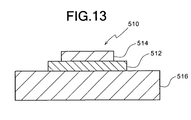
- a mold shown in FIG. 5 was used for bonding three aluminum plates 514 (only one aluminum plate 514 is shown in FIG. 13) having a thickness of 0. 4 mm to one side of an aluminum nitride substrate 512 having a size of 36 mm x 40 mm x 0.635 mm, and an aluminum base plate 516 having a thickness of 5 mm to the other side thereof, as shown in FIG. 13.
- the withstand voltage of the metal/ceramic bonding substrate thus obtained was measured by the same method as that in Example 1, the withstand voltage was less than 2.0 kV.
- a crack having a length of 3 mm was produced in the aluminum base plate under the aluminum nitride substrate after the same heat cycles as those in Example 1 were repeatedly carried out three thousands times.
- the withstand voltage was only less than 2.0 kV in Comparative Example, whereas the withstand voltage was 2.5 kV or more in Examples 1 through 6.
- the crack having the length of 3 mm was produced in the aluminum base plate under the aluminum nitride substrate after 3000 heat cycles.
- the length of the crack was only 1 mm after 3000 heat cycles, and in Examples 3 through 6, no crack was observed after 3000 heat cycles.
- the length of the crack did not reach 3 mm unless the heat cycles were repeatedly carried out five thousands times.
- the length of the crack was only 1 mm after 5000 heat cycles, and in Example 5, no crack was observed after 5000 heat cycles.
Landscapes
- Structure Of Printed Boards (AREA)
- Ceramic Products (AREA)
- Cooling Or The Like Of Semiconductors Or Solid State Devices (AREA)
- ing And Chemical Polishing (AREA)
- Manufacturing Of Printed Wiring (AREA)
- Insulated Metal Substrates For Printed Circuits (AREA)
Applications Claiming Priority (2)
| Application Number | Priority Date | Filing Date | Title |
|---|---|---|---|
| JP2003351936A JP4496404B2 (ja) | 2003-10-10 | 2003-10-10 | 金属−セラミックス接合基板およびその製造方法 |
| JP2003351936 | 2003-10-10 |
Publications (3)
| Publication Number | Publication Date |
|---|---|
| EP1523037A2 true EP1523037A2 (fr) | 2005-04-13 |
| EP1523037A3 EP1523037A3 (fr) | 2010-03-31 |
| EP1523037B1 EP1523037B1 (fr) | 2020-03-18 |
Family
ID=34309281
Family Applications (1)
| Application Number | Title | Priority Date | Filing Date |
|---|---|---|---|
| EP04024192.9A Expired - Lifetime EP1523037B1 (fr) | 2003-10-10 | 2004-10-11 | Procédé de fabrication d'un substrat composite métal/céramique |
Country Status (3)
| Country | Link |
|---|---|
| US (1) | US7189449B2 (fr) |
| EP (1) | EP1523037B1 (fr) |
| JP (1) | JP4496404B2 (fr) |
Cited By (5)
| Publication number | Priority date | Publication date | Assignee | Title |
|---|---|---|---|---|
| EP2109138A4 (fr) * | 2006-12-26 | 2012-02-22 | Kyocera Corp | Substrat de dissipation de chaleur et dispositif electronique utilisant un tel substrat |
| EP2833399A4 (fr) * | 2012-03-30 | 2015-12-30 | Mitsubishi Materials Corp | Substrat de module de puissance, substrat de module de puissance muni de dissipateur thermique, et module de puissance |
| WO2022018063A1 (fr) * | 2020-07-21 | 2022-01-27 | Rogers Germany Gmbh | Module de puissance et procédé de fabrication d'un module de puissance |
| DE102023200812A1 (de) * | 2023-02-01 | 2024-08-01 | Volkswagen Aktiengesellschaft | Elektronisches Bauteil, insbesondere Pulswechselrichter sowie Fahrzeug mit einem elektronischen Bauteil |
| EP3584828B1 (fr) * | 2016-12-22 | 2024-10-30 | Rogers Germany GmbH | Substrat porteur pour composants électriques et procédé de fabrication d'un substrat porteur |
Families Citing this family (9)
| Publication number | Priority date | Publication date | Assignee | Title |
|---|---|---|---|---|
| JP4543279B2 (ja) * | 2004-03-31 | 2010-09-15 | Dowaメタルテック株式会社 | アルミニウム接合部材の製造方法 |
| JP2007294891A (ja) * | 2006-03-30 | 2007-11-08 | Dowa Metaltech Kk | 放熱器 |
| JP4965305B2 (ja) * | 2006-03-31 | 2012-07-04 | Dowaメタルテック株式会社 | 金属−セラミックス接合基板の製造方法 |
| US7923200B2 (en) * | 2007-04-09 | 2011-04-12 | Az Electronic Materials Usa Corp. | Composition for coating over a photoresist pattern comprising a lactam |
| US7745077B2 (en) * | 2008-06-18 | 2010-06-29 | Az Electronic Materials Usa Corp. | Composition for coating over a photoresist pattern |
| US7898807B2 (en) * | 2009-03-09 | 2011-03-01 | General Electric Company | Methods for making millichannel substrate, and cooling device and apparatus using the substrate |
| CN103338613B (zh) * | 2012-10-15 | 2016-05-11 | 东莞生益电子有限公司 | 具有非对称散热结构的电子设备 |
| JP7267030B2 (ja) * | 2019-02-20 | 2023-05-01 | Dowaメタルテック株式会社 | 金属-セラミックス接合基板およびその製造方法 |
| JP7806561B2 (ja) * | 2022-03-11 | 2026-01-27 | 三菱マテリアル株式会社 | 絶縁回路基板 |
Citations (2)
| Publication number | Priority date | Publication date | Assignee | Title |
|---|---|---|---|---|
| US5692720A (en) | 1996-01-05 | 1997-12-02 | Griggs; George J. | Anchoring device for umbrellas |
| DE19959248A1 (de) | 1999-12-08 | 2001-06-28 | Daimler Chrysler Ag | Isolationsverbesserung bei Hochleistungs-Halbleitermodulen |
Family Cites Families (20)
| Publication number | Priority date | Publication date | Assignee | Title |
|---|---|---|---|---|
| JPS52117556A (en) * | 1976-03-30 | 1977-10-03 | Toshiba Corp | Photo mask and its manufacturing method |
| JPS5952853A (ja) * | 1982-09-20 | 1984-03-27 | Hitachi Ltd | 半導体装置 |
| US5570502A (en) * | 1991-04-08 | 1996-11-05 | Aluminum Company Of America | Fabricating metal matrix composites containing electrical insulators |
| US5213877A (en) * | 1991-05-02 | 1993-05-25 | Mitsubishi Materials Corporation | Ceramic substrate used for fabricating electric or electronic circuit |
| US5602720A (en) * | 1993-06-25 | 1997-02-11 | Sumitomo Electric Industries, Ltd. | Mounting structure for semiconductor device having low thermal resistance |
| US5965193A (en) * | 1994-04-11 | 1999-10-12 | Dowa Mining Co., Ltd. | Process for preparing a ceramic electronic circuit board and process for preparing aluminum or aluminum alloy bonded ceramic material |
| JP2918191B2 (ja) * | 1994-04-11 | 1999-07-12 | 同和鉱業株式会社 | 金属−セラミックス複合部材の製造方法 |
| JPH0883864A (ja) * | 1994-09-13 | 1996-03-26 | Meidensha Corp | 電力用半導体装置 |
| JP4077888B2 (ja) * | 1995-07-21 | 2008-04-23 | 株式会社東芝 | セラミックス回路基板 |
| JPH09289266A (ja) * | 1996-04-19 | 1997-11-04 | Dowa Mining Co Ltd | Al−セラミックス複合基板 |
| JP3837680B2 (ja) * | 1996-10-24 | 2006-10-25 | 同和鉱業株式会社 | 金属−セラミックス複合基板製造用鋳型 |
| JPH10189803A (ja) * | 1996-12-27 | 1998-07-21 | Nippon Inter Electronics Corp | 放熱板への絶縁基板取付構造 |
| US6294244B1 (en) * | 1997-12-22 | 2001-09-25 | Kyocera Corporation | Wiring board having excellent heat-radiating property |
| JPH11265976A (ja) * | 1998-03-18 | 1999-09-28 | Mitsubishi Electric Corp | パワー半導体モジュールおよびその製造方法 |
| DE60037069T2 (de) * | 1999-05-28 | 2008-09-11 | Denki Kagaku Kogyo K.K. | Schaltung mit Substrat |
| JP4756200B2 (ja) | 2000-09-04 | 2011-08-24 | Dowaメタルテック株式会社 | 金属セラミックス回路基板 |
| JP2003060282A (ja) * | 2001-08-20 | 2003-02-28 | Toshiba Corp | サブマウント材 |
| JP4867042B2 (ja) * | 2001-08-29 | 2012-02-01 | Dowaメタルテック株式会社 | 金属と金属またはセラミックスとの接合方法 |
| JP2003100938A (ja) * | 2001-09-26 | 2003-04-04 | Mitsubishi Electric Corp | 半導体装置 |
| EP1324386B1 (fr) * | 2001-12-24 | 2011-06-15 | ABB Research Ltd. | Module semi-conductreur et méthode de fabrication d'un module semi-conducteur |
-
2003
- 2003-10-10 JP JP2003351936A patent/JP4496404B2/ja not_active Expired - Lifetime
-
2004
- 2004-10-11 EP EP04024192.9A patent/EP1523037B1/fr not_active Expired - Lifetime
- 2004-10-12 US US10/964,426 patent/US7189449B2/en not_active Expired - Lifetime
Patent Citations (2)
| Publication number | Priority date | Publication date | Assignee | Title |
|---|---|---|---|---|
| US5692720A (en) | 1996-01-05 | 1997-12-02 | Griggs; George J. | Anchoring device for umbrellas |
| DE19959248A1 (de) | 1999-12-08 | 2001-06-28 | Daimler Chrysler Ag | Isolationsverbesserung bei Hochleistungs-Halbleitermodulen |
Cited By (6)
| Publication number | Priority date | Publication date | Assignee | Title |
|---|---|---|---|---|
| EP2109138A4 (fr) * | 2006-12-26 | 2012-02-22 | Kyocera Corp | Substrat de dissipation de chaleur et dispositif electronique utilisant un tel substrat |
| EP2833399A4 (fr) * | 2012-03-30 | 2015-12-30 | Mitsubishi Materials Corp | Substrat de module de puissance, substrat de module de puissance muni de dissipateur thermique, et module de puissance |
| US9480144B2 (en) | 2012-03-30 | 2016-10-25 | Mitsubishi Materials Corporation | Power module substrate, power module substrate with heat sink, and power module |
| EP3584828B1 (fr) * | 2016-12-22 | 2024-10-30 | Rogers Germany GmbH | Substrat porteur pour composants électriques et procédé de fabrication d'un substrat porteur |
| WO2022018063A1 (fr) * | 2020-07-21 | 2022-01-27 | Rogers Germany Gmbh | Module de puissance et procédé de fabrication d'un module de puissance |
| DE102023200812A1 (de) * | 2023-02-01 | 2024-08-01 | Volkswagen Aktiengesellschaft | Elektronisches Bauteil, insbesondere Pulswechselrichter sowie Fahrzeug mit einem elektronischen Bauteil |
Also Published As
| Publication number | Publication date |
|---|---|
| EP1523037A3 (fr) | 2010-03-31 |
| US7189449B2 (en) | 2007-03-13 |
| JP2005116934A (ja) | 2005-04-28 |
| EP1523037B1 (fr) | 2020-03-18 |
| US20050079329A1 (en) | 2005-04-14 |
| JP4496404B2 (ja) | 2010-07-07 |
Similar Documents
| Publication | Publication Date | Title |
|---|---|---|
| US7189449B2 (en) | Metal/ceramic bonding substrate and method for producing same | |
| US11162745B2 (en) | Heat radiating plate and method for producing same | |
| EP1345480B1 (fr) | Panneau à circuit céramique | |
| US8039757B2 (en) | Electronic part mounting substrate and method for producing same | |
| JP5837754B2 (ja) | 金属−セラミックス接合基板およびその製造方法 | |
| US7122243B2 (en) | Metal/ceramic bonding substrate and method for producing same | |
| US20230294213A1 (en) | Method for producing a metal-ceramic substrate, and metal-ceramic substrate produced using a method of this type | |
| JP4722415B2 (ja) | 半導体装置およびその製造方法 | |
| JP5619437B2 (ja) | 金属−セラミックス接合基板の製造方法 | |
| KR102730548B1 (ko) | 양면 냉각형 파워모듈 및 그 제조 방법 | |
| US10529643B2 (en) | Semiconductor device and method of manufacturing the same | |
| US20050060887A1 (en) | Method for producing metal/ceramic bonding circuit board | |
| JP4565249B2 (ja) | 金属−セラミックス接合基板およびその製造方法 | |
| US20050072547A1 (en) | Aluminum/ceramic bonding substrate and method for producing same | |
| EP0646958A2 (fr) | Boîtier et module pour semi-conducteur et procédé de fabrication | |
| US20260047451A1 (en) | Semiconductor package, power electronic system and method for coupling a semiconductor package to a heatsink | |
| JP7601261B2 (ja) | 半導体装置及びその製造方法 | |
| JP7796512B2 (ja) | 金属-セラミックス接合基板およびその製造方法 | |
| JP2020132477A (ja) | 金属−セラミックス接合基板およびその製造方法 |
Legal Events
| Date | Code | Title | Description |
|---|---|---|---|
| PUAI | Public reference made under article 153(3) epc to a published international application that has entered the european phase |
Free format text: ORIGINAL CODE: 0009012 |
|
| AK | Designated contracting states |
Kind code of ref document: A2 Designated state(s): AT BE BG CH CY CZ DE DK EE ES FI FR GB GR HU IE IT LI LU MC NL PL PT RO SE SI SK TR |
|
| AX | Request for extension of the european patent |
Extension state: AL HR LT LV MK |
|
| RAP1 | Party data changed (applicant data changed or rights of an application transferred) |
Owner name: DOWA HOLDINGS CO., LTD. |
|
| RAP1 | Party data changed (applicant data changed or rights of an application transferred) |
Owner name: DOWA METALTECH CO., LTD. |
|
| PUAL | Search report despatched |
Free format text: ORIGINAL CODE: 0009013 |
|
| AK | Designated contracting states |
Kind code of ref document: A3 Designated state(s): AT BE BG CH CY CZ DE DK EE ES FI FR GB GR HU IE IT LI LU MC NL PL PT RO SE SI SK TR |
|
| AX | Request for extension of the european patent |
Extension state: AL HR LT LV MK |
|
| 17P | Request for examination filed |
Effective date: 20100810 |
|
| AKX | Designation fees paid |
Designated state(s): CH DE FR GB LI |
|
| 17Q | First examination report despatched |
Effective date: 20110414 |
|
| GRAP | Despatch of communication of intention to grant a patent |
Free format text: ORIGINAL CODE: EPIDOSNIGR1 |
|
| INTG | Intention to grant announced |
Effective date: 20190930 |
|
| GRAS | Grant fee paid |
Free format text: ORIGINAL CODE: EPIDOSNIGR3 |
|
| GRAA | (expected) grant |
Free format text: ORIGINAL CODE: 0009210 |
|
| REG | Reference to a national code |
Ref country code: DE Ref legal event code: R081 Ref document number: 602004054559 Country of ref document: DE Owner name: DOWA METALTECH CO., LTD., JP Free format text: FORMER OWNER: DOWA MINING CO., LTD., TOKIO/TOKYO, JP |
|
| AK | Designated contracting states |
Kind code of ref document: B1 Designated state(s): CH DE FR GB LI |
|
| REG | Reference to a national code |
Ref country code: GB Ref legal event code: FG4D |
|
| REG | Reference to a national code |
Ref country code: DE Ref legal event code: R096 Ref document number: 602004054559 Country of ref document: DE |
|
| REG | Reference to a national code |
Ref country code: CH Ref legal event code: NV Representative=s name: INTELLECTUAL PROPERTY SERVICES GMBH, CH |
|
| REG | Reference to a national code |
Ref country code: DE Ref legal event code: R097 Ref document number: 602004054559 Country of ref document: DE |
|
| PLBE | No opposition filed within time limit |
Free format text: ORIGINAL CODE: 0009261 |
|
| STAA | Information on the status of an ep patent application or granted ep patent |
Free format text: STATUS: NO OPPOSITION FILED WITHIN TIME LIMIT |
|
| 26N | No opposition filed |
Effective date: 20201221 |
|
| PGFP | Annual fee paid to national office [announced via postgrant information from national office to epo] |
Ref country code: GB Payment date: 20230831 Year of fee payment: 20 |
|
| PGFP | Annual fee paid to national office [announced via postgrant information from national office to epo] |
Ref country code: FR Payment date: 20230911 Year of fee payment: 20 |
|
| PGFP | Annual fee paid to national office [announced via postgrant information from national office to epo] |
Ref country code: DE Payment date: 20230830 Year of fee payment: 20 Ref country code: CH Payment date: 20231102 Year of fee payment: 20 |
|
| REG | Reference to a national code |
Ref country code: DE Ref legal event code: R071 Ref document number: 602004054559 Country of ref document: DE |
|
| REG | Reference to a national code |
Ref country code: CH Ref legal event code: PL |
|
| REG | Reference to a national code |
Ref country code: GB Ref legal event code: PE20 Expiry date: 20241010 |
|
| PG25 | Lapsed in a contracting state [announced via postgrant information from national office to epo] |
Ref country code: GB Free format text: LAPSE BECAUSE OF EXPIRATION OF PROTECTION Effective date: 20241010 |
|
| PG25 | Lapsed in a contracting state [announced via postgrant information from national office to epo] |
Ref country code: GB Free format text: LAPSE BECAUSE OF EXPIRATION OF PROTECTION Effective date: 20241010 |