EP1523096A2 - Résonateur à couche à ondes acoustiques de volume et procéde de fabrication dudit résonateur - Google Patents
Résonateur à couche à ondes acoustiques de volume et procéde de fabrication dudit résonateur Download PDFInfo
- Publication number
- EP1523096A2 EP1523096A2 EP04255089A EP04255089A EP1523096A2 EP 1523096 A2 EP1523096 A2 EP 1523096A2 EP 04255089 A EP04255089 A EP 04255089A EP 04255089 A EP04255089 A EP 04255089A EP 1523096 A2 EP1523096 A2 EP 1523096A2
- Authority
- EP
- European Patent Office
- Prior art keywords
- membrane
- vapor
- deposited
- substrate
- manufacturing
- Prior art date
- Legal status (The legal status is an assumption and is not a legal conclusion. Google has not performed a legal analysis and makes no representation as to the accuracy of the status listed.)
- Granted
Links
Images



Classifications
-
- H—ELECTRICITY
- H03—ELECTRONIC CIRCUITRY
- H03H—IMPEDANCE NETWORKS, e.g. RESONANT CIRCUITS; RESONATORS
- H03H9/00—Networks comprising electromechanical or electro-acoustic elements; Electromechanical resonators
- H03H9/24—Constructional features of resonators of material which is not piezoelectric, electrostrictive, or magnetostrictive
-
- H—ELECTRICITY
- H03—ELECTRONIC CIRCUITRY
- H03H—IMPEDANCE NETWORKS, e.g. RESONANT CIRCUITS; RESONATORS
- H03H9/00—Networks comprising electromechanical or electro-acoustic elements; Electromechanical resonators
- H03H9/15—Constructional features of resonators consisting of piezoelectric or electrostrictive material
- H03H9/17—Constructional features of resonators consisting of piezoelectric or electrostrictive material having a single resonator
- H03H9/171—Constructional features of resonators consisting of piezoelectric or electrostrictive material having a single resonator implemented with thin-film techniques, i.e. of the film bulk acoustic resonator [FBAR] type
- H03H9/172—Means for mounting on a substrate, i.e. means constituting the material interface confining the waves to a volume
- H03H9/173—Air-gaps
-
- H—ELECTRICITY
- H03—ELECTRONIC CIRCUITRY
- H03H—IMPEDANCE NETWORKS, e.g. RESONANT CIRCUITS; RESONATORS
- H03H3/00—Apparatus or processes specially adapted for the manufacture of impedance networks, resonating circuits, resonators
- H03H3/007—Apparatus or processes specially adapted for the manufacture of impedance networks, resonating circuits, resonators for the manufacture of electromechanical resonators or networks
- H03H3/02—Apparatus or processes specially adapted for the manufacture of impedance networks, resonating circuits, resonators for the manufacture of electromechanical resonators or networks for the manufacture of piezoelectric or electrostrictive resonators or networks
-
- H—ELECTRICITY
- H03—ELECTRONIC CIRCUITRY
- H03H—IMPEDANCE NETWORKS, e.g. RESONANT CIRCUITS; RESONATORS
- H03H9/00—Networks comprising electromechanical or electro-acoustic elements; Electromechanical resonators
- H03H9/02—Details
- H03H9/02007—Details of bulk acoustic wave devices
- H03H9/02086—Means for compensation or elimination of undesirable effects
- H03H9/02133—Means for compensation or elimination of undesirable effects of stress
-
- H—ELECTRICITY
- H03—ELECTRONIC CIRCUITRY
- H03H—IMPEDANCE NETWORKS, e.g. RESONANT CIRCUITS; RESONATORS
- H03H3/00—Apparatus or processes specially adapted for the manufacture of impedance networks, resonating circuits, resonators
- H03H3/007—Apparatus or processes specially adapted for the manufacture of impedance networks, resonating circuits, resonators for the manufacture of electromechanical resonators or networks
- H03H3/02—Apparatus or processes specially adapted for the manufacture of impedance networks, resonating circuits, resonators for the manufacture of electromechanical resonators or networks for the manufacture of piezoelectric or electrostrictive resonators or networks
- H03H2003/021—Apparatus or processes specially adapted for the manufacture of impedance networks, resonating circuits, resonators for the manufacture of electromechanical resonators or networks for the manufacture of piezoelectric or electrostrictive resonators or networks the resonators or networks being of the air-gap type
-
- Y—GENERAL TAGGING OF NEW TECHNOLOGICAL DEVELOPMENTS; GENERAL TAGGING OF CROSS-SECTIONAL TECHNOLOGIES SPANNING OVER SEVERAL SECTIONS OF THE IPC; TECHNICAL SUBJECTS COVERED BY FORMER USPC CROSS-REFERENCE ART COLLECTIONS [XRACs] AND DIGESTS
- Y10—TECHNICAL SUBJECTS COVERED BY FORMER USPC
- Y10T—TECHNICAL SUBJECTS COVERED BY FORMER US CLASSIFICATION
- Y10T29/00—Metal working
- Y10T29/42—Piezoelectric device making
-
- Y—GENERAL TAGGING OF NEW TECHNOLOGICAL DEVELOPMENTS; GENERAL TAGGING OF CROSS-SECTIONAL TECHNOLOGIES SPANNING OVER SEVERAL SECTIONS OF THE IPC; TECHNICAL SUBJECTS COVERED BY FORMER USPC CROSS-REFERENCE ART COLLECTIONS [XRACs] AND DIGESTS
- Y10—TECHNICAL SUBJECTS COVERED BY FORMER USPC
- Y10T—TECHNICAL SUBJECTS COVERED BY FORMER US CLASSIFICATION
- Y10T29/00—Metal working
- Y10T29/49—Method of mechanical manufacture
- Y10T29/49002—Electrical device making
- Y10T29/49117—Conductor or circuit manufacturing
- Y10T29/49124—On flat or curved insulated base, e.g., printed circuit, etc.
- Y10T29/49126—Assembling bases
-
- Y—GENERAL TAGGING OF NEW TECHNOLOGICAL DEVELOPMENTS; GENERAL TAGGING OF CROSS-SECTIONAL TECHNOLOGIES SPANNING OVER SEVERAL SECTIONS OF THE IPC; TECHNICAL SUBJECTS COVERED BY FORMER USPC CROSS-REFERENCE ART COLLECTIONS [XRACs] AND DIGESTS
- Y10—TECHNICAL SUBJECTS COVERED BY FORMER USPC
- Y10T—TECHNICAL SUBJECTS COVERED BY FORMER US CLASSIFICATION
- Y10T29/00—Metal working
- Y10T29/49—Method of mechanical manufacture
- Y10T29/49002—Electrical device making
- Y10T29/49117—Conductor or circuit manufacturing
- Y10T29/49124—On flat or curved insulated base, e.g., printed circuit, etc.
- Y10T29/49128—Assembling formed circuit to base
-
- Y—GENERAL TAGGING OF NEW TECHNOLOGICAL DEVELOPMENTS; GENERAL TAGGING OF CROSS-SECTIONAL TECHNOLOGIES SPANNING OVER SEVERAL SECTIONS OF THE IPC; TECHNICAL SUBJECTS COVERED BY FORMER USPC CROSS-REFERENCE ART COLLECTIONS [XRACs] AND DIGESTS
- Y10—TECHNICAL SUBJECTS COVERED BY FORMER USPC
- Y10T—TECHNICAL SUBJECTS COVERED BY FORMER US CLASSIFICATION
- Y10T29/00—Metal working
- Y10T29/49—Method of mechanical manufacture
- Y10T29/49002—Electrical device making
- Y10T29/49117—Conductor or circuit manufacturing
- Y10T29/49124—On flat or curved insulated base, e.g., printed circuit, etc.
- Y10T29/4913—Assembling to base an electrical component, e.g., capacitor, etc.
-
- Y—GENERAL TAGGING OF NEW TECHNOLOGICAL DEVELOPMENTS; GENERAL TAGGING OF CROSS-SECTIONAL TECHNOLOGIES SPANNING OVER SEVERAL SECTIONS OF THE IPC; TECHNICAL SUBJECTS COVERED BY FORMER USPC CROSS-REFERENCE ART COLLECTIONS [XRACs] AND DIGESTS
- Y10—TECHNICAL SUBJECTS COVERED BY FORMER USPC
- Y10T—TECHNICAL SUBJECTS COVERED BY FORMER US CLASSIFICATION
- Y10T29/00—Metal working
- Y10T29/49—Method of mechanical manufacture
- Y10T29/49002—Electrical device making
- Y10T29/49117—Conductor or circuit manufacturing
- Y10T29/49124—On flat or curved insulated base, e.g., printed circuit, etc.
- Y10T29/4913—Assembling to base an electrical component, e.g., capacitor, etc.
- Y10T29/49133—Assembling to base an electrical component, e.g., capacitor, etc. with component orienting
- Y10T29/49135—Assembling to base an electrical component, e.g., capacitor, etc. with component orienting and shaping, e.g., cutting or bending, etc.
-
- Y—GENERAL TAGGING OF NEW TECHNOLOGICAL DEVELOPMENTS; GENERAL TAGGING OF CROSS-SECTIONAL TECHNOLOGIES SPANNING OVER SEVERAL SECTIONS OF THE IPC; TECHNICAL SUBJECTS COVERED BY FORMER USPC CROSS-REFERENCE ART COLLECTIONS [XRACs] AND DIGESTS
- Y10—TECHNICAL SUBJECTS COVERED BY FORMER USPC
- Y10T—TECHNICAL SUBJECTS COVERED BY FORMER US CLASSIFICATION
- Y10T29/00—Metal working
- Y10T29/49—Method of mechanical manufacture
- Y10T29/49002—Electrical device making
- Y10T29/49117—Conductor or circuit manufacturing
- Y10T29/49124—On flat or curved insulated base, e.g., printed circuit, etc.
- Y10T29/49155—Manufacturing circuit on or in base
Definitions
- the present invention relates to an acoustic filter used in wireless communication devices, and more particularly, to a film bulk acoustic resonator (hereinafter, referred to as "FBAR") which implements a high pass filter for passing only a specified high frequency component, and a method for manufacturing the same.
- FBAR film bulk acoustic resonator
- FBAR FBAR
- PCS personal communication system
- DCS digital cordless system
- an FBAR element comprises a laminated resonance part created by a first electrode, a piezoelectric layer and a second electrode vapor-deposited in the above order on a substrate.
- the FBAR is operated as follows. Electric energy is applied to an electrode, and an electric field which temporally changes is induced in the piezoelectric layer. Then, the electric field causes a bulk acoustic wave in the piezoelectric layer in the same direction as a vibration in the laminated resonance part, and generates the resonance.
- the FBAR element includes, as shown in FIGS. 1A through 1D, a Bragg reflector-type FBAR and an air gap-type FBAR.
- the Bragg reflector-type FBAR of FIG. 1A is formed by vapor-depositing in order of a reflection layer 11, a lower electrode 12, a piezoelectric layer 13, and an upper electrode 14.
- the reflection layer 11 is formed by vapor-depositing on a substrate 10 materials having a large difference of elastic impedance in an alternate manner.
- the Bragg reflector-type FBAR has a firm structure without a stress from bending, however, it is hard to form the reflection layer of at least 4 layers in precise thickness for total reflection. Additionally, a significant amount of manufacturing time and a large cost are required.
- the air gap-type FBAR uses an air gap instead of the reflection layer to separate the substrate from the resonance part, and is divided into several types according to the manufacturing method used. Different types of air gap-type FBAR elements are illustrated in FIGS. 1B through 1D.
- the FBAR element in FIG. 1B is a bulk micro-machining FBAR fabricated in a manner that a membrane 21 is formed by SiO 2 , for example, on the substrate 20, a cavity part 23 is defined by the anisotropic etching of a rear side of the substrate 20, and the acoustic resonator 22 is formed on the membrane 21.
- An FBAR element thus structured is not practical due to its very weak structure and a low recovery rate.
- the FBAR element in FIG. 1C is a surface micro-machining FBAR fabricated as follows.
- a sacrifice layer (not shown) is formed on the substrate 30, and an insulation membrane 32 is formed on the sacrifice layer and the substrate 30.
- a first electrode 33, a piezoelectric layer 34 and a second electrode 35 are vapor-deposited in order, and finally, the sacrifice layer is removed to form an air gap 31.
- a via hole (not shown) is formed to connect the exterior of the element to the sacrifice layer inside the element, and an etchant is injected through the via hole to remove the sacrifice layer. Consequently, the air gap 31 is formed.
- the sacrifice layer needs to be slanted, which causes a weak structure due to a high remaining stress of the membrane.
- the FBAR element of FIG. 1D is fabricated in the following manner.
- a cavity part 45 is defined by etching a substrate 40 using a photo-resist membrane, and a sacrifice layer (not shown) is vapor-deposited on the cavity part 45.
- a membrane 41, a first electrode 42, a piezoelectric layer 43, and a second electrode 44 are vapor-deposited in order on the sacrifice layer and the substrate 40.
- an air gap 45 is formed by etching the sacrifice layer.
- a wet etching and a dry etching are employed in forming the air gap 45.
- the etching is accomplished by a plasmatic gas. At this time, physical impact can be caused by an ion and a molecule, and the membrane 41 or the substrate 40 can be deteriorated by high temperature.
- a film bulk acoustic resonator comprising: a substrate; a protection layer vapor-deposited on the substrate; a membrane vapor-deposited on the protection layer and at a predetermined distance from an upper side of the substrate; and a laminated resonance part vapor-deposited on the membrane.
- the protection layer is preferably vapor-deposited on both sides of the substrate. except for a predetermined part.
- the predetermined part preferably defines an air gap.
- the laminated resonance part preferably comprises a lower electrode vapor-deposited on the membrane, a piezoelectric layer vapor-deposited on the lower electrode, and an upper electrode vapor-deposited on the piezoelectric layer.
- the membrane may be a single layer of nitride, or multiple layers in which a nitride membrane, an oxidized membrane and the nitride membrane are sequentially vapor-deposited.
- a method for manufacturing a film bulk acoustic resonator comprising vapor-depositing a membrane on a substrate;forming protection layers on both sides of the membrane; vapor-depositing a laminated resonance part on the membrane, and forming an air gap by removing a part of the substrate disposed between the protection layers.
- the protection layer may be formed by a LOCOS process, and the air gap may be formed by dry etching or wet etching.
- the present invention thus provides a film bulk acoustic resonator having an improved degree of integration and a simple structure, wherein an air gap is formed by using a part of a substrate oxidized by LOCOS process for an etching stop layer, and etching a part of the other substrate, and the method for manufacturing the same.
- the FBAR according to the present invention comprises a substrate 100 including an air gap 100a, a membrane 150 vapor-deposited on the air gap 100a to be at a predetermined distance from the substrate 100, and a laminated resonance part 200 vapor-deposited on the membrane 150.
- protection layers 110a and 110b are vapor-deposited.
- the protection layers 110a and 110b are formed by a localized oxidation isolation method (LOCO) process which oxidizes the substrate 100 using a mask, and functions as an etching stop layer in an etching process for forming the air gap 100a, which will be described later.
- LOCO localized oxidation isolation method
- the certain part on the top of the substrate 100, wherein the protection layers 110a and 110b are not vapor-deposited, is a part corresponding to the air gap 100a.
- the air gap 100a isolates the substrate 100 and the laminated resonance part 200 from each other.
- a silicon wafer is generally used for the substrate 100.
- the membrane 150 is vapor-deposited on an upper part of the air gap 100a vapor-deposited between the protection layers 110a and 110b which are on the substrate 100.
- the membrane 150 supports the laminated resonance part 200, and functions as an oxidation stop layer during the LOCOS process.
- the membrane 150 may be formed of a single layer of nitride.
- the membrane 150 can be formed of a multiple layer in which a nitride membrane, an oxidized membrane and the nitride membrane are alternately vapor-deposited. Therefore, the membrane 150 can be realized in a simple structure and without stress.
- the laminated resonance part 200 comprises a lower electrode 210, a piezoelectric layer 220, and an upper electrode 230.
- the lower electrode 210 is vapor-deposited on the membrane 150 and one of the protection layer 110a, and the piezoelectric layer 220 is vapor-deposited on the lower electrode 210 and the other protection layer 110b.
- the upper electrode 230 is vapor-deposited on the piezoelectric layer 220.
- the lower and the upper electrodes 210 and 230 use a general electric conductor such as a metal, to apply an electric field to the piezoelectric layer 220.
- the piezoelectric layer 220 causes a piezoelectric effect when being applied with the electric field, and therefore generates an acoustic wave.
- AIN, ZnO, or other material can be used for the piezoelectric material.
- the acoustic wave generated at the piezoelectric layer 220 is reflected by the air gap 100a, and the resonance effect is enlarged.
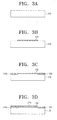
- FIGS. 3A to 3C showing respective processes of manufacturing the FBAR.
- FIGS. 3A to 3C show the process of vapor-depositing the membrane 150 and the protection layers 110a and 110b on the substrate 110 using the LOCOS process.
- the LOCOS process refers to an oxidation process selectively performed with respect to the silicon.
- an oxidation stop layer such as nitride, which can effectively prevent oxygen or vapor from diffusing, and the other area not provided.
- a thick oxidation membrane is formed on the area wherein the oxidation stop layer is not formed, using a difference in growth rate of thermal oxidization membrane of the two areas.
- the membrane 150 may be formed with a single layer of the nitride membrane, or with a multiple layer in which a nitride membrane, an oxidized membrane and the nitride membrane are alternately vapor-deposited. As shown in FIG. 3C, when the oxidation process is applied on the substrate 100 having the membrane 150 vapor-deposited, the lower part of the membrane 150 remains as it was, however, the rest of the membrane is oxidized, thereby forming the protection layers 110a and 110b which are the oxidized silicon layers.
- FIGS. 3D to 3G illustrate a self alignment passivation (SAP) process, and especially, FIGS. 3D to 3F show that the piezoelectric layer 200 is vapor-deposited on the membrane 150.
- FIG. 3D is a process of depositing the lower electrode 210 on the membrane 150 and the one side of the protection layer 110a. The lower electrode 210 is vapor-deposited using a sputtering method, an evaporation method or other methods.
- FIG. 3E shows that the piezoelectric layer 220 is vapor-deposited on a predetermined part of the lower electrode 210, and the other protection layer 110b. The piezoelectric layer 220 may be deposited using the sputtering or the evaporation method.
- FIG. 3F shows that the upper electrode 230 is vapor-deposited on the piezoelectric layer 220. The upper electrode 230 may be also vapor-deposited using the sputtering or the evaporation method.
- FIG 3G shows a process of forming the air gap 100a on the substrate 100.
- the piezoelectric layer 200 (FIG. 2) is vapor-deposited on the membrane 150
- the silicon substrate 100 at a lower part of the membrane 150 is etched to form the air gap 100a.
- a via hole (not shown) is formed before the etching process.
- the etching process can be performed using wet etching or dry etching.
- a chemical solvent such as an acetic acid aqueous solution, a hydrofluoric acid, and a phosphoric acid
- a gas, a plasma, an ion beam, etc. is injected into the via hole to remove a part of the substrate 100, and therefore the air gap 100a is formed.
- the FBAR having the structure in FIG. 2 is completed.
- the element since the element is formed on a surface of the substrate 100, the element occupies a minimum area, and therefore, the element has an improved degree of integration. Furthermore, using the LOCOS process, the membrane 150 can be formed in a simple structure and without stress.
- the whole manufacturing process can be simplified.
- the LOCOS process is compatible with a CMOS process.
Landscapes
- Physics & Mathematics (AREA)
- Acoustics & Sound (AREA)
- Engineering & Computer Science (AREA)
- Manufacturing & Machinery (AREA)
- Piezo-Electric Or Mechanical Vibrators, Or Delay Or Filter Circuits (AREA)
Applications Claiming Priority (2)
| Application Number | Priority Date | Filing Date | Title |
|---|---|---|---|
| KR1020030069838A KR100662865B1 (ko) | 2003-10-08 | 2003-10-08 | 박막 벌크 음향 공진기 및 그 제조방법 |
| KR2003069838 | 2003-10-08 |
Publications (3)
| Publication Number | Publication Date |
|---|---|
| EP1523096A2 true EP1523096A2 (fr) | 2005-04-13 |
| EP1523096A3 EP1523096A3 (fr) | 2005-10-12 |
| EP1523096B1 EP1523096B1 (fr) | 2013-08-14 |
Family
ID=34309560
Family Applications (1)
| Application Number | Title | Priority Date | Filing Date |
|---|---|---|---|
| EP04255089.7A Expired - Lifetime EP1523096B1 (fr) | 2003-10-08 | 2004-08-24 | Procéde de fabrication d'un résonateur à couche à ondes acoustiques de volume |
Country Status (4)
| Country | Link |
|---|---|
| US (2) | US7205702B2 (fr) |
| EP (1) | EP1523096B1 (fr) |
| JP (1) | JP4115439B2 (fr) |
| KR (1) | KR100662865B1 (fr) |
Cited By (2)
| Publication number | Priority date | Publication date | Assignee | Title |
|---|---|---|---|---|
| EP2007010A4 (fr) * | 2006-03-23 | 2010-07-14 | Epson Toyocom Corp | Procede de fabrication d'un element vibrant piezoelectrique |
| CN109302159A (zh) * | 2018-08-01 | 2019-02-01 | 河源市众拓光电科技有限公司 | 一种复合衬底及该复合衬底制作薄膜体声波谐振器的方法 |
Families Citing this family (29)
| Publication number | Priority date | Publication date | Assignee | Title |
|---|---|---|---|---|
| US7170668B2 (en) * | 2004-04-29 | 2007-01-30 | Samsung Electro-Mechanics Co., Ltd. | Hybrid light modulator |
| US7382517B2 (en) * | 2004-09-28 | 2008-06-03 | Samsung Electro-Mechanics Co., Ltd. | Hybrid light modulator |
| US7304412B2 (en) * | 2005-01-31 | 2007-12-04 | Avago Technologes Wireless Ip (Singapore) Pte Ltd | Apparatus embodying doped substrate portion |
| JP2007221665A (ja) * | 2006-02-20 | 2007-08-30 | Toshiba Corp | 薄膜圧電共振器及びその製造方法、並びに、これを用いたフィルタ |
| TWI297173B (en) * | 2006-03-23 | 2008-05-21 | Delta Electronics Inc | Manufacturing method of suspended microstructure |
| JP5265163B2 (ja) * | 2007-09-27 | 2013-08-14 | 富士フイルム株式会社 | 圧電デバイスおよび液体吐出ヘッド |
| JP5032370B2 (ja) * | 2008-02-29 | 2012-09-26 | 京セラ株式会社 | 薄膜共振子の製造方法 |
| US8291559B2 (en) * | 2009-02-24 | 2012-10-23 | Epcos Ag | Process for adapting resonance frequency of a BAW resonator |
| US20110012696A1 (en) * | 2009-07-20 | 2011-01-20 | Sony Ericsson Mobile Communications Ab | Switched acoustic wave resonator for tunable filters |
| KR101945723B1 (ko) * | 2011-10-25 | 2019-02-11 | 삼성전자주식회사 | 박막 벌크 음향 공진기 및 박막 벌크 음향 공진기의 제조방법 |
| US8910355B2 (en) | 2011-12-12 | 2014-12-16 | International Business Machines Corporation | Method of manufacturing a film bulk acoustic resonator with a loading element |
| WO2015190429A1 (fr) * | 2014-06-13 | 2015-12-17 | 株式会社村田製作所 | Dispositif piézoélectrique et procédé de fabrication de dispositif piézoélectrique |
| WO2016021304A1 (fr) * | 2014-08-05 | 2016-02-11 | 株式会社村田製作所 | Procédé de fabrication de résonateur piézoélectrique, et résonateur piézoélectrique |
| KR102029503B1 (ko) * | 2014-12-08 | 2019-11-08 | 삼성전기주식회사 | 체적 음향 공진기 및 필터 |
| US10069472B2 (en) * | 2015-04-10 | 2018-09-04 | Samsung Electro-Mechanics Co., Ltd. | Bulk acoustic wave resonator and filter including the same |
| KR20170122539A (ko) * | 2016-04-27 | 2017-11-06 | 삼성전기주식회사 | 체적 음향 공진기 및 이의 제조 방법 |
| TWI632772B (zh) * | 2016-10-17 | 2018-08-11 | 穩懋半導體股份有限公司 | 具有質量調整結構之體聲波共振器及其應用於體聲波濾波器 |
| JP6828973B2 (ja) * | 2017-01-12 | 2021-02-10 | 新日本無線株式会社 | バルク弾性波共振器の製造方法 |
| KR102369434B1 (ko) | 2017-04-19 | 2022-03-03 | 삼성전기주식회사 | 체적 음향 공진기 및 이의 제조방법 |
| KR102097322B1 (ko) * | 2017-08-17 | 2020-04-06 | 삼성전기주식회사 | 체적 음향 공진기 |
| US10756701B2 (en) | 2017-08-17 | 2020-08-25 | Samsung Electro-Mechanics Co., Ltd. | Bulk acoustic wave resonator |
| US20190260354A1 (en) * | 2018-02-22 | 2019-08-22 | OEpic SEMICONDUCTORS, INC | Self-supporting cavity structure of a bulk acoustic resonator and method therefor |
| CN111431497B (zh) * | 2018-12-20 | 2025-05-13 | 中国电子科技集团公司第十三研究所 | 谐振器和滤波器 |
| US12368426B2 (en) | 2019-09-05 | 2025-07-22 | Changzhou Chemsemi Co., Ltd. | Method for forming bulk acoustic wave resonance device |
| CN111313859B (zh) * | 2019-11-29 | 2023-10-27 | 天津大学 | 体声波谐振器及其制造方法、滤波器及电子设备 |
| CN111082777B (zh) * | 2019-12-31 | 2021-03-12 | 诺思(天津)微系统有限责任公司 | 底电极为空隙电极的体声波谐振器、滤波器及电子设备 |
| KR102609164B1 (ko) * | 2021-01-25 | 2023-12-05 | 삼성전기주식회사 | 체적 음향 공진기 |
| KR102766930B1 (ko) | 2021-05-31 | 2025-02-13 | (주)와이솔 | 박막 벌크 음향 공진기 |
| KR20250090634A (ko) | 2023-12-13 | 2025-06-20 | (주)와이솔 | 벌크 음향 공진기 |
Family Cites Families (25)
| Publication number | Priority date | Publication date | Assignee | Title |
|---|---|---|---|---|
| JPS58175314A (ja) | 1982-03-11 | 1983-10-14 | Nec Corp | 薄膜圧電振動子 |
| JPS60189307A (ja) * | 1984-03-09 | 1985-09-26 | Toshiba Corp | 圧電薄膜共振器およびその製造方法 |
| DE3650562T2 (de) * | 1985-04-11 | 1997-03-20 | Toyo Communication Equip | Piezoelektrischer resonator zur erzeugung von oberschwingungen |
| JPS62266906A (ja) | 1986-05-15 | 1987-11-19 | Toshiba Corp | 圧電薄膜共振子 |
| JPH0618314B2 (ja) | 1987-10-09 | 1994-03-09 | 株式会社村田製作所 | 集積型共振子の製造方法 |
| US5160870A (en) * | 1990-06-25 | 1992-11-03 | Carson Paul L | Ultrasonic image sensing array and method |
| JPH08148968A (ja) | 1994-11-24 | 1996-06-07 | Mitsubishi Electric Corp | 薄膜圧電素子 |
| JPH0983029A (ja) * | 1995-09-11 | 1997-03-28 | Mitsubishi Electric Corp | 薄膜圧電素子の製造方法 |
| US6051907A (en) * | 1996-10-10 | 2000-04-18 | Nokia Mobile Phones Limited | Method for performing on-wafer tuning of thin film bulk acoustic wave resonators (FBARS) |
| US5872493A (en) * | 1997-03-13 | 1999-02-16 | Nokia Mobile Phones, Ltd. | Bulk acoustic wave (BAW) filter having a top portion that includes a protective acoustic mirror |
| US5938612A (en) * | 1997-05-05 | 1999-08-17 | Creare Inc. | Multilayer ultrasonic transducer array including very thin layer of transducer elements |
| JP3408130B2 (ja) * | 1997-12-19 | 2003-05-19 | キヤノン株式会社 | インクジェット記録ヘッドおよびその製造方法 |
| JP4326151B2 (ja) * | 1998-05-08 | 2009-09-02 | アバゴ・テクノロジーズ・ワイヤレス・アイピー(シンガポール)プライベート・リミテッド | 薄膜圧電振動子 |
| JP2000079686A (ja) * | 1998-06-18 | 2000-03-21 | Seiko Epson Corp | 圧電体薄膜素子、圧電体薄膜素子を製造するための原盤、インクジェット式記録ヘッド及びこれらの製造方法 |
| JP2000035396A (ja) * | 1998-07-16 | 2000-02-02 | Canon Inc | 微小突起を有するプローブ、及びその製造方法 |
| JP2001068564A (ja) * | 1999-08-30 | 2001-03-16 | Mitsubishi Electric Corp | 半導体装置およびその製造方法 |
| JP3514222B2 (ja) * | 1999-11-17 | 2004-03-31 | 株式会社村田製作所 | 圧電共振子、電子部品及び電子機器 |
| US6569754B2 (en) * | 2000-08-24 | 2003-05-27 | The Regents Of The University Of Michigan | Method for making a module including a microplatform |
| KR100398363B1 (ko) * | 2000-12-05 | 2003-09-19 | 삼성전기주식회사 | Fbar 소자 및 그 제조방법 |
| US6662419B2 (en) * | 2001-12-17 | 2003-12-16 | Intel Corporation | Method for fabricating film bulk acoustic resonators to achieve high-Q and low loss |
| US6635519B2 (en) * | 2002-01-10 | 2003-10-21 | Agere Systems, Inc. | Structurally supported thin film resonator and method of fabrication |
| US6816035B2 (en) * | 2002-08-08 | 2004-11-09 | Intel Corporation | Forming film bulk acoustic resonator filters |
| KR20040073227A (ko) | 2003-02-13 | 2004-08-19 | 권상직 | 실리콘 국부 산화를 이용한 멤브레인 구조 제조 방법 및멤브레인 구조 |
| US7170668B2 (en) * | 2004-04-29 | 2007-01-30 | Samsung Electro-Mechanics Co., Ltd. | Hybrid light modulator |
| KR100601481B1 (ko) * | 2004-12-01 | 2006-07-18 | 삼성전기주식회사 | 회절형 박막 압전 광변조기 및 그 제조방법 |
-
2003
- 2003-10-08 KR KR1020030069838A patent/KR100662865B1/ko not_active Expired - Lifetime
-
2004
- 2004-08-24 EP EP04255089.7A patent/EP1523096B1/fr not_active Expired - Lifetime
- 2004-08-31 US US10/929,569 patent/US7205702B2/en not_active Expired - Lifetime
- 2004-10-07 JP JP2004294434A patent/JP4115439B2/ja not_active Expired - Lifetime
-
2007
- 2007-03-19 US US11/687,734 patent/US7793395B2/en not_active Expired - Lifetime
Non-Patent Citations (1)
| Title |
|---|
| None |
Cited By (3)
| Publication number | Priority date | Publication date | Assignee | Title |
|---|---|---|---|---|
| EP2007010A4 (fr) * | 2006-03-23 | 2010-07-14 | Epson Toyocom Corp | Procede de fabrication d'un element vibrant piezoelectrique |
| US7861387B2 (en) | 2006-03-23 | 2011-01-04 | Epson Toyocom Corporation | Method for manufacturing piezoelectric resonator element |
| CN109302159A (zh) * | 2018-08-01 | 2019-02-01 | 河源市众拓光电科技有限公司 | 一种复合衬底及该复合衬底制作薄膜体声波谐振器的方法 |
Also Published As
| Publication number | Publication date |
|---|---|
| EP1523096A3 (fr) | 2005-10-12 |
| KR20050034052A (ko) | 2005-04-14 |
| US20050077803A1 (en) | 2005-04-14 |
| EP1523096B1 (fr) | 2013-08-14 |
| US7205702B2 (en) | 2007-04-17 |
| US7793395B2 (en) | 2010-09-14 |
| KR100662865B1 (ko) | 2007-01-02 |
| JP4115439B2 (ja) | 2008-07-09 |
| JP2005117669A (ja) | 2005-04-28 |
| US20070157442A1 (en) | 2007-07-12 |
Similar Documents
| Publication | Publication Date | Title |
|---|---|---|
| US7793395B2 (en) | Method for manufacturing a film bulk acoustic resonator | |
| JP4071213B2 (ja) | カンチレバー状の圧電薄膜素子およびその製造方法 | |
| KR100906551B1 (ko) | 래더형 필터의 제조 방법 | |
| EP1480335B1 (fr) | Procédé de fabrication de résonateur à ondes acoustiques de volume utilisant les contraintes internes d'une couche métallique et résonateur obtenu par ce procédé | |
| EP1890380A1 (fr) | Résonateur, et son procédé de fabrication | |
| US7423501B2 (en) | Film bulk acoustic wave resonator and manufacturing method thererof | |
| US20030129785A1 (en) | Structurally supported thin film resonator and method of fabrication | |
| KR100470711B1 (ko) | 폴리 실리콘 희생층 및 에칭 방지 벽을 이용한 에어갭형fbar 제조 방법 및 그 장치 | |
| KR100631216B1 (ko) | 에어갭형 박막벌크음향공진기 및 그 제조방법 | |
| WO2004088840A1 (fr) | Dispositif a film mince piezo-electrique et procede de production de ce dernier | |
| KR102449355B1 (ko) | 음향 공진기 및 그의 제조 방법 | |
| US7619492B2 (en) | Film bulk acoustic resonator and a method for manufacturing the same | |
| US7658858B2 (en) | Band filter using film bulk acoustic resonator and method of fabricating the same | |
| KR102345121B1 (ko) | 체적 음향 공진기 및 탄성파 필터 장치 | |
| JP5340876B2 (ja) | 弾性波デバイス、フィルタ、通信モジュール、通信装置 | |
| JP2010147869A (ja) | Baw共振装置およびその製造方法 | |
| KR100485701B1 (ko) | Locos 공정을 이용하여 제조된 박막 벌크 음향공진기 및 그 제조 방법 | |
| JP2009290367A (ja) | Baw共振装置およびその製造方法 | |
| CN121585127A (zh) | 一种兰姆波谐振器及其制备方法 | |
| CN119727648A (zh) | 具有弧形总线的氮化铝兰姆波谐振器及制备方法 |
Legal Events
| Date | Code | Title | Description |
|---|---|---|---|
| PUAI | Public reference made under article 153(3) epc to a published international application that has entered the european phase |
Free format text: ORIGINAL CODE: 0009012 |
|
| AK | Designated contracting states |
Kind code of ref document: A2 Designated state(s): AT BE BG CH CY CZ DE DK EE ES FI FR GB GR HU IE IT LI LU MC NL PL PT RO SE SI SK TR |
|
| AX | Request for extension of the european patent |
Extension state: AL HR LT LV MK |
|
| RIN1 | Information on inventor provided before grant (corrected) |
Inventor name: HA, BYEOUNG-JU507-1401, SAMSUNG 5TH APT. Inventor name: PARK, YUN-KWON Inventor name: SONG, IN-SANG Inventor name: SONG, IL-JONG Inventor name: KIM, DUCK-HWAN601-909 HANYANG APARTMENT Inventor name: HWANG, JUN-SIK301-1402 HANWHA APARTMENT Inventor name: KIM, JONG-SEOK101-202 HYUNDAI APT. |
|
| PUAL | Search report despatched |
Free format text: ORIGINAL CODE: 0009013 |
|
| AK | Designated contracting states |
Kind code of ref document: A3 Designated state(s): AT BE BG CH CY CZ DE DK EE ES FI FR GB GR HU IE IT LI LU MC NL PL PT RO SE SI SK TR |
|
| AX | Request for extension of the european patent |
Extension state: AL HR LT LV MK |
|
| 17P | Request for examination filed |
Effective date: 20060405 |
|
| AKX | Designation fees paid |
Designated state(s): DE FI FR GB SE |
|
| 17Q | First examination report despatched |
Effective date: 20070306 |
|
| RAP1 | Party data changed (applicant data changed or rights of an application transferred) |
Owner name: SAMSUNG ELECTRONICS CO., LTD. |
|
| REG | Reference to a national code |
Ref country code: DE Ref legal event code: R079 Ref document number: 602004043016 Country of ref document: DE Free format text: PREVIOUS MAIN CLASS: H03H0003020000 Ipc: H03H0009170000 |
|
| GRAP | Despatch of communication of intention to grant a patent |
Free format text: ORIGINAL CODE: EPIDOSNIGR1 |
|
| RIC1 | Information provided on ipc code assigned before grant |
Ipc: H03H 3/02 20060101ALI20130215BHEP Ipc: H03H 9/17 20060101AFI20130215BHEP Ipc: H03H 9/02 20060101ALI20130215BHEP |
|
| GRAS | Grant fee paid |
Free format text: ORIGINAL CODE: EPIDOSNIGR3 |
|
| GRAA | (expected) grant |
Free format text: ORIGINAL CODE: 0009210 |
|
| AK | Designated contracting states |
Kind code of ref document: B1 Designated state(s): DE FI FR GB SE |
|
| REG | Reference to a national code |
Ref country code: GB Ref legal event code: FG4D |
|
| REG | Reference to a national code |
Ref country code: DE Ref legal event code: R096 Ref document number: 602004043016 Country of ref document: DE Effective date: 20131010 |
|
| PG25 | Lapsed in a contracting state [announced via postgrant information from national office to epo] |
Ref country code: SE Free format text: LAPSE BECAUSE OF FAILURE TO SUBMIT A TRANSLATION OF THE DESCRIPTION OR TO PAY THE FEE WITHIN THE PRESCRIBED TIME-LIMIT Effective date: 20130814 |
|
| PG25 | Lapsed in a contracting state [announced via postgrant information from national office to epo] |
Ref country code: FI Free format text: LAPSE BECAUSE OF FAILURE TO SUBMIT A TRANSLATION OF THE DESCRIPTION OR TO PAY THE FEE WITHIN THE PRESCRIBED TIME-LIMIT Effective date: 20130814 |
|
| PLBE | No opposition filed within time limit |
Free format text: ORIGINAL CODE: 0009261 |
|
| STAA | Information on the status of an ep patent application or granted ep patent |
Free format text: STATUS: NO OPPOSITION FILED WITHIN TIME LIMIT |
|
| 26N | No opposition filed |
Effective date: 20140515 |
|
| REG | Reference to a national code |
Ref country code: DE Ref legal event code: R097 Ref document number: 602004043016 Country of ref document: DE Effective date: 20140515 |
|
| REG | Reference to a national code |
Ref country code: FR Ref legal event code: PLFP Year of fee payment: 13 |
|
| REG | Reference to a national code |
Ref country code: FR Ref legal event code: PLFP Year of fee payment: 14 |
|
| REG | Reference to a national code |
Ref country code: FR Ref legal event code: PLFP Year of fee payment: 15 |
|
| P01 | Opt-out of the competence of the unified patent court (upc) registered |
Effective date: 20230530 |
|
| PGFP | Annual fee paid to national office [announced via postgrant information from national office to epo] |
Ref country code: GB Payment date: 20230720 Year of fee payment: 20 |
|
| PGFP | Annual fee paid to national office [announced via postgrant information from national office to epo] |
Ref country code: FR Payment date: 20230721 Year of fee payment: 20 Ref country code: DE Payment date: 20230718 Year of fee payment: 20 |
|
| REG | Reference to a national code |
Ref country code: DE Ref legal event code: R071 Ref document number: 602004043016 Country of ref document: DE |
|
| REG | Reference to a national code |
Ref country code: GB Ref legal event code: PE20 Expiry date: 20240823 |
|
| PG25 | Lapsed in a contracting state [announced via postgrant information from national office to epo] |
Ref country code: GB Free format text: LAPSE BECAUSE OF EXPIRATION OF PROTECTION Effective date: 20240823 |
|
| PG25 | Lapsed in a contracting state [announced via postgrant information from national office to epo] |
Ref country code: GB Free format text: LAPSE BECAUSE OF EXPIRATION OF PROTECTION Effective date: 20240823 |