EP1524647A2 - Polaritätsumkehrungsverfahren für eine Anzeigevorrichtung mit aktiver Matrix - Google Patents
Polaritätsumkehrungsverfahren für eine Anzeigevorrichtung mit aktiver Matrix Download PDFInfo
- Publication number
- EP1524647A2 EP1524647A2 EP04256258A EP04256258A EP1524647A2 EP 1524647 A2 EP1524647 A2 EP 1524647A2 EP 04256258 A EP04256258 A EP 04256258A EP 04256258 A EP04256258 A EP 04256258A EP 1524647 A2 EP1524647 A2 EP 1524647A2
- Authority
- EP
- European Patent Office
- Prior art keywords
- data
- lines
- block
- gate
- polarity
- Prior art date
- Legal status (The legal status is an assumption and is not a legal conclusion. Google has not performed a legal analysis and makes no representation as to the accuracy of the status listed.)
- Withdrawn
Links
Images


Classifications
-
- G—PHYSICS
- G02—OPTICS
- G02F—OPTICAL DEVICES OR ARRANGEMENTS FOR THE CONTROL OF LIGHT BY MODIFICATION OF THE OPTICAL PROPERTIES OF THE MEDIA OF THE ELEMENTS INVOLVED THEREIN; NON-LINEAR OPTICS; FREQUENCY-CHANGING OF LIGHT; OPTICAL LOGIC ELEMENTS; OPTICAL ANALOGUE/DIGITAL CONVERTERS
- G02F1/00—Devices or arrangements for the control of the intensity, colour, phase, polarisation or direction of light arriving from an independent light source, e.g. switching, gating or modulating; Non-linear optics
- G02F1/01—Devices or arrangements for the control of the intensity, colour, phase, polarisation or direction of light arriving from an independent light source, e.g. switching, gating or modulating; Non-linear optics for the control of the intensity, phase, polarisation or colour
- G02F1/13—Devices or arrangements for the control of the intensity, colour, phase, polarisation or direction of light arriving from an independent light source, e.g. switching, gating or modulating; Non-linear optics for the control of the intensity, phase, polarisation or colour based on liquid crystals, e.g. single liquid crystal display cells
- G02F1/133—Constructional arrangements; Operation of liquid crystal cells; Circuit arrangements
-
- G—PHYSICS
- G09—EDUCATION; CRYPTOGRAPHY; DISPLAY; ADVERTISING; SEALS
- G09G—ARRANGEMENTS OR CIRCUITS FOR CONTROL OF INDICATING DEVICES USING STATIC MEANS TO PRESENT VARIABLE INFORMATION
- G09G3/00—Control arrangements or circuits, of interest only in connection with visual indicators other than cathode-ray tubes
- G09G3/20—Control arrangements or circuits, of interest only in connection with visual indicators other than cathode-ray tubes for presentation of an assembly of a number of characters, e.g. a page, by composing the assembly by combination of individual elements arranged in a matrix no fixed position being assigned to or needed to be assigned to the individual characters or partial characters
- G09G3/34—Control arrangements or circuits, of interest only in connection with visual indicators other than cathode-ray tubes for presentation of an assembly of a number of characters, e.g. a page, by composing the assembly by combination of individual elements arranged in a matrix no fixed position being assigned to or needed to be assigned to the individual characters or partial characters by control of light from an independent source
- G09G3/36—Control arrangements or circuits, of interest only in connection with visual indicators other than cathode-ray tubes for presentation of an assembly of a number of characters, e.g. a page, by composing the assembly by combination of individual elements arranged in a matrix no fixed position being assigned to or needed to be assigned to the individual characters or partial characters by control of light from an independent source using liquid crystals
- G09G3/3611—Control of matrices with row and column drivers
- G09G3/3685—Details of drivers for data electrodes
- G09G3/3688—Details of drivers for data electrodes suitable for active matrices only
-
- G—PHYSICS
- G09—EDUCATION; CRYPTOGRAPHY; DISPLAY; ADVERTISING; SEALS
- G09G—ARRANGEMENTS OR CIRCUITS FOR CONTROL OF INDICATING DEVICES USING STATIC MEANS TO PRESENT VARIABLE INFORMATION
- G09G2310/00—Command of the display device
- G09G2310/02—Addressing, scanning or driving the display screen or processing steps related thereto
- G09G2310/0264—Details of driving circuits
- G09G2310/0297—Special arrangements with multiplexing or demultiplexing of display data in the drivers for data electrodes, in a pre-processing circuitry delivering display data to said drivers or in the matrix panel, e.g. multiplexing plural data signals to one D/A converter or demultiplexing the D/A converter output to multiple columns
-
- G—PHYSICS
- G09—EDUCATION; CRYPTOGRAPHY; DISPLAY; ADVERTISING; SEALS
- G09G—ARRANGEMENTS OR CIRCUITS FOR CONTROL OF INDICATING DEVICES USING STATIC MEANS TO PRESENT VARIABLE INFORMATION
- G09G2320/00—Control of display operating conditions
- G09G2320/02—Improving the quality of display appearance
- G09G2320/0233—Improving the luminance or brightness uniformity across the screen
-
- G—PHYSICS
- G09—EDUCATION; CRYPTOGRAPHY; DISPLAY; ADVERTISING; SEALS
- G09G—ARRANGEMENTS OR CIRCUITS FOR CONTROL OF INDICATING DEVICES USING STATIC MEANS TO PRESENT VARIABLE INFORMATION
- G09G3/00—Control arrangements or circuits, of interest only in connection with visual indicators other than cathode-ray tubes
- G09G3/20—Control arrangements or circuits, of interest only in connection with visual indicators other than cathode-ray tubes for presentation of an assembly of a number of characters, e.g. a page, by composing the assembly by combination of individual elements arranged in a matrix no fixed position being assigned to or needed to be assigned to the individual characters or partial characters
- G09G3/34—Control arrangements or circuits, of interest only in connection with visual indicators other than cathode-ray tubes for presentation of an assembly of a number of characters, e.g. a page, by composing the assembly by combination of individual elements arranged in a matrix no fixed position being assigned to or needed to be assigned to the individual characters or partial characters by control of light from an independent source
- G09G3/36—Control arrangements or circuits, of interest only in connection with visual indicators other than cathode-ray tubes for presentation of an assembly of a number of characters, e.g. a page, by composing the assembly by combination of individual elements arranged in a matrix no fixed position being assigned to or needed to be assigned to the individual characters or partial characters by control of light from an independent source using liquid crystals
- G09G3/3611—Control of matrices with row and column drivers
- G09G3/3614—Control of polarity reversal in general
Definitions
- the present invention relates to a display apparatus, and method and device of driving the display apparatus.
- a liquid crystal display apparatus includes, for example, a liquid crystal display panel having a plurality of gate lines and a plurality of data lines, a gate driving circuit that applies a gate driving signal to the gate lines, and a data driving circuit that applies an image signal to the data lines.
- the gate driving circuit and the data driving circuit may be formed in a chip that may be mounted on the liquid crystal display panel.
- the gate driving circuit may be directly formed on the liquid crystal display panel to reduce a size of the liquid crystal display apparatus and enhance productivity.
- the gate driving circuit may include a shift register having a plurality of stages connected in series. Each of the stages corresponds to the gate line in one-to-one manner. An output of each of the stages is applied to a corresponding gate line.
- a resolution may be enhanced by increasing a number of the stages.
- a selecting part for multiplexing the data signal outputted from the data driving circuit is formed directly on the liquid crystal display panel.
- the selecting part applies data signals to the data lines that are partitioned to form blocks with a clock time difference.
- the display apparatus includes a display panel, a gate driver, a data driver and a line selection circuit.
- the display panel including a plurality of gate lines, and a plurality of data lines divided into a plurality of blocks.
- the gate driver outputs a scan signal that activates the gate lines in sequence.
- the data driver applies a data signal to the data lines by a unit of blocks during an active period which corresponds to a time when one of the gate lines is activated such that a polarity of data signals of i-th active period is opposite to a polarity of data signals of (i+2)-th period, wherein 'i' is a natural number.
- the line selection circuit differentiates timing for selecting the blocks per the gate lines and applies the data signal to the blocks of the data lines.
- i-th gate line of the gate lines is activated.
- Data signals are applied to the data lines by unit of blocks when the i-th gate line is activated.
- (i+1)-th gate line of the gate lines is activated.
- Data signals are applied to the data lines by unit of blocks when the (i+1)-th gate line is activated.
- (i+2)-th gate line of the gate lines is activated.
- data signals are applied to the data lines by unit of blocks when the (i+2)-th gate line is activated, such that a polarity of data signals applied to the data lines when the i-th gate line is activated is opposite to a polarity of data signals applied to the data lines when the (i+2)-th gate line is activated.
- a second data signal is applied to the data lines of a second block after applying a first data signal to the data lines of a first block when the gate lines of a first group are activated.
- a fourth data signal is applied to the data lines of the first block after applying a third data signal to the data lines of the second block when the gate lines of a second group are activated.
- two continuous data signals of same polarity along a first arrangement direction are applied to pixels alternately, and two continuous data signals of same polarity along a second arrangement direction crossing the first arrangement direction are applied to pixels alternately to display bright and dark pixels alternately along the first and second arrangement directions.
- the driver applies a second data signal to the data lines of a block after applying a first data signal to the data lines of a first block when the gate lines of a first group are activated, and applies a fourth data signal to the data lines of the first block after applying a third data signal to the data lines of the second block when the gate lines of a second group are activated.
- a bright pixel region and a dark pixel region are alternately formed to offset the difference. Therefore, a luminance of the liquid crystal display apparatus is uniformized to enhance a display quality.
- the present invention aims to provide a display apparatus with enhanced display quality.
- the present invention also provides a method of driving a display apparatus.
- the present invention still also provides a driver of driving a display apparatus.
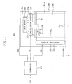
- FIG. 1 is a block diagram illustrating a liquid crystal display apparatus according to an exemplary embodiment of the present invention.
- a liquid crystal display apparatus 600 includes a gate driver 200, a data driver 300 and a liquid crystal display panel 100 that displays an image.
- a line selection circuit 400 drives the liquid crystal display panel 100.
- a controller 500 outputs a horizontal control signal HCS for controlling the gate driver 200, a vertical control signal VCS for controlling the data driver 300 and a selection control signal TG for controlling the line selection circuit 400.
- the liquid crystal display panel 100 includes a first substrate, a second substrate facing the first substrate and a liquid crystal layer interposed between the first and second substrates.
- a region of the liquid crystal display panel 100 includes a display region DA for displaying an image, first and second peripheral regions SA1 and SA2 disposed adjacent to the display region DA.
- the display region DA includes a gate line group having first to n-th gate lines GL1 to GLn, and a data line group having first to 2m-th data lines DL1 to DLm, wherein 'm' and 'n' are natural numbers greater than one.
- the gate lines GL1 to GLn are extended in a first direction D1
- the data lines DL1 to DL2m are extended in a second direction D2 that is substantially perpendicular to the first direction D1.
- a thin film transistor (TFT) 110 and a pixel electrode 120 are formed in 2m x n regions defined by the gate lines GL1 to GLn and the data lines DL1 to DL2m.
- the TFT 110 includes a gate electrode that is electrically connected to one of the gate lines GL1, a source electrode that is electrically connected to one of the data lines DL1, and a drain electrode that is electrically connected to the pixel electrode 120.
- the first peripheral region SA1 is adjacent to one end of the gate lines GL1 to GLn.
- the gate driver 200 is formed in the first peripheral region SA1 through a process through which the TFT 110 is formed.
- the gate driver 200 applies scan signals to the first gate line GL1 to n-th gate line GLn in sequence.
- the second peripheral region SA2 is adjacent to one end of the data lines DL1 to DL2m.
- the data driver 300 and the line selection circuit 400 are formed in the second peripheral region SA2.
- the data driver 300 is formed in a chip that is mounted on the second peripheral region SA2.
- the line selection circuit 400 is formed through the process through which the TFT 110 is formed.
- FIG. 2 is a schematic diagram illustrating a line selection circuit in FIG. 1.
- the data lines DL1 to DL2m formed in the display region DA include, for example, a first line block LB1 having odd numbered data lines DL1, DL3, ... DL2m-1, and a second line block LB2 having even numbered data lines DL2, DL4, ... DL2m.
- the first and second line blocks LB1 and LB2 may include arbitrary m-number of data lines, respectively.
- the data driver 300 outputs data signal through m-number of channels CH1 to CHm by a unit of block.
- the line selection circuit 400 includes the first selection block SB1 that is electrically connected to the first line block LB1, and a second selection block SB1 that is electrically connected to the second line block LB2.
- the line selection circuit 400 applies the data signal outputted from the data driver 300 by a unit of block to the first and second line blocks LB1 and LB2 with a clock time difference.
- the first selection block SB1 is disposed between the channels CH1 to CHm and the first line block LB1.
- the first selection block SB1 applies the data signal to the first line block LB1 in response to the first selection signal TG1 outputted from the data driver 300.
- the second selection block SB2 is disposed between the channels CH1 to CHm and the second line block LB2.
- the second selection block SB2 applies the data signal to the second line block LB2 in response to the second selection signal TG2 outputted from the data driver 300.
- the first and second selection signals TG1 and TG2 have opposite phase to each other. Therefore, the first and second selection blocks SB1 and SB2 are alternately turned on. That is, the line selection circuit 400 applies the data signal to the first and second line blocks LB1 and LB2 alternately.
- the first and second selection blocks SB1 and SB2 include a plurality of first and second selection switching devices SW1 and SW2, respectively.
- a transistor for example, may be employed as the first and second switching devices SW1 and SW2.
- the first switching device SW1 receives the first selection signal TG1 from the data driver 300 through a gate electrode, receives the data signal from the data driver through a source electrode, and applies the data signal to the odd numbered data lines DL1, DL3, ..., DL2m-1 of the first line block LB1 through a drain electrode.
- the second switching device SW2 receives the second selection signal TG2 from the data driver 300 through a gate electrode, receives the data signal from the data driver through a source electrode, and applies the data signal to the even numbered data lines DL2, DL4, ..., DL2m of the second line block LB2 through a drain electrode.
- the data lines DL1 to DL2m have, for example, a number that is two times greater than a number of the channels CH1 to CHm. Alternatively, the data lines may have three times or four times greater than the number of the channels CH1 to CHm. Then, the line selection circuit 300 applies the data signal to data line groups formed by dividing the data lines into three or four groups, and applies the data signal to the data line groups.
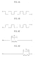
- FIGS. 3A and 3B are graphs illustrating waveforms of first and second selecting signals outputted from a gate driver in FIG. 1, respectively.
- FIGS. 3C and 3D are graphs illustrating waveforms of output patterns of first and third gate lines in n-number of gate lines, respectively.
- FIGS. 4A and 4B are graphs illustrating first and second selection signals outputted from a gate driver in FIG. 1, respectively.
- FIGS. 4C and 4D are graphs illustrating waveforms of output patterns of second and fourth gate lines in n-number of gate lines, respectively.
- a first active period T1 during which the scan signal is applied to the first gate line GL1 includes a first selection period t1 during which the first selection signal TG1 is high, and a second selection period t2 during which the second selection signal TG2 is high.
- the first and second selection periods t1 and t2 have a half-length of the first active period T1.
- a third active period T3 during which the scan signal is applied to the third gate line, GL3 includes a fifth selection period t5 during which the first selection signal TG1 is high, and a sixth selection period t6 during which the second selection signal TG2 is high.
- the fifth and sixth selection periods t5 and t6 have a half-length of the third active period T3.
- a second active period T2 during which the scan signal is applied to the second gate line GL2 includes a third selection period t3 during which the second selection signal TG2 is high, and a fourth selection period t4 during which the first selection signal TG1 is high.
- the third and fourth selection periods t3 and t4 have a half-length of the first active period T2.
- a fourth active period T4 during which the scan signal is applied to the fourth gate line GL4 includes a seventh selection period t7 during which the second selection signal TG2 is high, and a eighth selection period t8 during which the first selection signal TG1 is high.
- the seventh and eighth selection periods t7 and t8 have a half-length of the fourth active period T4.
- the first selection block SB1 is firstly turned on in response to the first selection signal TG1, and then the second selection block SB2 is turned on in response to the second selection signal TG2.
- the second selection block SB2 is firstly turned on in response to the second selection signal TG2, and then the first selection block SB1 is turned on in response to the first selection signal TG1.
- the second selection block SB2 is firstly turned on in response to the second selection signal TG2, and then the first selection block SB1 is turned on in response to the first selection signal TG1.
- the first selection block SB1 is firstly turned on in response to the first selection signal TG1, and then the second selection block SB2 is turned on in response to the second selection signal TG2.
- the data signal may be applied to the first and second line blocks LB1 and LB2 with a clock time difference at the first to fourth active periods T1 to T4.
- a sequence for selecting the first and second line blocks LB1 and LB2 may be changed according to the gate line.
- FIGS. 5A to 5D are graphs illustrating output signal of a line selection circuit in odd-numbered frames
- FIG. 6 is a schematic view illustrating a polarity of a data signal of each pixel region.
- 'one frame' is referred to a time from a first time point at which a scan signal is applied to the first gate line to a last time point at which the scan signal is applied to the last gate line. That is, 'one frame' is a time for activating the first gate line to the last gate line. For example, when the frame changed 64 times per a second, 'odd frames' referred to odd numbered frames of 64 frames.
- first to fourth gate lines GL1 to GL4 on n-th gate lines and only first to tenth data lines DL1 to DL10 of 2m-th data lines are shown.
- a solid line represents a first data signal applied to the data lines of the first block
- a dotted line represents a second data signal applied to the data lines of the second block.
- a hatched region corresponds to bright pixel regions 603 and 605, and non-hatched region corresponds to a dark pixel region 601.
- the scan signal is applied to the first gate line GL1 during the first active period T1 in FIG. 3.
- the first data signal is applied to the first line block LB1 in FIG. 2 during the first selection period t1 of the first active period T1
- the second data signal is applied to the second line block LB2 during the second selection period t2 of the first active period T1.
- the first data signal is applied to the first line block LB1 in response to the first selection signal TG1 that is high in the first selection period t1.
- the second data signal is applied to the second line block LB2 in response to the second selection signal TG2 that is high in the second selection period t2.
- the data signal is firstly applied to the odd numbered gate lines, and then the data signal is applied to the even numbered gate lines.
- the data signal is applied firstly to the even number gate lines, and then the data signal is applied to the odd numbered gate lines.
- a positive polarity of the first and second data signals has a higher voltage than a common voltage Vcom
- a negative polarity of the first and second data signals has a lower voltage than the common voltage Vcom
- the first data signal of positive polarity is applied to the first, fifth and ninth data lines DL1, DL5 and DL9 and the first data signal of negative polarity is applied to the third and seventh data lines DL3 and DL7 during the first selection period t1.
- the second data signal of positive polarity is applied to the second, sixth and tenth data lines DL2, DL6 and DL10 and the second data signal of negative polarity is applied to the fourth and eighth data lines DL4 and DL8 during the second selection period T2.
- the first data signal applied to the first line block LB1 and the second data signal applied to the second line block LB2 have same polarity.
- the scan signal is applied to the second gate line GL2 during the second active period T2 and the second data signal is applied to the second line block LB2 during the third selection period t3 of the second active period T2.
- the first data signal is applied to the first line block LB1.
- the second data signal of negative polarity is applied to the second, sixth and tenth data lines DL2, DL6 and DL10 and the second data signal of positive polarity is applied to the fourth and eighth data lines DL4 and DL8.
- the first data signal of positive polarity is applied to the first, fifth and ninth data lines DL1, DL5 and DL9 and the first data signal of negative polarity is applied to the third and seventh data lines DL3 and DL7.
- a polarity of the first and second data signals is same as a polarity of a signal of the first and second data signals outputted in the first active period T1 and shifted in a third direction D3 in FIG. 6 by one pixel region. That is, the second data signal applied to the second line block LB2 during the first active period T1 is applied to the first line block LB1 as the first data signal during the second active period T2. Therefore, the first data signal applied to the first line block LB1 during the second active period T2 has a different polarity from a polarity of the second data signal applied to the second line block LB2.
- the scan signal is applied to the third gate line GL3 during the third active period T3 and the first data signal is applied to the first line block LB1 during the fifth selection period t5 of the third active period T3.
- the second data signal is applied to the second line block LB2 during the sixth selection period.
- the first data signal of negative polarity is applied to the first, fifth and ninth data lines DL1, DL5 and DL9
- the first data signal of positive polarity is applied to the third and seventh data lines DL3 and DL7 during the fifth selection period t5.
- the second data signal of negative polarity is applied to the second, sixth and tenth data lines DL2, DL6 and DL10, and the second data signal of positive polarity is applied to the fourth and eighth data lines DL4 and DL8 during the sixth selection period t6.
- a polarity of the first and second data signals is same as a polarity of a signal of the first and second data signals outputted in the second active period T2 and shifted in the third direction D3 in FIG. 6 by one pixel region. Therefore, the first data signal applied to the first line block LB1 during the third active period T3 has a same polarity as a polarity of the second data signal applied to the second line block LB2.
- the scan signal is applied to the fourth gate line GL4, and the second data signal is applied to the second line block LB2 during the seventh selection period t7 of the fourth active period T4.
- the first data signal is applied to the first line block LB1 during the eighth selection period t8 of the fourth active period T4.
- the second data signal of positive polarity is applied to the second, sixth and tenth data lines DL2, DL6 and DL10, and the second data signal of negative polarity is applied to the fourth and eighth data lines DL4 and DL8 during the seventh selection period t7.
- the first data signal of negative polarity is applied to the first, fifth and ninth data lines DL1, DL5 and DL9, and the first data signal of positive polarity is applied to the third and seventh data lines DL3 and DL7 during the eighth selection period t8.
- a polarity of the first and second data signals is same as a polarity of a signal of the first and second data signals outputted in the third active period T3 and shifted in the third direction D3 in FIG. 6 by one pixel region. Therefore, the first data signal applied to the first line block LB1 during the fourth active period T4 has a different polarity from a polarity of the second data signal applied to the second line block LB2.
- the bright pixel regions 603 and 605 and the dark pixel region 601 are formed alternately on a screen of the liquid crystal display apparatus. Therefore, the bright pixel regions 603 and 605 offset the dark region 601 to uniformize luminance of the liquid crystal display apparatus.
- FIGS. 7A to 7D are graphs illustrating output signal of a line selection circuit in even-numbered frames
- FIG. 8 is a schematic view illustrating a polarity of a data signal of each pixel region. 'Even frames' represent even numbered frames of 64 frames.
- a solid line represents a first data signal applied to the data lines of the first block
- a dotted line represents a second data signal applied to the data lines of the second block.
- a hatched region corresponds to bright pixel regions 803 and 805, and non-hatched region corresponds to a dark pixel region 801.
- the first data signal of a negative polarity is applied to the first, fifth and ninth data lines DL1, DL5 and DL9, and the first data signal of a positive polarity is applied to the third and seventh data lines DL3 and DL7 during the first selection period t1 of the first active period T1 during which the scan signal is applied to the first gate line GL1.
- the second data signal of a negative polarity is applied to the second, sixth and tenth data lines DL2, DL6 and DL10 and the second data signal of a positive polarity is applied to the fourth and eighth data lines DL4 and DL8 during the second selection period t2.
- the first data signal of a positive polarity is applied to the second, sixth and tenth data lines DL2, DL6 and DL10, and the first data signal of a negative polarity is applied to the fourth and eighth data lines DL4 and DL8 during the third selection period of the second active period T2 during which the scan signal is applied to the second gate line GL2.
- the second data signal of a negative polarity is applied to the first, fifth and ninth data lines DL1, DL5 and DL9 and the second data signal of a positive polarity is applied to the third and seventh data lines DL3 and DL7.
- the first data signal of a positive polarity is applied to the first, fifth and ninth data lines DL1, DL5 and DL9 and the first data signal of a negative polarity is applied to the third and seventh data lines DL3 and DL7 during the fifth selection period t5 of the third active period T3 during which the scan signal is applied to the third gate line GL3.
- the second data signal of a positive polarity is applied to the second, sixth and tenth data lines DL2, DL6 and DL10
- the second data signal of a negative polarity is applied to the fourth and eighth data lines DL4 and DL8 during the sixth selection period.
- the second data signal of a negative polarity is applied to the second, sixth and tenth data lines DL2, DL6 and DL10, and the second data lines of a positive polarity is applied to the fourth and eighth data lines DL2 and DL8 during the seventh selection period t7 of the fourth active period T4 during which the scan signal is applied to the fourth gate line GL4.
- the first data signal of a positive polarity is applied to the first, fifth and ninth data lines DL1, DL5 and DL9
- the first data signal of a negative polarity is applied to the third and seventh data lines DL3 and DL7 during the eighth selection period t8.
- the bright pixel regions 803 and 805 and the dark pixel region 801 are formed alternately on a screen of the liquid crystal display apparatus. Therefore, the bright pixel regions 803 and 805 offset the dark region 801 to uniformize luminance of the liquid crystal display apparatus.
- a polarity of the data signal applied to the pixel at odd frames is different from a polarity of the data signal applied to the pixel at even frames.
- the bright pixel regions 603 and 605 of the odd frames correspond to the bright pixel regions 803 and 805 of the even frames. Therefore, the liquid crystal displays apparatus displays an image of which luminance is uniform even when the frame is changed.
- a number of the data lines formed on the liquid crystal display panel is two times greater than a number of output terminals of the data driver. Therefore, the data lines are divided into two blocks. Alternatively, as a resolution increases, the number of the data lines may be three, four or more times greater than the number of the output terminals of the data driver.
- m-number of data signals are divided into m/i number of data signals.
- a polarity of each m/i number of data signals is shifted and the data driver outputs the m/i number of data signals i-times.
- the line selection circuit applies the m/i number of data signals to each block and varies a time for selecting the block.
- the bright pixel region and the dark pixel region are alternately formed to offset the difference. Therefore, a luminance of the liquid crystal display apparatus is uniformized to enhance a display quality.
Landscapes
- Physics & Mathematics (AREA)
- Engineering & Computer Science (AREA)
- General Physics & Mathematics (AREA)
- Crystallography & Structural Chemistry (AREA)
- Chemical & Material Sciences (AREA)
- Theoretical Computer Science (AREA)
- Computer Hardware Design (AREA)
- Nonlinear Science (AREA)
- Mathematical Physics (AREA)
- Optics & Photonics (AREA)
- Control Of Indicators Other Than Cathode Ray Tubes (AREA)
- Liquid Crystal (AREA)
- Liquid Crystal Display Device Control (AREA)
Applications Claiming Priority (2)
| Application Number | Priority Date | Filing Date | Title |
|---|---|---|---|
| KR2003071041 | 2003-10-13 | ||
| KR1020030071041A KR20050035385A (ko) | 2003-10-13 | 2003-10-13 | 표시장치 및 이의 구동방법 |
Publications (2)
| Publication Number | Publication Date |
|---|---|
| EP1524647A2 true EP1524647A2 (de) | 2005-04-20 |
| EP1524647A3 EP1524647A3 (de) | 2007-07-18 |
Family
ID=34374262
Family Applications (1)
| Application Number | Title | Priority Date | Filing Date |
|---|---|---|---|
| EP04256258A Withdrawn EP1524647A3 (de) | 2003-10-13 | 2004-10-08 | Polaritätsumkehrungsverfahren für eine Anzeigevorrichtung mit aktiver Matrix |
Country Status (5)
| Country | Link |
|---|---|
| US (1) | US20050078075A1 (de) |
| EP (1) | EP1524647A3 (de) |
| JP (1) | JP2005122172A (de) |
| KR (1) | KR20050035385A (de) |
| TW (1) | TW200532633A (de) |
Families Citing this family (8)
| Publication number | Priority date | Publication date | Assignee | Title |
|---|---|---|---|---|
| KR101253273B1 (ko) * | 2005-12-16 | 2013-04-10 | 삼성디스플레이 주식회사 | 표시 장치 및 그 구동 방법 |
| KR20070115371A (ko) * | 2006-06-02 | 2007-12-06 | 삼성전자주식회사 | 표시 장치와, 이의 구동 장치 및 방법 |
| US20080150862A1 (en) * | 2006-12-26 | 2008-06-26 | Sheng-Pin Tseng | Lcd device capable of reducing line flicker and horizontal crosstalk for rgbw subpixel arrangement |
| TW200933583A (en) * | 2008-01-30 | 2009-08-01 | Chunghwa Picture Tubes Ltd | Source driving circuit |
| TWI393107B (zh) * | 2008-07-02 | 2013-04-11 | Au Optronics Corp | 液晶顯示裝置 |
| US11017709B2 (en) * | 2018-03-02 | 2021-05-25 | Xianyang Caihong Optoelectronics Technology Co., Ltd | Driving method for pixel matrix and display device |
| CN109032409B (zh) * | 2018-07-26 | 2021-11-02 | 京东方科技集团股份有限公司 | 一种显示面板的驱动方法、显示面板及显示装置 |
| CN110648639B (zh) * | 2019-09-27 | 2022-07-08 | 京东方科技集团股份有限公司 | 一种液晶显示器及其驱动方法、装置 |
Family Cites Families (2)
| Publication number | Priority date | Publication date | Assignee | Title |
|---|---|---|---|---|
| JP4031291B2 (ja) * | 2001-11-14 | 2008-01-09 | 東芝松下ディスプレイテクノロジー株式会社 | 液晶表示装置 |
| JP3791452B2 (ja) * | 2002-05-02 | 2006-06-28 | ソニー株式会社 | 表示装置およびその駆動方法、ならびに携帯端末装置 |
-
2003
- 2003-10-13 KR KR1020030071041A patent/KR20050035385A/ko not_active Ceased
-
2004
- 2004-10-08 EP EP04256258A patent/EP1524647A3/de not_active Withdrawn
- 2004-10-12 US US10/961,190 patent/US20050078075A1/en not_active Abandoned
- 2004-10-13 TW TW093131032A patent/TW200532633A/zh unknown
- 2004-10-13 JP JP2004298524A patent/JP2005122172A/ja not_active Withdrawn
Also Published As
| Publication number | Publication date |
|---|---|
| TW200532633A (en) | 2005-10-01 |
| EP1524647A3 (de) | 2007-07-18 |
| US20050078075A1 (en) | 2005-04-14 |
| JP2005122172A (ja) | 2005-05-12 |
| KR20050035385A (ko) | 2005-04-18 |
Similar Documents
| Publication | Publication Date | Title |
|---|---|---|
| KR100945581B1 (ko) | 액정 표시 장치 및 그 구동 방법 | |
| CN100538449C (zh) | 液晶显示器 | |
| KR101171176B1 (ko) | 박막 트랜지스터 표시판 및 표시 장치 | |
| JP2937130B2 (ja) | アクティブマトリクス型液晶表示装置 | |
| CN100511384C (zh) | 液晶显示面板 | |
| KR101319345B1 (ko) | 액정 표시장치의 구동장치와 그 구동방법 | |
| KR20080076129A (ko) | 표시 장치의 구동 장치 및 이를 포함하는 표시 장치 | |
| TWI375211B (en) | Liquid crystal display device | |
| KR19990078078A (ko) | 액정표시장치 | |
| KR20070098591A (ko) | 표시장치 및 이의 구동방법 | |
| KR20030083309A (ko) | 액정표시장치 | |
| KR100322822B1 (ko) | 액정패널및액정표시장치 | |
| US7079164B2 (en) | Method and apparatus for driving liquid crystal display panel | |
| KR102169032B1 (ko) | 표시장치 | |
| KR20150005259A (ko) | 표시 패널 및 이를 포함하는 표시 장치 | |
| CN119296488A (zh) | 显示面板和驱动方法 | |
| KR20080109159A (ko) | 액정 표시장치 및 그의 구동방법 | |
| JPH11282434A (ja) | 平面表示装置 | |
| EP1524647A2 (de) | Polaritätsumkehrungsverfahren für eine Anzeigevorrichtung mit aktiver Matrix | |
| JP3957403B2 (ja) | 液晶表示装置およびその駆動方法 | |
| US20060279506A1 (en) | Apparatus and method of driving liquid crystal display apparatus | |
| KR20010017524A (ko) | 도트 반전 구동 방식의 박막 트랜지스터 액정 표시 장치 | |
| KR20090047691A (ko) | 액정 표시장치의 구동장치와 그 구동방법 | |
| KR101286514B1 (ko) | 액정표시장치 | |
| KR100446378B1 (ko) | 액정표시소자 및 그 구동방법 |
Legal Events
| Date | Code | Title | Description |
|---|---|---|---|
| PUAI | Public reference made under article 153(3) epc to a published international application that has entered the european phase |
Free format text: ORIGINAL CODE: 0009012 |
|
| 17P | Request for examination filed |
Effective date: 20041020 |
|
| AK | Designated contracting states |
Kind code of ref document: A2 Designated state(s): AT BE BG CH CY CZ DE DK EE ES FI FR GB GR HU IE IT LI LU MC NL PL PT RO SE SI SK TR |
|
| AX | Request for extension of the european patent |
Extension state: AL HR LT LV MK |
|
| PUAL | Search report despatched |
Free format text: ORIGINAL CODE: 0009013 |
|
| AK | Designated contracting states |
Kind code of ref document: A3 Designated state(s): AT BE BG CH CY CZ DE DK EE ES FI FR GB GR HU IE IT LI LU MC NL PL PT RO SE SI SK TR |
|
| AX | Request for extension of the european patent |
Extension state: AL HR LT LV MK |
|
| AKX | Designation fees paid |
Designated state(s): DE FR GB |
|
| 17Q | First examination report despatched |
Effective date: 20080401 |
|
| STAA | Information on the status of an ep patent application or granted ep patent |
Free format text: STATUS: THE APPLICATION IS DEEMED TO BE WITHDRAWN |
|
| 18D | Application deemed to be withdrawn |
Effective date: 20080812 |