EP1524698B1 - Procédé de fabrication d'un convertisseur photoélectrique - Google Patents
Procédé de fabrication d'un convertisseur photoélectrique Download PDFInfo
- Publication number
- EP1524698B1 EP1524698B1 EP05000489A EP05000489A EP1524698B1 EP 1524698 B1 EP1524698 B1 EP 1524698B1 EP 05000489 A EP05000489 A EP 05000489A EP 05000489 A EP05000489 A EP 05000489A EP 1524698 B1 EP1524698 B1 EP 1524698B1
- Authority
- EP
- European Patent Office
- Prior art keywords
- substrates
- layer
- photoelectric converter
- photoelectric conversion
- photoelectric
- Prior art date
- Legal status (The legal status is an assumption and is not a legal conclusion. Google has not performed a legal analysis and makes no representation as to the accuracy of the status listed.)
- Expired - Lifetime
Links
Images



Classifications
-
- H—ELECTRICITY
- H10—SEMICONDUCTOR DEVICES; ELECTRIC SOLID-STATE DEVICES NOT OTHERWISE PROVIDED FOR
- H10W—GENERIC PACKAGES, INTERCONNECTIONS, CONNECTORS OR OTHER CONSTRUCTIONAL DETAILS OF DEVICES COVERED BY CLASS H10
- H10W90/00—Package configurations
-
- H—ELECTRICITY
- H10—SEMICONDUCTOR DEVICES; ELECTRIC SOLID-STATE DEVICES NOT OTHERWISE PROVIDED FOR
- H10F—INORGANIC SEMICONDUCTOR DEVICES SENSITIVE TO INFRARED RADIATION, LIGHT, ELECTROMAGNETIC RADIATION OF SHORTER WAVELENGTH OR CORPUSCULAR RADIATION
- H10F39/00—Integrated devices, or assemblies of multiple devices, comprising at least one element covered by group H10F30/00, e.g. radiation detectors comprising photodiode arrays
- H10F39/10—Integrated devices
- H10F39/107—Integrated devices having multiple elements covered by H10F30/00 in a repetitive configuration, e.g. radiation detectors comprising photodiode arrays
-
- H—ELECTRICITY
- H10—SEMICONDUCTOR DEVICES; ELECTRIC SOLID-STATE DEVICES NOT OTHERWISE PROVIDED FOR
- H10F—INORGANIC SEMICONDUCTOR DEVICES SENSITIVE TO INFRARED RADIATION, LIGHT, ELECTROMAGNETIC RADIATION OF SHORTER WAVELENGTH OR CORPUSCULAR RADIATION
- H10F39/00—Integrated devices, or assemblies of multiple devices, comprising at least one element covered by group H10F30/00, e.g. radiation detectors comprising photodiode arrays
- H10F39/10—Integrated devices
- H10F39/12—Image sensors
- H10F39/18—Complementary metal-oxide-semiconductor [CMOS] image sensors; Photodiode array image sensors
-
- H—ELECTRICITY
- H10—SEMICONDUCTOR DEVICES; ELECTRIC SOLID-STATE DEVICES NOT OTHERWISE PROVIDED FOR
- H10F—INORGANIC SEMICONDUCTOR DEVICES SENSITIVE TO INFRARED RADIATION, LIGHT, ELECTROMAGNETIC RADIATION OF SHORTER WAVELENGTH OR CORPUSCULAR RADIATION
- H10F39/00—Integrated devices, or assemblies of multiple devices, comprising at least one element covered by group H10F30/00, e.g. radiation detectors comprising photodiode arrays
- H10F39/10—Integrated devices
- H10F39/12—Image sensors
- H10F39/18—Complementary metal-oxide-semiconductor [CMOS] image sensors; Photodiode array image sensors
- H10F39/189—X-ray, gamma-ray or corpuscular radiation imagers
- H10F39/1898—Indirect radiation image sensors, e.g. using luminescent members
-
- H—ELECTRICITY
- H10—SEMICONDUCTOR DEVICES; ELECTRIC SOLID-STATE DEVICES NOT OTHERWISE PROVIDED FOR
- H10F—INORGANIC SEMICONDUCTOR DEVICES SENSITIVE TO INFRARED RADIATION, LIGHT, ELECTROMAGNETIC RADIATION OF SHORTER WAVELENGTH OR CORPUSCULAR RADIATION
- H10F39/00—Integrated devices, or assemblies of multiple devices, comprising at least one element covered by group H10F30/00, e.g. radiation detectors comprising photodiode arrays
- H10F39/10—Integrated devices
- H10F39/12—Image sensors
- H10F39/191—Photoconductor image sensors
- H10F39/195—X-ray, gamma-ray or corpuscular radiation imagers
-
- H—ELECTRICITY
- H10—SEMICONDUCTOR DEVICES; ELECTRIC SOLID-STATE DEVICES NOT OTHERWISE PROVIDED FOR
- H10F—INORGANIC SEMICONDUCTOR DEVICES SENSITIVE TO INFRARED RADIATION, LIGHT, ELECTROMAGNETIC RADIATION OF SHORTER WAVELENGTH OR CORPUSCULAR RADIATION
- H10F39/00—Integrated devices, or assemblies of multiple devices, comprising at least one element covered by group H10F30/00, e.g. radiation detectors comprising photodiode arrays
- H10F39/80—Constructional details of image sensors
- H10F39/803—Pixels having integrated switching, control, storage or amplification elements
-
- H—ELECTRICITY
- H10—SEMICONDUCTOR DEVICES; ELECTRIC SOLID-STATE DEVICES NOT OTHERWISE PROVIDED FOR
- H10F—INORGANIC SEMICONDUCTOR DEVICES SENSITIVE TO INFRARED RADIATION, LIGHT, ELECTROMAGNETIC RADIATION OF SHORTER WAVELENGTH OR CORPUSCULAR RADIATION
- H10F39/00—Integrated devices, or assemblies of multiple devices, comprising at least one element covered by group H10F30/00, e.g. radiation detectors comprising photodiode arrays
- H10F39/80—Constructional details of image sensors
- H10F39/809—Constructional details of image sensors of hybrid image sensors
Definitions
- the present invention relates to a manufacturing method of a photoelectric converter, and in particular, to a manufacturing method of a two-dimensional photoelectric converter that is used for facsimile machines, digital copy machines, and X-ray machines.
- a scanning system that employs a reducing optical system and a CCD sensor is used for a scanning apparatus, such as a facsimile machine or a digital copy machine.
- a scanning apparatus such as a facsimile machine or a digital copy machine.
- photoelectric conversion semiconductor material such as amorphous silicon (hereinafter referred to as a-Si)
- a so-called close-contact sensor has been developed for which a photoelectric conversion device and a signal processor are formed on a large substrate, and by which data are scanned by using an optical system that has the same magnification rate as that of a data source.
- a-Si can be employed not only as a photoelectric conversion material but also as a thin film field-effect transistor film (hereinafter referred to as a TFT), both a photoelectric conversion semiconductor layer and a TFT semiconductor layer can be formed at the same time.
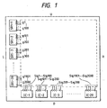
- Figs. 1 and 2 are plan views of a photoelectric converter that has 2000 x 2000 pixels.
- the number of photoelectric conversion devices that are included in an arrangement are increased in both the vertical and the horizontal directions.
- 2000 control lines scan lines
- 2000 signal lines data lines
- the sizes of a scanning circuit and an integrated circuit used for detection are increased because they have to control and handle 2000 signal lines.
- Fig. 1 20 chips (SR1-1 through SR1-20) are mounted along the left side (L) and another 20 chips (IC-1 through IC-20) are mounted across the down side (D). Connected to each chip by wire bonding are 100 control lines or signal lines.
- the portion that is enclosed by broken lines in Fig. 1 corresponds to a photoelectric conversion device array that is arranged as a two-dimensional area. The connection of the detection integrated circuit to an external device is not shown.
- 10 chips are mounted along the left side (L) and 10 chips (SR1-11 through SR1-20) are mounted along the right side (R); and 10 chips (IC-1 through IC-10) are mounted across the upper side (U) and 10 chips (IC-11 through IC-20) are mounted across the down side (D). Since in this structure 1000 lines are provided at each of the upper, down, left and right sides (U, D, L and R), the density of the lines arranged along each side is reduced and the concentration of the wire bonding required on each side is also decreased, thus providing an increased manufacturing yielding ratio.
- Lines g1, g3, g5, ..., and g1999 are arranged along the left side (L), while g2, g4, g6, ..., and g2000 are arranged along the right side (R). That is, the odd numbered control lines are distributed along the left side (L), and the even numbered control lines are distributed along the right side (R). With this arrangement, since each line is pulled out so that the liens are located at equal intervals, the lines are not overly concentrated and the yielding ratio is increased.
- the wiring across the upper side (U) and the down side (D) is performed in the same manner.
- lines g1 through g201 through g300, ..., and g1801 through g1900 are provided on the left side (L), while lines g101 through g200, g301 through g400, ..., and g1901 through g2000 are provided on the right side (R).
- L left side
- R right side
- contiguous control lines it is possible for contiguous control lines to be distributed to each chip and for these chips to be alternately sorted to the left side and to be right side (to L and to R).
- the control lines for a single chip can be controlled sequentially, the adjustment and the setup of drive timing can be facilitated, a circuit does not become complicated, and an inexpensive IC can be used.
- the same arrangement can be applied for upper side and the down side (U and D), and an inexpensive IC that can perform a continuous process can be used.
- the size of the resultant device having large dimensions is limited to a multiple of the original substrate size, such as twice, four times, or six times the size.
- connection lines lines for connecting control lines to the output terminals of the scan circuits
- the structure of the connection lines becomes complicated and expensive, and the high-density mounting of scan circuits is prevented.
- Two types of ICs are prepared for which the orders in which output terminals are located differ, and ICs of one type are arranged on the left, while ICs of the other type are arranged on the right.
- the manufacture of two types of ICs even though their basic operations are the same, results in higher manufacturing costs.
- Document EP-A-0 660 421 discloses a photoelectric converter of a high signal-to-noise ratio, low cost, high productivity and stable characteristics and a system including the above photoelectric converter.
- the photoelectric converter includes a photoelectric converting portion in which a first electrode layer, an insulating layer for inhibiting carriers from transferring, a photoelectric converting semiconductor layer of a non-single-crystal type, an injection blocking layer for inhibiting a first type of carriers from being injected into the semiconductor layer and a second electrode layer are laminated in this order on an insulating substrate.
- Document EP-A-0 555 907 discloses a large area active matrix array, that is manufactured by providing four substrates carrying a sub-array having an active area comprising a matrix of switching elements and associated row and column conductors for enabling addressing of individual switching elements.
- a first object of the present invention to reduce a manufacturing costs for a photoelectric converter having large dimensions by providing an increased yielding ratio for each substrate during fabrication of photoelectric converter having large dimensions, and by reducing losses due to defects in each substrate.
- the cost of manufacturing a photoelectric converter having large dimensions can be reduced.
- the connections for driving circuits need not be increased and need not be complicated.
- the resultant device size can be varied.
- a photoelectric converter wherein the amount of incident light can be detected as the photoelectric conversion device has only one introduction prevention layer, can be provided at a low price; the optimizing of the process is easy and the yielding ratio can be increased; the manufacturing cost can be reduced; and the SN ratio is high.
- the exposure apparatus that employs the above converter differs from conventional X-ray film in that it can project its output very quickly, and in that image processing and data storage are also possible. It has better sensitivity than the film, and a clear image can be obtained with a weak X-ray that will have little adverse effect on a human body.
- the characteristics of the photoelectric conversion devices on different substrates that are at the least located at positions adjacent to each other on different substrates can be sequentially equalized.
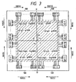
- Fig. 3 is a plan view of the overall structure of a photoelectric converter according to a first embodiment of the present invention.
- the reference numerals are used to denote corresponding or identical components in Figs. 1 and 2 , and no explanation will be given for them.
- photoelectric converters 100, 200, 300 and 400 mounted on four substrates are bonded with no gaps between them, to constitute a single large photoelectric converter.
- each substrate 100 Located on each substrate 100, on which the photoelectric conversion device array is to be mounted, are 1000 x 1000 photoelectric devices (shaded portion) that are connected to 2000 lines, i.e., 1000 control lines g1 through g1000 and 1000 signal lines sig1 through sig1000. And as there are 100 scan circuits SR1 formed on a single IC chip, there are a total of 10 IC chips SR1 through SR1-10 located on the substrate 100, the IC chips being connected to the respective control lines g1 through g1000.
- 100 processing circuits are integrated on a single IC chip, with 10 detection integrated circuit chips, IC-1 through IC-10, being located on each substrate and with the IC chips being connected to the signal lines sig1 through sig1000.
- the other substrates 200, 300 and 400, on which the photoelectric conversion device arrays are mounted have the same structured as the substrate 100, and have 1000 x 1000 photoelectric conversion devices arranged on it that are connected to 1000 control lines and 1000 signal lines. Also provided are 10 of the scan circuits and 10 of the detection integrated circuits. Although for each substrate these scan circuits and the integrated circuits may differ, it is preferable that a single type of IC be used for all the substrates, as will be described later. Thus, the four photoelectric conversion device arrays on the four substrates can be scanned at the same time. In this case, when compared with the example shown in Fig. 1 , the period of time required for the scanning can be reduced to 1/4 of that required for the example in Fig. 1 .
- the scan circuits SR1-1 through SR1-10 employ the direction indicated by arrow 100ss, while the detection circuits IC-1 through IC-10 employ the direction indicated by arrow 100SI.
- the device shown in Fig. 3 is so structured that the substrates on which are mounted the photoelectric conversion arrays having the same structure are rotated 90° relative to each other and positioned.
- the upper left substrate 100 is rotated clockwise 90° around point pp, it is located at the position for the upper right substrate 100.
- the substrate 100 is rotated a further 90°, it reaches the position for the lower right substrate 100.
- the substrate 100 is rotated another 90°, it reaches the position for the lower left substrate 100.
- the position of the lower left substrate 100 is where the upper left substrate 100 is located when from its upper left position it is rotated 90° counterclockwise around point pp.
- the scan circuits SR1-1 through SR1-10 and the detection circuits IC-1 through IC-10 are respectively arranged along the four sides of the photoelectric converter having large dimensions.
- the scan direction 100SS for the scan circuits on the individual sides is the opposite of the scan direction 100SI for the detection circuits.
- either one of the scan directions can be reversed, so that the scan directions for the scan circuits and the detection circuits along each of the sides are the same.
- Signals that are output by the detection circuits IC-1 through IC-10 on the four substrates are stored in four memories (not shown), which are provided for corresponding substrates. Coordinate transformation is performed on the signals as needed so that they correspond to physical pixel coordinates in Fig. 3 . As a result, the image of an input object can be reproduced on a display device.
- the scan circuit has a shift register that shifts in a single direction, and the scan direction is determined by the shift direction of the shift register.
- the detection circuit also has a shift register that shifts in a single direction, and the order in which signals are fetched or the order in which the fetched signals are output (the scan direction) is determined by the shift direction of the shift register.
- the driving circuit for the photoelectric converter can be formed.
- the cost of manufacturing the driving circuit is not high.
- the photoelectric device arrays are fabricated on the four substrates, as is shown in Fig. 3 , and the four substrates are bonded together with as a small gap as possible between them, so that a photoelectric converter having large dimensions can be constituted.
- the yielding ratio for each substrate can be increased, and the losses that are incurred due to defects on the individual substrates can be reduced.
- the total length of all of the control lines and all of the signal lines for the substrates in Fig. 3 is about 1/4 the total length of all the control lines and signal lines for the photoelectric converter in Fig. 1 .
- a short circuit or an open circuit in a control line or in a signal line causes all of the output signals of the photoelectric conversion devices connected to the line to become inaccurate, and the photoelectric converter can not be employed.
- the possibility of the occurrence of such a defect is substantially proportional to the total length of all the control lines and signal lines, and as a result of such a defect, the yielding ratio will be reduced.
- a yielding ratio due to a defect in the wiring for each substrate in Fig. 3 is about four times the yielding ratio for the photoelectric converter shown in Fig. 1 .
- the loss that is occasioned when a defect occurs on one substrate shown in Fig. 3 and the photoelectric converter can not be used is proportionate to the dimensions of all the substrates. The loss, therefore, is about 1/4 of that experienced as a loss by the photoelectric converter in Fig. 1 when a defect occurs and the converter can not be used.
- photoelectric conversion devices each of which is a laminate composed of a first electrode layer 2, an insulating layer 7, a semiconductor layer 4 that can perform photoelectric conversion, a semiconductor layer 5 for preventing introduction of a first conductive carrier, and a second electrode layer 6.
- the photoelectric converter comprises: photoelectric conversion means for accumulating, on the semiconductor layer 5, the first conductive carrier, which is induced by signal light that enters the semiconductor layer 5, and for providing an electric field to a light receiving device in a direction in which the second conductive carrier, which differs from the first conductive carrier, is to be guided to the second electrode layer 6; refresh means for providing an electric field for the light receiving devices in a direction in which the first conductive carrier is to be guided from the semiconductor layer to the second electrode layer; and a signal detector for detecting the first conductive carrier, which is accumulated on the semiconductor layer, or the second conductive carrier, which is guided to the second electrode layer, during photoelectric conversion performed by the photoelectric conversion means.
- S11 denotes a light-receiving device; T11, a TFT; C11, a capacitor, and SIG, a signal line.
- the capacitor C12 and the light-receiving device S11 are not separated from each other, and they can be integrally formed because the light-receiving device, the capacitor and the TFT have substantially the same layer structure.
- a silicon nitride film SiN is deposited as a passivated film on the upper portion of a pixel. When light enters the photoelectric conversion device from upward, the light is converted into an electric signal (accumulated electric change amount).
- a photoelectric converter according to a second embodiment of the present invention is the same as that shown in Fig. 3 .
- photoelectric conversion device arrays on four substrates have the same structure. Further, the four substrates on which the photoelectric conversion devices are mounted are rotated 90° each other in a plane and are bonded together with no gaps to provide a single large photoelectric converter. The arrays having the same structure are fabricated through the same manufacturing process.
- each substrate 100 Located on each substrate 100 are 1000 x 1000 photoelectric devices that are connected to 2000 lines, i.e., 1000 control lines g1 through g1000 and 1000 signal lines sig1 through sig1000. And as there are 100 scan circuits SR1 integrated on a single IC chip, there are a total of 10 IC chips SR1 through SR1-10 located on the substrate 100, the IC chips being connected to the respective control lines g1 through g1000.
- the detection integrated circuits 100 processing circuits are integrated on a single IC chip, with 10 detection integrated circuit chips, IC-1 through IC-10, being located on each substrate and with the IC chips being connected to the signal lines sig1 through sig1000.
- the same scan circuits and the integrated circuits are used for all the substrates.
- the four photoelectric conversion device arrays on the four substrates can be scanned at the same time. In this case, when compared with the example shown in Fig. 9 , the period of time required for the scanning can be reduced to 1/4 of that required for the example in Fig. 9 .
- the four substrates are prepared on which photoelectric conversion devices and wiring at a predetermined pattern are formed. On each of the substrates, the scan circuits and detection integrated circuits are mounted. The resultant four substrates are rotated 90° and are bonded together with no gaps between them, so as to constitute a photoelectric converter having large dimensions. As a result, the number of required components can be reduced.
- the inspection procedure can be performed by two types of devices, and the efficiency of the inspection procedure and the accompanying throughput can be increased. As a result, the cost of manufacturing a photoelectric converter having large dimensions can be reduced.
- Fig. 6 is a plan view of a photoelectric converter according to a third embodiment of the present invention.
- the same reference numerals as are used in Figs. 1 through 3 are used to denote corresponding or identical components.
- the feature of the photoelectric converter in Fig. 6 is that the number of photoelectric conversion devices in photoelectric conversion device arrays, or the shapes in a plane of the arrays, one of which is mounted on each of four substrates, differ.
- the difference between the upper right substrate in Fig. 3 and an upper right substrate 220 in Fig. 6 is that the number of photoelectric conversion devices has been reduced from 1000 ⁇ 1000 to 700 ⁇ 1000. Accordingly, the number of signal lines is reduced from 1000 to 700, and the number of integrated detection circuits is reduced from ten to seven.
- the difference between the lower left substrate in Fig. 3 and a lower left substrate 440 in Fig. 6 is that the number of photoelectric conversion devices has been reduced from 1000 x 1000 to 1000 x 700. Accordingly, the number of signal lines is reduced from 1000 to 700, and the number of scan circuits is reduced from ten to seven.
- the difference between the lower right substrate in Fig. 3 and a lower right substrate 330 in Fig. 6 is that the number of photoelectric conversion devices has been reduced from 1000 x 1000 to 700 x 700. Accordingly, the number of the signal lines is reduced from 1000 to 700, and the number of scan circuits is reduced from ten to seven.
- the dimensions or the shape of the photoelectric conversion device portion of the photoelectric converter, which is constituted by bonding the four substrates together, can be changed.
- the photoelectric converter when the photoelectric converter is to be constituted by bonding four substrates together, normally, four substrates, on each of which is mounted a standard photoelectric conversion device array, are fabricated and bonded together.
- a small or a large resultant photoelectric conversion device array is desired, or when a resultant photoelectric conversion array having a different shape is desired, one, two or three substrates out of four are newly fabricated, and the substrate on which is mounted the standard photoelectric conversion device array is replaced by them. In this manner, a photoelectric converter for which four desired substrates are bonded together can be provided.
- the photoelectric converter shown in Fig. 3 can be employed as a scanner for a standard X-ray machine for adults
- the compact device shown in Fig. 6 can be used as a scanner for an X-ray machine for children.
- an X-ray machine in which a fluorescent member is provided on the photoelectric conversion device in the first to the third embodiment.
- the basic structure on the substrate is one wherein a light emitting layer that absorbs a high energy beam and generates visual radiation is provided on the light entering side in Fig. 5 .
- This structure is shown in Fig. 7 .
- a fluorescent member is deposited as a light-emitting element on a passivated film SiN.
- the fluorescent member may be composed of cesium iodide (CsI), and generate fluorescence when struck by an X-ray.
- CsI cesium iodide
- the light-receiving device performs photoelectric conversion of the fluorescence.
- an X-ray detector of 40 cm x 40 cm can be acquired.
- a combination of this detector, which replaces an X-ray film, and an X-ray generator constitutes an X-ray machine that can be used for roentgen screening of breasts, or for examinations for mammary cancer.
- this X-ray detector can immediately display its output on a CRT, and the output can also be converted into digital output, for which image processing is performed by a computer, so that the output can be converted into an output that is consonant with the purpose of the device.
- the output data can be stored on a magneto-optical disk, and a quick search for previous images can be performed.
- the sensitivity of the detector is better than that of film, and a clear image can be provided by using an X-ray that has less adverse effect on a human body.
- Figs. 8 and 9 there are three scan lines for scan circuits on a single chip, while there are three data lines for the integrated detection circuits on a single chip, and a photoelectric conversion device array having a 3 x 3 matrix that can be driven is employed.
- a photoelectric conversion device array having a 3 x 3 matrix that can be driven is employed.
- Fig. 8 is a circuit diagram for explaining a method for driving a photoelectric converter according to the present invention.
- the structure of individual photoelectric conversion devices (pixels) is the same as that shown in Fig. 4, 5 , or 7 .
- S11 through S33 denote light-receiving devices, each of which has a lower electrode G and an upper electrode D.
- Reference numerals C11 through C33 denote storage capacitors; and T11 through T33, transfer TFTs.
- a reading power source is denoted by Vs and a refresh power source is denoted by Vg.
- the power sources Vs and Vg are connected to the electrodes G of all the photoelectric conversion devices S11 through S33 via switches SWs and SWg.
- the switch SWs is connected to a refresh controller RF via an inverter, while the switch SWg is connected directly to the refresh controller RF.
- the refresh controller RF renders switch SWg on during a refresh period.
- One pixel is constituted by one light-receiving device, a capacitor and a TFT, and its output signal is transmitted to a detection integrated circuit IC across a signal line SIG.
- Fig. 8 The portion that is enclosed by broken lines in Fig. 8 is formed on the same insulating substrate having large dimensions.
- Fig. 9 is a timing chart showing the operation in Fig. 8 .
- a high level pulse is applied to control lines g1 through g3 and s1 through s3 by the scan circuits SR1 and SR2.
- the transfer TFTs T11 through T33, and switches M1 through M3 are rendered on and become conductive, and the electrodes D of all the light-receiving devices S11 through S33 acquire a GND potential as a reference potential because the input terminal of an integrating amplifier Amp is designed to be a GND potential.
- the refresh controller RF outputs a high level pulse and the SWg is turned on, the electrodes G of all the light-receiving devices S11 through S33 acquire a positive potential from the refresh power source Vg.
- all of the light-receiving devices S11 through S33 are placed in the refresh mode and are refreshed. Sequentially, when the refresh controller RF outputs a low level pulse and SWs is turned on, the electrodes G of all the light-receiving devices S11 through S33 acquire a negative potential from the reading power source Vs. The light-receiving devices S11 through S33 are placed in a photoelectric conversion mode, and at the same time, the capacitors C11 through C33 are initialized. While the device is in this condition, a low level pulse is applied to the control lines g1 through g3 and s1 through s3 by the scan circuits SR1 and SR2.
- the transfer TFTs T11 through T33 and the switches M1 through M3 are rendered off, and the electrodes D of all the light-receiving devices S11 through S33 are opened, but with their potentials being held by the capacitors C11 through C33.
- a high level control pulse is applied to the control line g1 by the scan circuit SR1, and a control pulse is applied to the control lines s1 through s3 by the scan circuit SR2.
- v1 through v3 are sequentially output via the switches M1 through M3 for the transfer TFTs T11 through T33.
- the other light signals are sequentially output under the control of the scan circuits SR1 and SR2.
- Two-dimensional photo data are converted into electric signals v1 through v9.
- a static image is obtained by performing the above processing, while a moving image is obtained by repeating the above processing.
- a combination of the photoelectric converter of the present invention and an X-ray generator can constitute an innovative X-ray machine that can be used for roentgen screening of breasts and the examinations for mammary cancers.
- the output can be immediately displayed on a CRT, and the output can also be converted into digital output, for which image processing is performed by a computer, so that the output can be converted into an output that is consonant with the purpose for which intended.
- the output data can be stored on a magneto-optical disk, and a search for previous images can be instituted without delay.
- the sensitivity provided is better than that for film, and a clear image can be provided by using an X-ray has less adverse effect on a human body.
- a photoconductive device or a photovoltaic device is employed as the light-receiving device for the photoelectric converter of the present invention.
- the photoelectric conversion device shown in Fig. 4, 5 or 7 is preferable.
- Figs. 10A through 10C are diagrams illustrating the structure of a photosensor that servers as a light-receiving device.
- Figs. 10A and 10B are diagrams illustrating the structure of the layers of two types of photosensors, and Fig. 10C is a diagram showing a typical, commonly used driving system.
- the photosensors in Figs. 10A and 10B are photosensors of a photodiode type; the photosensor in Fig. 10A being called a PIN diode and the photosensor in Fig. 10B being called a Schottky diode.
- reference numeral 1 denotes an insulating substrate; 2, a lower electrode; 3, a p semiconductor layer (hereinafter referred to as a p layer); 4, an intrinsic semiconductor layer (hereinafter referred to as an i layer); 5, an n semiconductor layer (hereinafter referred to as an n layer); and 6, a transparent electrode.
- a Schottky diode in Fig. 10B the material that is correct for the lower electrode 2 is selected, and a Schottky-barrier layer is formed so that electrons from the lower electrode 2 are not introduced into the i layer 4.
- Fig. 10B the material that is correct for the lower electrode 2 is selected, and a Schottky-barrier layer is formed so that electrons from the lower electrode 2 are not introduced into the i layer 4.
- reference numeral 10 denotes the above described photosensor that is represented by using a symbol; 11, a power source; and 12, a detector, such as a current amplifier.
- C denotes the transparent electrode 6 side in Figs. 10A and 10B
- A denotes the lower electrode 2 side.
- the power source 11 is so set that when a positive voltage is applied at side A it is transmitted to side C.
- Figs. 10A and 10B when light enters in the direction indicated by an arrow and reaches the i layer 4, the light is absorbed and electrons and hole carriers are generated. Since an electric field is applied to the i layer 4 by the power source 11, the electrons pass through the side C, i.e., the n layer 5, and move to the transparent electrode 6, while the hole carriers are shifted to the side A, i.e., to the lower electrode 2. As a result, a photocurrent flows across the photosensor 10. When no light enters, electrons and hole carriers are not generated in the i layer 4.
- the n layer 5 serves as a layer for preventing the introduction of hole carriers into the transparent electrode 6. In the PIN photosensor in Fig.
- the p layer 3 serves as a layer for preventing the introduction of electrons into the lower electrode 2
- the Schottky-barrier layer serves as a layer for preventing the introduction of the electrons into the lower electrode 2. Therefore, the electrons and the hole carriers can not be moved and no current flows. Therefore, a current is varied depending on whether or not light enters.- When this is detected by the detector 12 in Fig. 10C , the entire structure operates as a photosensor.
- the PIN photosensor in Fig. 10A and the Schottky photosensor in Fig. 10B require introduction prevention layers at two places.
- the n layer 5, which is an introduction prevention layer must have such characteristics that when electrons are guided to the transparent electrode 6, that at the same time, hole carriers are prevented from being introduced into the i layer 4. If either characteristic is missing from the n layer 5, a photocurrent is reduced, or when light does not enter, a current (hereinafter referred to as a dark current) is generated and increases, which results in the deterioration of an SN ratio.
- the dark current is itself considered as noise, and also includes fluctuation called Schottky noise, i.e., so-called quantum noise.
- the Schottky-barrier layer is employed as one of the introduction prevention layers, a difference between the work functions of the lower electrode 2 and the i layer 4 is utilized.
- the material for the lower electrode 2 is limited, and the local level for an interface greatly affects its characteristics, so that it is more difficult to satisfy the above described condition. It is reported that a thin oxide film or a nitride film of silicon or metal of around 100 angstroms can be deposited between the lower electrode 2 and the i layer 4 in order to enhance the characteristics of the Schottky-barrier layer.
- hole carriers are guided to the lower electrode 2 by utilizing the tunnel effect, and the effect for the prevention of the introduction of electrons into the i layer 4 is improved. Since a difference in the work functions is also employed by this method, the material employed for the lower electrode 2 must be limited. Further, since opposite properties, i.e., the prevention of the introduction of electrons and the shifting of the hole carriers by using the tunnel effect, are employed, the oxide film or the nitride film that is formed must be very thin, around 100 angstroms, and as control of the thickness and the film quality is difficult, productivity is degraded.
- the introduction prevention layer Since the introduction prevention layer must be deposited at two places, productivity is degraded and manufacturing costs are increased. Since the characteristics of the introduction prevention layer are important, a photosensor wherein a defect occurs in even one of these layers can not provide the characteristics required for a photosensor.
- Fig. 11 is a diagram illustrating the layered structure of a field-effect transistor (TFT) that is constituted by a thin semiconductor film.
- TFT field-effect transistor
- the TFT is sometime used as a part of a control section in order to fabricate a photoelectric converter.
- the same reference numerals as are used in Figs. 10A to 10C are also used to denote corresponding or identical layers.
- reference numeral 7 denotes an insulating film and 60 denotes an upper electrode. The deposition method will be sequentially described.
- a lower electrode 2 that serves as a gate electrode (G), a gate insulating film 7, an i layer 4, an n layer 5, and an upper electrode 60 that serves as a source electrode (S) and a drain electrode (D).
- Etching is performed on the upper electrode 60 to form the source electrode (S) and the drain electrode (D), and then etching is performed on the n layer 5 to form a channel portion. Since, as a characteristic of the TFT, it is sensitive to the condition of the interface between the gate insulating layer 7 and the i layer 4, generally, the above layers are sequentially formed in a vacuum to prevent contamination.
- the above described layer structure becomes a problem, and results in an increase in manufacturing costs and in the degrading of the characteristics.
- the structures of the photosensors in Figs. 10A to 10C and of the TFT are different; the structure of the PIN photosensor in Fig. 10A is an electrode/p layer/i layer/n layer/electrode lamination, and the structure of the Schottky photosensor in Fig. 10B is an electrode/i layer/n layer/electrode lamination, while the structure of the TFT is an electrode/insulating film/i layer/n layer/electrode lamination.
- the etching procedure for the gate insulating layer 7 and the p layer 3 is required in order to use the i layer/n layer in common.
- the p layer 3 and the i layer 4, which are the above described important introduction prevention layers for the photosensor, can not be deposited in the same vacuum, for the interface between the gate insulating film 7 and the i layer 4, which is important for the TFT, is contaminated when the gate insulating film is etched. As a result, the characteristics are deteriorated and the SN ratio is reduced.
- the oxide film or the nitride film must be so formed that it is around 100 angstroms, as is described above, and it is difficult to employ that film as the gate insulating film.
- Fig. 12 is a graph showing our experimental results for the gate insulating film and the yielding ratio for the TFT.
- a gate insulating film of 1000 angstroms or less the yielding ratio dropped drastically.
- the yielding ratio was about 30%; with a film of 500 angstroms, the yielding ratio was 0%; and with a film of 250 angstroms, it was not even possible to confirm the operation of the TFT.
- a capacity device hereafter referred to as a capacitor
- a capacitor which is a device that is required for obtaining the integral values of electric charges or of a current, to be fabricated so that it has the same structure as that of the photosensor, and so that it has a preferable characteristic for reducing leakage. Since the capacitor stores electric charges between two electrodes, a layer for preventing the movement of electrons and hole carriers must be formed as an intermediate layer between the electrodes. However, since the conventional photosensor uses only a semiconductor layer between the electrodes, it is difficult to obtain an intermediate layer that has a preferable characteristic for thermally reducing leakage.
- the processing and the characteristics of the TFT and the capacitor, which are important devices for a photoelectric converter, do not correspond with each other. Because of this problem, procedures are increased and are made more complicated for the fabrication of a system wherein a plurality of photosensors are two-dimensionally arranged and light signals are sequentially detected. This results in a deterioration of the yielding ratio, and prevents the production of a device having a low manufacturing cost and high performance and multiple functions.
- a photoelectric converter wherein mounted on substrate are a photoelectric conversion device array portion, which is so formed as to contact two adjacent sides, and a driving circuit portion, which is formed along the other two adjacent sides and that is connected to the photoelectric conversion device array portion, wherein four of the substrates are bonded together with two each being positioned vertically and horizontally, so that the photoelectric conversion device array portions lie adjacent to each other in a plane, and wherein the number, or the shape in a plane, of the photoelectric converter device arrays mounted on at least one of the four substrates differs from the number, or the shape in a plane, of the photoelectric conversion device arrays mounted on at least one of the other three substrates.
Landscapes
- Solid State Image Pick-Up Elements (AREA)
- Facsimile Heads (AREA)
- Photometry And Measurement Of Optical Pulse Characteristics (AREA)
- Light Receiving Elements (AREA)
Claims (2)
- Procédé de fabrication d'un convertisseur photoélectrique comprenant les étapes consistant à :préparer une pluralité de substrats (100, 220, 330, 440) sur lesquels sont montés de manière bidimensionnelle des dispositifs de conversion photoélectrique ;installer une pluralité de puces de circuits de balayage (IC-1, ..., IC-34) le long d'un bord de chacun des substrats ; etinstaller une pluralité de puces de circuits de détection (SR-1, ..., SR-34) le long d'un autre bord de chacun des substrats,caractérisé en ce que :après lesdites étapes d'installation, on lie les uns aux autres dans un plan les substrats le long d'autres bords supplémentaires des substrats, le long desquels ne sont installées aucune des puces de circuits de balayage et des puces de circuits de détection.
- Procédé de fabrication d'un convertisseur photoélectrique selon la revendication 1, dans lequel :le nombre de substrats préparés lors de ladite étape de préparation est de quatre, et les structures des dispositifs de conversion photoélectrique montés sur les quatre substrats sont identiques,les puces de circuits de balayage et les puces de circuits de détection sont respectivement installées le long de deux bords adjacents de chacun des quatre substrats lors desdites étapes d'installation, etles quatre substrats sont liés les uns aux autres côte à côte dans un état dans lequel les orientations d'un sur deux des substrats adjacents sont tournées les unes par rapport aux autres d'un angle de 90 degrés.
Applications Claiming Priority (3)
| Application Number | Priority Date | Filing Date | Title |
|---|---|---|---|
| JP22785395 | 1995-09-05 | ||
| JP22785395 | 1995-09-05 | ||
| EP96114151A EP0762503A3 (fr) | 1995-09-05 | 1996-09-04 | Convertisseur photoélectrique |
Related Parent Applications (2)
| Application Number | Title | Priority Date | Filing Date |
|---|---|---|---|
| EP96114151A Division EP0762503A3 (fr) | 1995-09-05 | 1996-09-04 | Convertisseur photoélectrique |
| EP96114151.2 Division | 1996-09-04 |
Publications (3)
| Publication Number | Publication Date |
|---|---|
| EP1524698A2 EP1524698A2 (fr) | 2005-04-20 |
| EP1524698A3 EP1524698A3 (fr) | 2006-03-15 |
| EP1524698B1 true EP1524698B1 (fr) | 2011-05-11 |
Family
ID=16867402
Family Applications (2)
| Application Number | Title | Priority Date | Filing Date |
|---|---|---|---|
| EP05000489A Expired - Lifetime EP1524698B1 (fr) | 1995-09-05 | 1996-09-04 | Procédé de fabrication d'un convertisseur photoélectrique |
| EP96114151A Withdrawn EP0762503A3 (fr) | 1995-09-05 | 1996-09-04 | Convertisseur photoélectrique |
Family Applications After (1)
| Application Number | Title | Priority Date | Filing Date |
|---|---|---|---|
| EP96114151A Withdrawn EP0762503A3 (fr) | 1995-09-05 | 1996-09-04 | Convertisseur photoélectrique |
Country Status (3)
| Country | Link |
|---|---|
| US (1) | US5912465A (fr) |
| EP (2) | EP1524698B1 (fr) |
| TW (1) | TW331667B (fr) |
Families Citing this family (16)
| Publication number | Priority date | Publication date | Assignee | Title |
|---|---|---|---|---|
| JPH11307756A (ja) * | 1998-02-20 | 1999-11-05 | Canon Inc | 光電変換装置および放射線読取装置 |
| JP2000046646A (ja) | 1998-07-31 | 2000-02-18 | Canon Inc | 光電変換装置及びその駆動方法及びx線撮像装置 |
| JP3531908B2 (ja) | 1999-02-17 | 2004-05-31 | キヤノン株式会社 | 撮像装置、放射線検出装置および画像処理システム |
| US6956216B2 (en) * | 2000-06-15 | 2005-10-18 | Canon Kabushiki Kaisha | Semiconductor device, radiation detection device, and radiation detection system |
| JP4283427B2 (ja) * | 2000-08-03 | 2009-06-24 | 浜松ホトニクス株式会社 | 放射線検出器およびシンチレータパネル |
| JP4447752B2 (ja) * | 2000-08-03 | 2010-04-07 | 浜松ホトニクス株式会社 | 放射線検出器 |
| US7141803B2 (en) * | 2000-09-11 | 2006-11-28 | Hamamatsu Photonics K.K. | Scintillator panel, radiation image sensor and methods of producing them |
| TW575949B (en) * | 2001-02-06 | 2004-02-11 | Hitachi Ltd | Mixed integrated circuit device, its manufacturing method and electronic apparatus |
| JP3588053B2 (ja) * | 2001-02-07 | 2004-11-10 | シャープ株式会社 | 電磁波検出器 |
| KR100396162B1 (ko) * | 2001-11-01 | 2003-08-27 | 엘지.필립스 엘시디 주식회사 | 엑스-선 감지장치의 구동방법 및 장치 |
| JP2004165386A (ja) * | 2002-11-12 | 2004-06-10 | Sharp Corp | 画像読取装置および画像読取方法 |
| US6946661B2 (en) * | 2002-12-23 | 2005-09-20 | Ge Medical Systems Global Technology Company, Llc | Methods and apparatus for X-ray image detector assemblies |
| KR20090034541A (ko) * | 2007-10-04 | 2009-04-08 | 삼성전자주식회사 | 엑스-레이 검출기용 어레이 기판 및 이를 갖는 엑스-레이검출기 |
| JP5096946B2 (ja) | 2008-01-30 | 2012-12-12 | 浜松ホトニクス株式会社 | 固体撮像装置 |
| WO2011077629A1 (fr) * | 2009-12-25 | 2011-06-30 | シャープ株式会社 | Élément photocapteur, circuit photocapteur, substrat de transistor à couche mince, panneau d'affichage et procédé de fabrication d'élément photocapteur |
| US10551771B2 (en) | 2018-04-19 | 2020-02-04 | Canon Kabuskiki Kaisha | Electrophotographic belt and electrophotographic image forming apparatus |
Family Cites Families (11)
| Publication number | Priority date | Publication date | Assignee | Title |
|---|---|---|---|---|
| US4376888A (en) * | 1978-04-20 | 1983-03-15 | Canon Kabushiki Kaisha | Photoelectric conversion type information processing device |
| JPS6223944A (ja) * | 1985-07-22 | 1987-01-31 | Nippon Yakin Kogyo Co Ltd | 酸化ニッケル鉱石からフェロニッケルルッペを製造する方法 |
| US5306648A (en) * | 1986-01-24 | 1994-04-26 | Canon Kabushiki Kaisha | Method of making photoelectric conversion device |
| DE3751242T2 (de) * | 1986-01-24 | 1995-09-14 | Canon Kk | Photoelektrischer Wandler. |
| JPS6366117A (ja) * | 1986-09-09 | 1988-03-24 | Terumo Corp | リポソ−ムおよびその製法 |
| CA2034118A1 (fr) * | 1990-02-09 | 1991-08-10 | Nang Tri Tran | Detecteur de radiations a semiconducteur |
| GB9202693D0 (en) | 1992-02-08 | 1992-03-25 | Philips Electronics Uk Ltd | A method of manufacturing a large area active matrix array |
| JP3066944B2 (ja) * | 1993-12-27 | 2000-07-17 | キヤノン株式会社 | 光電変換装置、その駆動方法及びそれを有するシステム |
| US5381014B1 (en) * | 1993-12-29 | 1997-06-10 | Du Pont | Large area x-ray imager and method of fabrication |
| US5629524A (en) * | 1995-02-21 | 1997-05-13 | Advanced Scientific Concepts, Inc. | High speed crystallography detector |
| JP3183390B2 (ja) * | 1995-09-05 | 2001-07-09 | キヤノン株式会社 | 光電変換装置及びそれを用いた撮像装置 |
-
1996
- 1996-08-30 TW TW085110609A patent/TW331667B/zh not_active IP Right Cessation
- 1996-08-30 US US08/697,789 patent/US5912465A/en not_active Expired - Lifetime
- 1996-09-04 EP EP05000489A patent/EP1524698B1/fr not_active Expired - Lifetime
- 1996-09-04 EP EP96114151A patent/EP0762503A3/fr not_active Withdrawn
Also Published As
| Publication number | Publication date |
|---|---|
| EP1524698A3 (fr) | 2006-03-15 |
| EP1524698A2 (fr) | 2005-04-20 |
| EP0762503A3 (fr) | 1998-09-09 |
| TW331667B (en) | 1998-05-11 |
| EP0762503A2 (fr) | 1997-03-12 |
| US5912465A (en) | 1999-06-15 |
Similar Documents
| Publication | Publication Date | Title |
|---|---|---|
| EP1511083B1 (fr) | Convertisseur Photoélectrique | |
| EP0660421B1 (fr) | Convertisseur photoélectrique, sa méthode de commande et système comprenant ce convertisseur photoélectrique | |
| EP1524698B1 (fr) | Procédé de fabrication d'un convertisseur photoélectrique | |
| US6034406A (en) | Photoelectric conversion apparatus having a shielding member between an arbitrary conversion element and a wavelength converter | |
| JP3544075B2 (ja) | 光電変換装置の製造方法 | |
| JP3880324B2 (ja) | 光電変換装置、それを用いた撮像装置及び製造方法 | |
| JP4557763B2 (ja) | 光電変換装置及び放射線撮像装置 | |
| JP4750878B2 (ja) | 光電変換装置及び放射線撮像装置 | |
| JP2001309123A (ja) | 光電変換装置及びそれを用いた撮像装置 | |
| HK1010278A (en) | Photoelectric conversion apparatus with signal correction capability |
Legal Events
| Date | Code | Title | Description |
|---|---|---|---|
| PUAI | Public reference made under article 153(3) epc to a published international application that has entered the european phase |
Free format text: ORIGINAL CODE: 0009012 |
|
| AC | Divisional application: reference to earlier application |
Ref document number: 0762503 Country of ref document: EP Kind code of ref document: P |
|
| AK | Designated contracting states |
Kind code of ref document: A2 Designated state(s): DE FR GB NL |
|
| PUAL | Search report despatched |
Free format text: ORIGINAL CODE: 0009013 |
|
| AK | Designated contracting states |
Kind code of ref document: A3 Designated state(s): DE FR GB NL |
|
| 17P | Request for examination filed |
Effective date: 20060915 |
|
| AKX | Designation fees paid |
Designated state(s): DE FR GB NL |
|
| 17Q | First examination report despatched |
Effective date: 20070829 |
|
| GRAP | Despatch of communication of intention to grant a patent |
Free format text: ORIGINAL CODE: EPIDOSNIGR1 |
|
| RTI1 | Title (correction) |
Free format text: METHOD OF MANUFACTURING A PHOTOELECTRIC CONVERTER |
|
| GRAS | Grant fee paid |
Free format text: ORIGINAL CODE: EPIDOSNIGR3 |
|
| GRAA | (expected) grant |
Free format text: ORIGINAL CODE: 0009210 |
|
| AC | Divisional application: reference to earlier application |
Ref document number: 0762503 Country of ref document: EP Kind code of ref document: P |
|
| AK | Designated contracting states |
Kind code of ref document: B1 Designated state(s): DE FR GB NL |
|
| REG | Reference to a national code |
Ref country code: GB Ref legal event code: FG4D |
|
| REG | Reference to a national code |
Ref country code: DE Ref legal event code: R096 Ref document number: 69638375 Country of ref document: DE Effective date: 20110622 |
|
| REG | Reference to a national code |
Ref country code: NL Ref legal event code: VDEP Effective date: 20110511 |
|
| PG25 | Lapsed in a contracting state [announced via postgrant information from national office to epo] |
Ref country code: NL Free format text: LAPSE BECAUSE OF FAILURE TO SUBMIT A TRANSLATION OF THE DESCRIPTION OR TO PAY THE FEE WITHIN THE PRESCRIBED TIME-LIMIT Effective date: 20110511 |
|
| PLBE | No opposition filed within time limit |
Free format text: ORIGINAL CODE: 0009261 |
|
| STAA | Information on the status of an ep patent application or granted ep patent |
Free format text: STATUS: NO OPPOSITION FILED WITHIN TIME LIMIT |
|
| 26N | No opposition filed |
Effective date: 20120214 |
|
| GBPC | Gb: european patent ceased through non-payment of renewal fee |
Effective date: 20110904 |
|
| REG | Reference to a national code |
Ref country code: DE Ref legal event code: R097 Ref document number: 69638375 Country of ref document: DE Effective date: 20120214 |
|
| REG | Reference to a national code |
Ref country code: FR Ref legal event code: ST Effective date: 20120531 |
|
| PG25 | Lapsed in a contracting state [announced via postgrant information from national office to epo] |
Ref country code: FR Free format text: LAPSE BECAUSE OF NON-PAYMENT OF DUE FEES Effective date: 20110930 Ref country code: GB Free format text: LAPSE BECAUSE OF NON-PAYMENT OF DUE FEES Effective date: 20110904 |
|
| PGFP | Annual fee paid to national office [announced via postgrant information from national office to epo] |
Ref country code: DE Payment date: 20140930 Year of fee payment: 19 |
|
| REG | Reference to a national code |
Ref country code: DE Ref legal event code: R119 Ref document number: 69638375 Country of ref document: DE |
|
| PG25 | Lapsed in a contracting state [announced via postgrant information from national office to epo] |
Ref country code: DE Free format text: LAPSE BECAUSE OF NON-PAYMENT OF DUE FEES Effective date: 20160401 |