EP1526549B1 - Système et procédé de calibration d'un circuit de lecture d'une mémoire magnétique - Google Patents
Système et procédé de calibration d'un circuit de lecture d'une mémoire magnétique Download PDFInfo
- Publication number
- EP1526549B1 EP1526549B1 EP04255360A EP04255360A EP1526549B1 EP 1526549 B1 EP1526549 B1 EP 1526549B1 EP 04255360 A EP04255360 A EP 04255360A EP 04255360 A EP04255360 A EP 04255360A EP 1526549 B1 EP1526549 B1 EP 1526549B1
- Authority
- EP
- European Patent Office
- Prior art keywords
- calibration
- threshold value
- value
- maximum
- memory cell
- Prior art date
- Legal status (The legal status is an assumption and is not a legal conclusion. Google has not performed a legal analysis and makes no representation as to the accuracy of the status listed.)
- Expired - Lifetime
Links
Images


Classifications
-
- G—PHYSICS
- G11—INFORMATION STORAGE
- G11C—STATIC STORES
- G11C29/00—Checking stores for correct operation ; Subsequent repair; Testing stores during standby or offline operation
- G11C29/04—Detection or location of defective memory elements, e.g. cell constructio details, timing of test signals
- G11C29/50—Marginal testing, e.g. race, voltage or current testing
-
- G—PHYSICS
- G11—INFORMATION STORAGE
- G11C—STATIC STORES
- G11C11/00—Digital stores characterised by the use of particular electric or magnetic storage elements; Storage elements therefor
- G11C11/02—Digital stores characterised by the use of particular electric or magnetic storage elements; Storage elements therefor using magnetic elements
- G11C11/14—Digital stores characterised by the use of particular electric or magnetic storage elements; Storage elements therefor using magnetic elements using thin-film elements
- G11C11/15—Digital stores characterised by the use of particular electric or magnetic storage elements; Storage elements therefor using magnetic elements using thin-film elements using multiple magnetic layers
Definitions
- the present invention relates to a system and method of calibrating a read circuit in a magnetic memory.
- Magnetic random access memory is a type of non-volatile magnetic memory which includes magnetic memory cells.
- a typical magnetic memory cell includes a layer of magnetic film in which the magnetization of the magnetic film is alterable and a layer of magnetic film in which magnetization is fixed or "pinned" in a particular direction.
- the magnetic film having alterable magnetization is typically referred to as a data storage layer, and the magnetic film which is pinned is typically referred to as a reference layer.
- a typical magnetic memory includes an array of magnetic memory cells. Word lines extend along rows of the magnetic memory cells, and bit lines extend along columns of the magnetic memory cells. Each magnetic memory cell is located at an intersection of a word line and a bit line.
- a magnetic memory cell is usually written to a desired logic state by applying external magnetic fields that rotate the orientation of magnetization in its data storage layer. The logic state of a magnetic memory cell is indicated by its resistance state which depends on the relative orientations of magnetization in its data storage and reference layers.
- a sense amplifier is used to sense the resistance state of a selected magnetic memory cell to determine the logic state stored in the memory cell. The resistance state can be sensed by applying a voltage to a selected memory cell and measuring a sense current that flows through the memory cell. Ideally, the resistance is proportional to the sense current.
- Sensing the resistance state of a single memory cell in the array can be unreliable.
- the memory cells in the array are coupled together through many parallel paths.
- the resistance at one cross point equals the resistance of the memory cell at that cross point in parallel with resistances of memory cells in the other word lines and bit lines.
- Memory cells located along the same word line or bit line typically each see similar resistances.
- EP 1104092 discloses an operational amplifier with digital offset correction. Fine and coarse calibration are performed by comparing the voltage at a node with a threshold.
- the operational amplifier which includes transistors for providing a controlled current path. At least some of the transistors are in isolated wells in a substrate. Offset of the operational amplifier is corrected by applying a back gate bias voltage to at least one isolated well and changing impedance of the transistors. The proper back gate bias voltage and transistor impedance are determined by incrementally adjusting the back gate bias voltage and then incrementally adjusting the transistor impedance. Calibration values are stored in register memory such calibration may be performed by an auto offset calibration process.
- US 2002/0167838 discloses a resistive cross point memory (RXPtM) cell array device, one example of which is a magnetic random access memory (MRAM) device, includes a chip on which is formed an array of RXPtM cells, an array of sense amplifiers used in sensing resistance values of the RXPtM cells, and an input/output (I/O) controller.
- the I/O controller includes a calibration controller, which tests the combination of a particularly selected memory cell and a particular associated one of the array of sense amplifiers in view of then existing environmental conditions, to assure that the sense amplifier has an acceptable calibration.
- each operation to sense data from the device includes a calibration test, which if not passed results in the sense amplifiers being recalibrated. When proper calibration of the sense amplifiers is indicated, then sensing of the data value proceeds.
- the present invention seeks to provide an improved method and system for calibrating a read circuit.
- the present invention provides a method set as out at claim 1 and a read circuit as set out at claim 9.
- the method may include performing a first read operation on the magnetic memory and performing a second read operation on the magnetic memory.
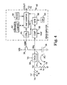
- Figure 1 is a diagram illustrating an exemplary embodiment of a magnetic memory 10.
- the magnetic memory 10 may provide a method of calibrating read circuits which improves the reliability of read operations.
- the magnetic memory cells 14 are arranged in rows and columns, with the rows extending along an x-direction and the columns extending along a y-direction. Only a relatively small number of magnetic memory cells 14 are shown to simplify the description of the invention.
- the array 12 is any suitable size.
- the array 12 may utilize highly parallel modes of operation, such as 64-bit wide or 128-bit wide operation.
- word lines 16 extend along the x-direction in a plane on one side of array 12 and bit lines 18 extend along the y-direction in a plane on an adjacent side of array 12. In one embodiment, there is one word line 16 for each row of array 12 and one bit line 18 for each column of array 12. In the embodiment illustrated in Figure 1 , magnetic memory cell 14 is located at an intersection or cross point of a word line 16 and a bit line 18.
- Magnetic memory cells 14 are not limited to any particular type of device. Magnetic memory cells 14 may be, for example, spin dependent tunneling junction devices, anisotropic magnetoresistance devices, giant magnetoresistance devices, colossal magnetoresistance devices, extraordinary magnetoresistance devices or very large magnetoresistance devices.
- magnetic memory 10 includes a row decoder 28, a read circuit 46 and a write circuit 32.
- Row decoder 28 selects word lines 16 during read and write operations.
- a word line 16 may be selected during a read operation by connecting that word line 16 to ground.
- Read circuit 46 senses the resistance of selected memory cells 14 during read operations.
- the read circuit 46 includes direct injection charge amplifiers 34, digital sense amplifiers 40, reset switches 36 and integrator capacitors 38.
- a memory cell 14 is selected by supplying a row address Ax to the row decoder 28 and a column address Ay to steering circuits 30.
- the row decoder 28 couples a word line 16 to ground.
- a steering circuit 30 couples a bit line 18 to a charge amplifier 34.
- a selected memory cell 14 lies at the cross point of selected word and bit lines 16 and 18.
- Write circuit 32 orients the magnetization of the selected memory cells 14 during write operations.
- the write circuit 32 is not shown in detail in order to simplify the explanation of the invention.
- the direct injection charge amplifier 34 supplies a current to the corresponding integrator capacitor 38 while maintaining a potential on the non-selected memory cells 14 of the selected bit line 18 (see also, Figure 5 ). This potential is equal to the potential applied to non-selected rows and columns of the array 12.
- the digital sense amplifier 40 measures signal integration time. The signal integration time is partly a function of the resistance of the selected memory cell 14, which is either at a first state R or a second state R+ ⁇ R.
- the digital sense amplifier 40 can determine the resistance state of the memory cell 14 and, therefore, the logic value stored in the memory cell 114 by comparing the signal integration time to one or more thresholds.
- An output of the digital sense amplifier 40 is supplied to an output register 42 which, in turn, is coupled to an I/O pad 44 of the magnetic memory 10.
- the read circuit 46 reads out data in m-bit words, whereby the resistance states of a number m of memory cells 14 are sensed simultaneously.
- a first group of k contiguous bit lines 18 can be multiplexed into a first charge amplifier 34
- a second group of k contiguous bit lines 18 can be multiplexed into a second charge amplifier 34, and so on.
- each steering circuit 30 includes a set of switches that connect each bit line 18 to either a constant voltage source or a charge amplifier 34.
- Each steering circuit 30 further includes a column decoder. The column decoder selects only one switch for connecting the selected bit line 18 to the charge amplifier 34. All other (unselected) bit lines 18 are connected to the constant voltage source.
- the constant voltage source is supplied from an external circuit.
- FIGS 2A and 2B are diagrams illustrating parallel and anti-parallel magnetization of a magnetic memory cell.
- magnetic memory cell 14 is a spin dependent tunneling device.
- Magnetic memory cell 14 includes a magnetic layer referred to as data storage layer 20, a magnetic layer referred to as reference layer 22, and a tunnel barrier 24 disposed between data storage layer 20 and reference layer 22.
- Data storage layer 20 is referred to as a free layer because it has a magnetization orientation that is not pinned and which can be oriented in either of two directions along an easy axis which lies in a plane.
- Reference layer 22 is referred to as a pinned layer because it has a magnetization that is oriented in a plane but is fixed so as not to rotate in the presence of an applied magnetic field within a range of interest.
- the magnetization orientation assumes one of two stable orientations at any given time which are the parallel and anti-parallel orientations.
- Figure 2A illustrates by arrows the parallel orientation when the magnetization of the free and pinned layers 20 and 22 are in the same direction along the easy axis
- With parallel orientation the orientation of magnetization in the data storage layer 20 is substantially parallel to the magnetization in the reference layer 22 along the easy axis and magnetic memory cell 14 is in a low resistance state which can be represented by the value R.
- Figure 2B illustrates by arrows the anti-parallel orientation when the magnetization of the free and pinned layers 20 and 22 are in opposite directions.
- anti-parallel orientation the orientation of magnetization in the data storage layer 20 is substantially anti-parallel to the magnetization in the reference layer 22 along the easy axis and magnetic memory cell 14 is in a high resistance state which can be represented by the value R+ ⁇ R.
- the insulating tunnel barrier 24 allows quantum mechanical tunneling to occur between the free and pinned layers 20 and 22. Because the tunneling is electron spin dependent, the resistance of magnetic memory cell 14 is a function of the relative orientations of the magnetization of the free and pinned layers 20 and 22.
- Data is stored in the magnetic memory cell 14 by orienting the magnetization along the easy axis of the free layer 20.
- a logic value of "0" is stored in magnetic memory cell 14 by orienting the magnetization of free layer 20 such that the magnetization orientation is parallel
- a logic value of "1” is stored in magnetic memory cell 14 by orienting the magnetization of free layer 20 such that the magnetization orientation is anti-parallel.
- a logic value of "1” is stored in magnetic memory cell 14 by orienting the magnetization of free layer 20 such that the magnetization orientation is parallel
- a logic value of "0” is stored in magnetic memory cell 14 by orienting the magnetization of free layer 20 such that the magnetization orientation is anti-parallel.
- Figure 3 is a diagram illustrating a magnetic memory cell 14 that has been selected.
- the magnetization in free layer 20 of selected magnetic memory cell 14 is oriented by supplying the currents Ix and Iy to conductors 16 and 18 which cross selected magnetic memory cell 14.
- Supplying the current Ix to word line 16 causes a magnetic field Hy to form around conductor 16
- Supplying the current Iy to bit line 18 causes a magnetic field Hx to form around bit line 18.
- the magnetic fields Hx and Hy in the vicinity of free layer 20 cause the magnetization of free layer 20 to rotate from the parallel orientation to the anti-parallel orientation, or to rotate from the anti-parallel orientation to the parallel orientation.
- a magnetic memory cell 14 is read by applying sense currents to word line 16 and bit line 18.
- Magnetic memory cell 14 will have either a resistance of R or a resistance of R+ ⁇ R, depending on whether the orientation of magnetization of the free and pinned layers 20 and 22 is parallel or anti-parallel as illustrated in Figures 2A and 2B .
- FIG. 4 is a diagram illustrating one embodiment of a sense amplifier 40 during a read operation of a selected memory cell 14.
- Sense amplifier 40 supplies a control signal NSINT which controls whether the reset switch 36 is on (conducting) or off (not conducting).
- the reset switch 36 is a PMOS transistor. In other embodiments, the reset switch 36 can be other types or combinations of transistors.
- VDD supply voltage
- the integrator capacitor 38 is charged as a first current follows a first path P1, wherein the first current is conducted through the reset switch 36 and the selected memory cell 14.
- the selected memory cell 14 is represented by a resistor.
- the sense current (Is) conducted through the selected memory cell 14 is supplied from the integrator capacitor 38.
- the second (sense) current follows a second path P2, and is conducted from the integrator capacitor 38 through the selected memory cell 14.
- the second current includes currents from the selected memory cell 14 and any parasitic currents from the array 12.
- the parasitic currents (Ip) from the array 12 can arise because voltages (Vs') applied to the unselected memory cells 14 (illustrated at 14') are not precisely equal to the applied array voltage (Vs).
- the integrator voltage (Vintg) is greater than the voltage across the selected memory cell 14, the capacitor 38 functions as a linear integrator.
- the direct injection charge amplifier 34 controls a sense voltage Vs' across the memory cells 14 which is independent of the second (sense) current.
- Vs sense voltage
- the direct injection charge amplifier 34 maintains the voltage Vs' across selected memory cell 14 at a value equal to Vs so that the voltage Vs-Vs' across unselected memory cells 14' and therefore the parasitic currents Ip are minimized.
- the current that flows in the direct injection charge amplifier 34 is then directly proportional to the resistance of the selected memory cell 14 without having to make corrections or adjustments for variations in the sense voltage Vs'.
- the direct injection charge amplifier 34 includes a high gain negative feedback amplifier for controlling the selected bit line voltage (that is, the sense voltage Vs') to a set value and minimizing the variance of the sense voltage Vs' over a wide range of sense currents (see also, Figure 5 ).
- the resistance of the memory cell 14 and the capacitance of integrator capacitor 38 determine how quickly the integrator capacitor 38 is discharged after reset switch 36 is opened. All other parameters being equal, the integrator capacitor 38 will discharge more quickly when the memory cell 14 has a resistance of R (for example, a logic "0"), than when the memory cell 12 has a resistance of R+AR (for example, a logic "1").
- the sense amplifier 40 measures the integration time to determine the resistance state of the selected memory cell 14 and, therefore, the logic value stored in the selected memory cell 14.
- the sense amplifier 40 includes a comparator 50 for comparing capacitor voltage Vintg to a DC reference voltage Vref.
- the sense amplifier 40 further includes an N-bit counter 52, a high frequency clock 54 and a gate 56.
- the gate 56 is used to start and stop the clock 54, and the clock 54 causes the counter 52 to increment a counter value at clock frequency.
- the counter value stored in the counter 52 will indicate the amount of time for the voltage Vintg on the integrator capacitor 38 to decay to the reference voltage Vref.
- An N-bit preset register 58 is included which can temporarily store the contents of the counter 52 and which can load the preset register 58 contents into the counter 52.
- the preset register 58 can also be loaded with specific values such as for initialization or for 2's complement addition. In other embodiments, the specific values can be supplied from the I/O pads of magnetic memory 10.
- a controller 60 is included to control the reset switch 36, counter 52, gate 56, preset register 58 and threshold compare logic 62.
- the read circuit 46 can operate under different modes which include read operations and measurement of the calibration values. In other embodiments, the different modes are selected by supplying signals to the I/O pads of magnetic memory 10.
- the negative of a threshold is preloaded into the counter 52.
- the most significant bit of the counter value represents the logic value stored in the selected memory cell 14.
- An output DOUT of the most significant bit of the counter 52 is coupled to the register 42.
- the counter 52 before the read operation is performed, the counter 52 is initialized to a value of zero. After the read operation, the magnitude of the counter value is compared to threshold values representing a logic "0" and a logic "1" to determine the logic value stored in the selected memory cell 14. An output DOUT representing the logic value is coupled to the register 42.
- the calibration value of the read circuit 46 when the calibration value of the read circuit 46 is measured, a read operation is performed and the calibration value corresponds to the counter value stored in counter 52 after a read operation is performed.
- the calibration value corresponds to the amount of time for the voltage Vintg on the integrator capacitor 38 to decay to the reference voltage Vref, wherein the calibration value corresponds to the amount of time.
- the sense amplifier 40 includes threshold compare logic 62.
- the threshold compare logic 62 stores maximum range and minimum range values. In the illustrated embodiment, a large error calibration of the read circuit 46 is performed if a calibration value is within a maximum range. A small error calibration of the read circuit 46 is performed if the calibration value is within a minimum range.
- the maximum range includes a maximum upper threshold value and a maximum lower threshold value.
- the large error calibration of the read circuit is performed if the calibration value is greater than the maximum upper threshold value or less than the maximum lower threshold value.
- the minimum range includes a minimum upper threshold value and a minimum lower threshold value.
- the small error calibration of the read circuit is performed if the calibration value is equal to or greater than the maximum lower threshold value and less than the minimum lower threshold value, or is greater than the minimum upper threshold value and equal to or less than the maximum upper threshold value.
- the large error calibration and the small error calibration both optimize or match the performance of the components which are coupled to selected and unselected rows or columns and which can adversely affect read performance of the read circuit.
- the large error calibration and the small error calibration correct for unintended current leakage resulting from unselected rows which are coupled to selected columns, where the unselected rows are coupled to unselected components such as memory cells which can provide current leakage paths.
- the circuit parameters of magnetic memory 10 are sized to accommodate a sense current range of 200 nA to 500 nA, a power supply voltage VDD of 3.3V, a reference voltage Vref of 1.0 volts, a clock 54 having a clock frequency of 100MHz, and a counter 52 that is 9-bits wide.
- the minimum DC sense current of 200 nA determines the capacitance C of the integrator capacitor 38 for a 2.3V swing (VDD-Vref) in 512 levels, with each clock tick equaling 10 nanoseconds.
- a sense current Is of 400 nA represents a reference logic "1" and a sense current Is of 350 nA represents a reference logic "0".
- a reference logic "1” corresponds to 255 counter ticks (i.e., 0,011,111,111), and a reference logic "0" corresponds to 292 counter ticks (i.e., 0,100,100,100).
- a midpoint counter value corresponds approximately to 273 counter ticks (i.e., 0,100,010,001).
- the maximum lower threshold value, minimum lower threshold value, minimum upper threshold value and the maximum upper threshold value correspond to counter values stored in threshold compare logic 62.
- minimum threshold values are selected to be approximately 2% of the counter value midpoint between a logic "0" and a logic "1" (e.g. 5 counter ticks), and maximum threshold values are selected to be approximately 10% of the counter value midpoint (e.g. 27 counter ticks). In other embodiments, other suitable threshold values can be used.
- the large error calibration of the read circuit for a logic "0" read is performed if the calibration value is greater than a maximum upper threshold value of 300 counter ticks or less than a maximum lower threshold value of 228 counter ticks.
- the small error calibration of the read circuit for a logic "0" read is performed if the calibration value is equal to or greater than a maximum lower threshold value of 228 counter ticks and less than a minimum lower threshold value of 250 counter ticks, or is greater than a minimum upper threshold value of 260 counter ticks and equal to or less than a maximum upper threshold value of 300 counter ticks.
- the large error calibration and the small error calibration are not performed and the read "0" is valid if the calibration value is equal to or greater than 250 counter ticks and equal to or less than 260 counter ticks.
- other suitable values for a valid read and for the maximum lower threshold value, the minimum lower threshold value, the minimum upper threshold value and the maximum upper threshold value can be used.
- the values for a valid read and for the maximum lower threshold value, the minimum lower threshold value, the minimum upper threshold value and the maximum upper threshold value are supplied from the I/O pads of magnetic memory 10.
- the calibration of read circuit 46 can be performed while reading a logic "1".
- the sense amplifier 40 may be disclosed in U.S. Patent No. 6,188,615 to Perner et al., issued February 13, 2001 , entitled "MRAM Device Including Digital Sense Amplifiers''.
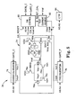
- FIG. 5 is a diagram illustrating one embodiment of a direct injection charge amplifier 34 having digital offset calibration.
- the direct injection charge amplifier 34 includes a large error calibration circuit which is illustrated as a coarse calibration circuit 74, and includes a small error calibration circuit which is illustrated as a fine calibration circuit 76.
- the direct injection charge amplifier 34 includes a PMOS differential amplifier. First, second and third PMOS transistors 78a, 78b and 78e and first and second NMOS transistors 78c and 78d of the differential amplifier provide a controlled current path.
- the substrate is common to the NMOS transistors 78c and 78d.
- the PMOS transistors 78a and 78b are located in isolated n-type wells in the substrate which allow the back gate bias of the first and second PMOS transistors 78a and 78b to be controlled. Arrows extending through gates of the PMOS transistors 78a and 78b schematically represent connections to the substrate.
- the differential amplifier is followed by a second stage amplifier circuit including two transistors 80a and 80b for boosting the gain so that the output can be controlled to a desired value when the feedback loop is closed.
- the feedback loop includes the first PMOS transistor 78a, followed by the second stage operational amplifier circuit 80a and 80b and a current source transistor 86.
- the feedback signal is the output voltage Vout and the loop is closed when the output voltage Vout is applied to the gate of the first PMOS transistor 78a.
- Frequency compensation components controls the stability of the second stage operational amplifier circuit by reducing high frequency gain of the second stage amplifier circuit and thereby preventing the closed loop operational amplifier from going unstable.
- the current source transistor 86 has a gate coupled to an output of circuit 82/84 and a drain to source path coupled to an input of the differential amplifier.
- the direct injection charge amplifier 34 senses and controls the output voltage Vout to a prescribed value by adjusting the current in the current source transistor 86 and then holding the current in the current source transistor 86 constant for a period of time.
- the coarse calibration circuit 74 performs coarse offset correction.
- the coarse calibration circuit 74 performs the coarse correction by applying a back gate bias voltage Vcc+ and Vcc- to the isolated wells of the first and second PMOS transistors 78a and 78b.
- the level of the back gate bias voltage Vcc+ and Vcc- is set according to a first digital number which is stored in the coarse calibration circuit 74.
- the sensitivity of the offset voltage to back gate voltage variations can be rather large. Therefore, applying the back gate bias voltage Vcc+ and Vcc- is better suited for making coarse corrections to the offset voltage.
- the fine calibration circuit 76 performs fine offset correction.
- the fine correction is performed by adjusting impedance of the transistors 78a, 78b, 78c, 78d and 78e in the differential amplifier.
- the amount of the impedance adjustment is determined by a second digital number, which is stored in the fine calibration circuit 76.
- the direct injection charge amplifier 34 may be as disclosed in U.S. Patent No. 6,262,625 to Perner et al., issued July 17, 2001 , entitled “Operational Amplifier with Digital Offset Calibration” .
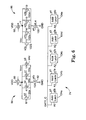
- FIG 6 is a diagram illustrating one embodiment of a coarse calibration circuit 74 for the direct injection charge amplifier 34 illustrated in Figure 5 .
- the coarse calibration circuit 74 includes a pair of programmable voltage dividers 88 and 96 for developing the back gate bias voltage Vcc+ and Vcc- for the isolated wells of the PMOS transistors 78a and 78b. Each voltage divider 88 and 96 is connected between a source of operating potential (VDD) and a reference potential (GND).
- VDD source of operating potential
- GND reference potential
- the first voltage divider 88 is shown, by way of example, as being formed by upper and lower transistors 90 and 92, and four middle transistors 94a, 94b, 94c and 94d having different drain to source path resistances.
- the numbers 1/10, 2/10, 4/10 and 8/10 represent transistor length and width sizes.
- the transistor size variations set the voltage divider ratios. Turning on different combinations of the middle transistors 94a, 94b, 94c and 94d will change the voltage drop Vcc+ between a first node X and ground GND. The voltage drop Vcc+ is applied to the isolated well of the first PMOS transistor 78a.
- the second voltage divider 96 also includes upper and lower transistors 98 and 100, and four middle transistors 102a, 102b, 102c and 102d having different drain to source path resistances. Turning on different combinations of the middle transistors 102a, 102b, 102c and 102d will change the voltage drop Vcc- between a second node Y and ground GND. The voltage drop Vcc- is applied to the isolated well of the second PMOS transistor 78b.
- the middle transistors 94a, 94b, 94c, 94d, 102a, 102b, 102c and 102d are turned on and off according to a first number stored in a first group of address latches 104a, 104b, 104c and 104d.
- the first number determines the back gate bias voltage Vcc+ and Vcc- applied to the isolated wells of the first and second PMOS transistors 78a and 78b.
- a fifth address latch 104e controls the lower transistors 92 and 100 so that either positive or negative correction can be performed.
- the coarse calibration circuit 74 can control the back gate bias voltage Vcc+ and Vcc- to as many as 2 5 different levels.
- FIG 7 is a diagram illustrating one embodiment of a fine calibration circuit 76 for the amplifier illustrated in Figure 5 .
- the fine calibration circuit 76 includes first and second programmable circuits 106 and 108 which combine with the first and second NMOS transistors 78c and 78d, respectively, to form first and second current mirrors.
- the programmable circuit 106 is shown, by way of example, as being formed by a first pair of transistors 110 and 112, and four middle transistors 114a, 114b, 114c and 114d having different drain to source path resistances. Turning on different combinations of the middle transistors 114a, 114b, 114c and 114d will change the impedance levels in the first current mirror.
- the second current mirror 108 is also shown, by way of example, as being formed by a second pair of transistors 116 and 118, and four middle transistors 120a, 120b, 120c and 120d having different drain to source path resistances. Turning on different combinations of the middle transistors 120a, 120b, 120c and 120d will change the impedance level in the second current mirror.
- the middle transistors 114a, 114b, 114c, 114d, 120a, 120b, 120c and 120d are turned on and off according to a second number stored in a second group of static latches 122a, 122b, 122c and 122d.
- the second number determines the impedance of the transistors 78a, 78b, 78c, 78d and 78e in the differential amplifier.
- a fifth latch 122e controls the transistors 112 and 118 so that either positive or negative correction can be performed.
- the fine calibration circuit 76 can control the transistor impedance to as many as 2 5 different levels.
- the direct injection charge amplifier 34 includes a calibration control circuit 90, a test current source 92 and a counter 94 for determining the first and second numbers that should be stored in the coarse and fine calibration circuits 74 and 76.
- the test current source 92 supplies a test current Itest to a node K.
- the magnitude of the test signal current Itest can be selected to be approximately the value of the expected output signal current Iout in the absence of offset error.
- the counter 94 begins counting from zero.
- the count is supplied to the latches 104a to 104e and 122a to 122e of the coarse and fine calibration circuits 74 and 76 via a control bus A0:A5.
- Coarse calibration is performed when the most significant bit A5 of the count is low, and fine calibration is performed when the most significant bit A5 is high.
- the level of the back gate bias voltage Vcc+ and Vcc- is changed. While the back gate bias voltage Vcc+ and Vcc- is being changed, a voltage excursion at the node K is examined.
- the voltage Vtest at the node K is pulled high.
- the test current Itest is less than or equal to the output current Iout, the voltage Vtest at the node K is pulled low.
- the node K goes from high to low or vice-versa, the voltage excursion at the node K is large enough to serve as a logic input to CMOS logic gates in the calibration control circuit 90.
- the number that caused the voltage excursion is held in the latches 104a to 104e of the coarse calibration circuit 74. That number will be used to set the' back gate bias voltage Vcc+ and Vcc-.
- the number that caused the voltage excursion is held in the latches 122a to 122e of the fine calibration circuit 76. That number will be used to set the transistor impedance.
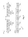
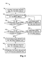
- Figure 8 is a flowchart illustrating an exemplary embodiment of a method of calibrating a read circuit 46.
- the flow chart is illustrated at 130.
- the exemplary method illustrates the calibration of the read circuit 46 in a magnetic memory 10 which includes a first memory cell 14 and a second memory cell 14.
- the method at 132 couples the first memory cell 14 to the read circuit 46.
- the first memory cell 14 is a selected first memory cell 14.
- the selected first memory cell 14 is intersected by a selected word line 16 and a selected bit line 18.
- the selected word line 16 is selected by applying a first potential to the selected word line 16 and the selected bit line 18 is selected by applying a second potential to the selected bit line 18.
- the first potential is a ground potential and the second potential is an array voltage potential.
- the method at 134 measures a calibration value of the read circuit 46.
- the read circuit 46 includes an integrator 38.
- the calibration value is measured by measuring an amount of time for a voltage on integrator 38 to decay to a reference voltage. In this embodiment, the calibration value corresponds to the time.
- the method at 136 determines if the calibration value is within a maximum range.
- the maximum range includes a maximum upper threshold value and a maximum lower threshold value.
- the calibration value is within the maximum range if the calibration value is greater than the maximum upper threshold value or less than the maximum lower threshold value.
- the method at 138 performs a large error calibration of the read circuit 46.
- the large error calibration includes performing a coarse calibration of the direct injection charge amplifier 34 and performing a fine calibration of the direct injection charge amplifier 34.
- the direct injection charge amplifier 34 has at least one transistor in an isolated well.
- Performing the coarse calibration includes first generating a test signal. Next, an input signal is supplied to the direct injection charge amplifier 34. An output signal of the direct injection charge amplifier 34 is compared to the test signal. Next, a back gate bias voltage of the isolated well is adjusted.
- Performing the fine calibration includes adjusting an impedance of the transistor. Next, a number that corresponds to the back gate bias voltage and the transistor impedance that causes the output signal to be within an acceptable limit of the test signal is stored.
- the method at 140 determines if the calibration value is within a minimum range.
- the minimum range includes a minimum upper threshold value and a minimum lower threshold value.
- the calibration value is within the minimum range if the calibration value is equal to or greater than the maximum lower threshold value and less than the minimum lower threshold value, or is greater than the minimum upper threshold value and equal to or less than the maximum upper threshold value.
- the method at 142 performs a small error calibration of the read circuit 46.
- the small error calibration includes performing a fine calibration of the direct injection charge amplifier 34.
- performing the fine calibration includes first generating a test signal. Next, an input signal is supplied to the direct injection charge amplifier 34. An output signal of the direct injection charge amplifier 34 is compared to the test signal. Next, an impedance of one or more transistors is adjusted. Next, a number that corresponds to the transistor impedance that causes the output signal to be within an acceptable limit of the test signal is stored.
- the calibration value of the read circuit 46 is measured at 134. If the calibration value is not within the minimum range, the method at 144 performs a read operation on the first memory cell 14.
- the method at 146 couples the second memory cell 14 to the read circuit 46.
- the second memory cell 14 is a selected second memory cell 14.
- the selected second memory cell 14 is intersected by a selected word line 16 and a selected bit line 18.
- the selected bit line 18 for the selected second memory cell 14 and the selected first memory cell 14 is the same selected bit line 18.
- the selected word line 16 is selected by applying a first potential to the selected word line 16.
- the selected bit line 18 is selected by applying a second potential to the selected bit line 18.
- the first potential is a ground potential and the second potential is an array voltage potential.
- the method at 146 After the second memory cell is coupled to the read circuit, the method at 146 performs a read operation on the second memory cell 14.
- the invention also provides a magnetic random access memory comprising a magnetic memory cell; a read circuit for performing a read operation to the memory cell; a control circuit configured to calibrate the read circuit including measuring a calibration of the magnetic memory cell, and performing a large error calibration if the calibration value is within a maximum range to perform a small error calibration if the calibration value is within a minimum range.
Landscapes
- Engineering & Computer Science (AREA)
- Computer Hardware Design (AREA)
- Mram Or Spin Memory Techniques (AREA)
- For Increasing The Reliability Of Semiconductor Memories (AREA)
- Digital Magnetic Recording (AREA)
Claims (10)
- Procédé d'étalonnage d'un circuit de lecture (46) dans une mémoire magnétique à point de connexion résistant (10), comprenant les étapes séquentielles suivantes :mesure (134) d'une valeur d'étalonnage ;exécution d'un étalonnage d'erreur importante (138) si (136) la valeur d'étalonnage est dans une plage maximale, dans lequel la plage maximale comprend une valeur seuil supérieure maximale et une valeur seuil inférieure maximale, et dans lequel l'étalonnage d'erreur importante est exécuté si la valeur d'étalonnage est supérieure à la valeur seuil supérieure maximale ou inférieure à la valeur seuil inférieure maximale ; etexécution d'un étalonnage d'erreur peu importante (142) si (140) la valeur d'étalonnage est dans la plage minimale, dans lequel la plage minimale comprend une valeur seuil supérieure minimale et une valeur seuil inférieure minimale, et dans lequel l'étalonnage d'erreur peu importante est exécuté si la valeur d'étalonnage est égale ou supérieure à la valeur seuil inférieure maximale et inférieure à la valeur seuil inférieure minimale, ou est supérieure à la valeur seuil supérieure minimale et égale ou inférieure à la valeur seuil supérieure maximale.
- Procédé selon la revendication 1, comprenant la mesure de la valeur d'étalonnage après que l'étalonnage d'erreur importante a été exécuté.
- Procédé selon la revendication 1 ou 2, comprenant la mesure de la valeur d'étalonnage après que l'étalonnage d'erreur peu importante a été exécuté.
- Procédé selon la revendication 1, 2 ou 3, le circuit de lecture comportant un intégrateur (38), dans lequel la mesure de la valeur d'étalonnage comprend :la mesure d'une durée nécessaire pour qu'une tension (Vintg) sur l'intégrateur tombe à une tension de référence (Vref), la valeur d'étalonnage correspondant à la durée.
- Procédé selon l'une quelconque des revendications précédentes, dans lequel l'exécution de l'étalonnage d'erreur importante comprend :l'exécution d'un étalonnage approximatif du circuit de lecture ; etl'exécution d'un étalonnage précis du circuit de lecture.
- Procédé selon l'une quelconque des revendications précédentes, dans lequel l'exécution de l'étalonnage d'erreur peu importante comprend :l'exécution d'un étalonnage précis du circuit de lecture.
- Procédé selon la revendication 1, comprenant l'étape consistant à exécuter soit une première, soit une première et une deuxième opérations de lecture (146) sur la mémoire magnétique.
- Procédé selon l'une quelconque des revendications précédentes, dans lequel la mémoire magnétique (10) comprend un réseau de canaux bits (18) s'étendant dans une première direction qui coupe un réseau de cellules de mémoire (14) et un réseau de canaux mots (16) s'étendant dans une deuxième direction qui coupe le réseau de cellules de mémoire, dans lequel le nombre de canaux mots dans le réseau de canaux mots est égal ou supérieur à M, le procédé comprenant les étapes consistant à :sélectionner, pour (i) égal à un, un canal mot (i) dans le réseau de canaux mots et un canal bit dans le réseau de canaux bits qui coupent une cellule de mémoire (i) dans le réseau de cellules de mémoire ;mesurer la valeur d'étalonnage ;exécuter l'étalonnage d'erreur importante si la valeur d'étalonnage est dans la plage maximale ;exécuter l'étalonnage d'erreur peu importante si la valeur d'étalonnage est dans la plage minimale ;exécuter l'opération de lecture sur une première cellule de mémoire ;pour chaque valeur de (i) pour 2≤i≤M :sélectionner le canal mot (i) dans le réseau de canaux mots et le canal bit dans le réseau de canaux bits qui coupent la cellule de mémoire (i) du réseau de cellules de mémoire ; etexécuter une opération de lecture sur la cellule de mémoire (i).
- Circuit de lecture (46), pour une mémoire magnétique à point de connexion résistant (10), comprenant :un moyen pour mesurer une valeur d'étalonnage ;un moyen pour exécuter un étalonnage d'erreur importante si la valeur d'étalonnage est dans une plage maximale, dans lequel la plage maximale comprend une valeur seuil supérieure maximale et une valeur seuil inférieure maximale, et dans lequel l'étalonnage d'erreur importante est exécuté si la valeur d'étalonnage est supérieure à la valeur seuil supérieure maximale ou inférieure à la valeur seuil inférieure maximale ;un moyen pour exécuter un étalonnage d'erreur peu importante si la valeur d'étalonnage est dans une plage minimale, dans lequel la plage minimale comprend une valeur seuil supérieure minimale et une valeur seuil inférieure minimale, et dans lequel l'étalonnage d'erreur peu importante est exécuté si la valeur d'étalonnage est égale ou supérieure à la valeur seuil inférieure maximale et inférieure à la valeur seuil inférieure minimale, ou est supérieure à la valeur seuil supérieure minimale et égale ou inférieure à la valeur seuil supérieure maximale ;un moyen pour exécuter une première opération de lecture sur une mémoire magnétique.
- Mémoire magnétique à point de connexion résistant, comprenant :un circuit de lecture selon la revendication 9 ; etune cellule de mémoire magnétique à point de connexion résistant.
Applications Claiming Priority (2)
| Application Number | Priority Date | Filing Date | Title |
|---|---|---|---|
| US678322 | 2003-10-03 | ||
| US10/678,322 US6894938B2 (en) | 2003-10-03 | 2003-10-03 | System and method of calibrating a read circuit in a magnetic memory |
Publications (2)
| Publication Number | Publication Date |
|---|---|
| EP1526549A1 EP1526549A1 (fr) | 2005-04-27 |
| EP1526549B1 true EP1526549B1 (fr) | 2008-08-13 |
Family
ID=34393897
Family Applications (1)
| Application Number | Title | Priority Date | Filing Date |
|---|---|---|---|
| EP04255360A Expired - Lifetime EP1526549B1 (fr) | 2003-10-03 | 2004-09-03 | Système et procédé de calibration d'un circuit de lecture d'une mémoire magnétique |
Country Status (4)
| Country | Link |
|---|---|
| US (1) | US6894938B2 (fr) |
| EP (1) | EP1526549B1 (fr) |
| DE (1) | DE602004015697D1 (fr) |
| TW (1) | TWI317127B (fr) |
Families Citing this family (9)
| Publication number | Priority date | Publication date | Assignee | Title |
|---|---|---|---|---|
| KR100988087B1 (ko) * | 2003-11-24 | 2010-10-18 | 삼성전자주식회사 | Mram 특성 분석 장치 및 그 분석 방법 |
| KR100721581B1 (ko) * | 2005-09-29 | 2007-05-23 | 주식회사 하이닉스반도체 | 직렬 입/출력 인터페이스를 가진 멀티 포트 메모리 소자 |
| US7379364B2 (en) * | 2006-10-19 | 2008-05-27 | Unity Semiconductor Corporation | Sensing a signal in a two-terminal memory array having leakage current |
| US7372753B1 (en) * | 2006-10-19 | 2008-05-13 | Unity Semiconductor Corporation | Two-cycle sensing in a two-terminal memory array having leakage current |
| US20090234767A1 (en) * | 2008-03-12 | 2009-09-17 | Steidlmayer J Peter | Cost-based financial product |
| US7719876B2 (en) | 2008-07-31 | 2010-05-18 | Unity Semiconductor Corporation | Preservation circuit and methods to maintain values representing data in one or more layers of memory |
| US7830701B2 (en) * | 2008-09-19 | 2010-11-09 | Unity Semiconductor Corporation | Contemporaneous margin verification and memory access for memory cells in cross point memory arrays |
| US11200297B2 (en) | 2019-06-12 | 2021-12-14 | International Business Machines Corporation | Integrator voltage shifting for improved performance in softmax operation |
| US10839900B1 (en) | 2019-06-12 | 2020-11-17 | International Business Machines Corporation | Parasitic voltage drop compensation in large cross-point arrays |
Family Cites Families (6)
| Publication number | Priority date | Publication date | Assignee | Title |
|---|---|---|---|---|
| US6262625B1 (en) * | 1999-10-29 | 2001-07-17 | Hewlett-Packard Co | Operational amplifier with digital offset calibration |
| US6188615B1 (en) | 1999-10-29 | 2001-02-13 | Hewlett-Packard Company | MRAM device including digital sense amplifiers |
| US6504779B2 (en) * | 2001-05-14 | 2003-01-07 | Hewlett-Packard Company | Resistive cross point memory with on-chip sense amplifier calibration method and apparatus |
| US20030023922A1 (en) * | 2001-07-25 | 2003-01-30 | Davis James A. | Fault tolerant magnetoresistive solid-state storage device |
| US6606262B2 (en) * | 2002-01-10 | 2003-08-12 | Hewlett-Packard Development Company, L.P. | Magnetoresistive random access memory (MRAM) with on-chip automatic determination of optimized write current method and apparatus |
| US7049577B2 (en) * | 2002-09-30 | 2006-05-23 | Teradyne, Inc. | Semiconductor handler interface auto alignment |
-
2003
- 2003-10-03 US US10/678,322 patent/US6894938B2/en not_active Expired - Lifetime
-
2004
- 2004-03-31 TW TW093108849A patent/TWI317127B/zh not_active IP Right Cessation
- 2004-09-03 DE DE602004015697T patent/DE602004015697D1/de not_active Expired - Lifetime
- 2004-09-03 EP EP04255360A patent/EP1526549B1/fr not_active Expired - Lifetime
Also Published As
| Publication number | Publication date |
|---|---|
| US20050073890A1 (en) | 2005-04-07 |
| TW200514081A (en) | 2005-04-16 |
| US6894938B2 (en) | 2005-05-17 |
| DE602004015697D1 (de) | 2008-09-25 |
| EP1526549A1 (fr) | 2005-04-27 |
| TWI317127B (en) | 2009-11-11 |
Similar Documents
| Publication | Publication Date | Title |
|---|---|---|
| US7079436B2 (en) | Resistive cross point memory | |
| US6999366B2 (en) | Magnetic memory including a sense result category between logic states | |
| EP1096501B1 (fr) | Dispositif MRAM avec des amplificateurs de détection | |
| JP4657438B2 (ja) | 演算増幅器 | |
| US6128239A (en) | MRAM device including analog sense amplifiers | |
| US7453719B2 (en) | Magnetic random access memory with improved data reading method | |
| US6256247B1 (en) | Differential sense amplifiers for resistive cross point memory cell arrays | |
| US6259644B1 (en) | Equipotential sense methods for resistive cross point memory cell arrays | |
| US6462979B2 (en) | Integrated memory having memory cells with magnetoresistive storage effect | |
| JP3965373B2 (ja) | 可調整電流モード差動増幅器 | |
| US6385111B2 (en) | Reference signal generation for magnetic random access memory devices | |
| US8284595B2 (en) | Magnetic random access memory and operating method of the same | |
| US20060092689A1 (en) | Reference current source for current sense amplifier and programmable resistor configured with magnetic tunnel junction cells | |
| US6807118B2 (en) | Adjustable offset differential amplifier | |
| US6990030B2 (en) | Magnetic memory having a calibration system | |
| EP1526549B1 (fr) | Système et procédé de calibration d'un circuit de lecture d'une mémoire magnétique | |
| US6834017B2 (en) | Error detection system for an information storage device | |
| US6980455B2 (en) | Remote sensed pre-amplifier for cross-point arrays | |
| US6804145B2 (en) | Memory cell sensing system and method | |
| US7002838B2 (en) | Semiconductor storage device |
Legal Events
| Date | Code | Title | Description |
|---|---|---|---|
| PUAI | Public reference made under article 153(3) epc to a published international application that has entered the european phase |
Free format text: ORIGINAL CODE: 0009012 |
|
| AK | Designated contracting states |
Kind code of ref document: A1 Designated state(s): AT BE BG CH CY CZ DE DK EE ES FI FR GB GR HU IE IT LI LU MC NL PL PT RO SE SI SK TR |
|
| AX | Request for extension of the european patent |
Extension state: AL HR LT LV MK |
|
| 17P | Request for examination filed |
Effective date: 20050822 |
|
| AKX | Designation fees paid |
Designated state(s): DE NL |
|
| RAP1 | Party data changed (applicant data changed or rights of an application transferred) |
Owner name: SAMSUNG ELECTRONICS CO., LTD. |
|
| GRAP | Despatch of communication of intention to grant a patent |
Free format text: ORIGINAL CODE: EPIDOSNIGR1 |
|
| GRAS | Grant fee paid |
Free format text: ORIGINAL CODE: EPIDOSNIGR3 |
|
| GRAA | (expected) grant |
Free format text: ORIGINAL CODE: 0009210 |
|
| AK | Designated contracting states |
Kind code of ref document: B1 Designated state(s): DE NL |
|
| REF | Corresponds to: |
Ref document number: 602004015697 Country of ref document: DE Date of ref document: 20080925 Kind code of ref document: P |
|
| PG25 | Lapsed in a contracting state [announced via postgrant information from national office to epo] |
Ref country code: NL Free format text: LAPSE BECAUSE OF FAILURE TO SUBMIT A TRANSLATION OF THE DESCRIPTION OR TO PAY THE FEE WITHIN THE PRESCRIBED TIME-LIMIT Effective date: 20080813 |
|
| PLBE | No opposition filed within time limit |
Free format text: ORIGINAL CODE: 0009261 |
|
| STAA | Information on the status of an ep patent application or granted ep patent |
Free format text: STATUS: NO OPPOSITION FILED WITHIN TIME LIMIT |
|
| 26N | No opposition filed |
Effective date: 20090514 |
|
| P01 | Opt-out of the competence of the unified patent court (upc) registered |
Effective date: 20230520 |
|
| PGFP | Annual fee paid to national office [announced via postgrant information from national office to epo] |
Ref country code: DE Payment date: 20230726 Year of fee payment: 20 |
|
| REG | Reference to a national code |
Ref country code: DE Ref legal event code: R071 Ref document number: 602004015697 Country of ref document: DE |