EP1530147A1 - Kapazitanzdetektorschaltung - Google Patents
Kapazitanzdetektorschaltung Download PDFInfo
- Publication number
- EP1530147A1 EP1530147A1 EP04256747A EP04256747A EP1530147A1 EP 1530147 A1 EP1530147 A1 EP 1530147A1 EP 04256747 A EP04256747 A EP 04256747A EP 04256747 A EP04256747 A EP 04256747A EP 1530147 A1 EP1530147 A1 EP 1530147A1
- Authority
- EP
- European Patent Office
- Prior art keywords
- row
- line
- capacitance
- voltage
- column
- Prior art date
- Legal status (The legal status is an assumption and is not a legal conclusion. Google has not performed a legal analysis and makes no representation as to the accuracy of the status listed.)
- Granted
Links
Images



Classifications
-
- G—PHYSICS
- G06—COMPUTING OR CALCULATING; COUNTING
- G06F—ELECTRIC DIGITAL DATA PROCESSING
- G06F3/00—Input arrangements for transferring data to be processed into a form capable of being handled by the computer; Output arrangements for transferring data from processing unit to output unit, e.g. interface arrangements
- G06F3/01—Input arrangements or combined input and output arrangements for interaction between user and computer
- G06F3/03—Arrangements for converting the position or the displacement of a member into a coded form
- G06F3/041—Digitisers, e.g. for touch screens or touch pads, characterised by the transducing means
- G06F3/0416—Control or interface arrangements specially adapted for digitisers
- G06F3/0418—Control or interface arrangements specially adapted for digitisers for error correction or compensation, e.g. based on parallax, calibration or alignment
- G06F3/04182—Filtering of noise external to the device and not generated by digitiser components
-
- G—PHYSICS
- G06—COMPUTING OR CALCULATING; COUNTING
- G06V—IMAGE OR VIDEO RECOGNITION OR UNDERSTANDING
- G06V40/00—Recognition of biometric, human-related or animal-related patterns in image or video data
- G06V40/10—Human or animal bodies, e.g. vehicle occupants or pedestrians; Body parts, e.g. hands
- G06V40/12—Fingerprints or palmprints
- G06V40/13—Sensors therefor
- G06V40/1306—Sensors therefor non-optical, e.g. ultrasonic or capacitive sensing
-
- G—PHYSICS
- G06—COMPUTING OR CALCULATING; COUNTING
- G06F—ELECTRIC DIGITAL DATA PROCESSING
- G06F3/00—Input arrangements for transferring data to be processed into a form capable of being handled by the computer; Output arrangements for transferring data from processing unit to output unit, e.g. interface arrangements
- G06F3/01—Input arrangements or combined input and output arrangements for interaction between user and computer
- G06F3/03—Arrangements for converting the position or the displacement of a member into a coded form
- G06F3/041—Digitisers, e.g. for touch screens or touch pads, characterised by the transducing means
- G06F3/044—Digitisers, e.g. for touch screens or touch pads, characterised by the transducing means by capacitive means
- G06F3/0446—Digitisers, e.g. for touch screens or touch pads, characterised by the transducing means by capacitive means using a grid-like structure of electrodes in at least two directions, e.g. using row and column electrodes
Definitions
- the present invention relates to a capacitance detecting circuit and detecting method for detecting a small capacitance, and to a fingerprint sensor employing the same.
- a pressure-sensitive capacitance sensor of a type in which column lines and row lines are formed at a predetermined pitch on surfaces of two films, respectively, the films being disposed opposing each other via an insulating film or the like with a predetermined gap provided therebetween has been developed.
- the pressure-sensitive capacitance sensor when a finger is placed, the shapes of the films change according to the ridges and valleys of the fingerprint, and the gap between the column lines and the row lines change according to the change in the shapes of the films.
- the form of the fingerprint is detected as small changes in capacitances at the intersections of the column lines and the row lines.
- a capacitance detecting circuit of the type described above adjacent detecting lines of capacitors (sensor elements) are respectively connected to a non-inverting input terminal and an inverting input terminal of a differential amplifier circuit, and the difference between voltage values of detection signals of the detecting lines is amplified, so that noise superposed on the detection signals is cancelled to a certain extent, suppressing the effect of the noise.
- a circuit is disclosed, for example, in Japanese Unexamined Patent Application Publication No. 11-118415 paragraphs [0011] to [0064] and Fig. 2).
- the capacitance detecting circuit at a plurality of small capacitors (sensor elements) disposed on a row-by-row basis, the small capacitors are charged and discharged by a charge amp circuit, and differential detection is carried out for adjacent small capacitances on each row.
- the measurement techniques for differential detection can be applied to a capacitance detecting circuit of a sensor in which column lines and row lines cross each other and sensor elements are disposed in a matrix shape. Measurement signals of adjacent row lines are input to a non-inverting input terminal and an inverting input terminal of a differential amplifier to detect a differential component of charging or discharging associated with a driving pulse of a column line, so that reduction in noise due to crosstalk between row lines is expected.
- the arrangement is such that a difference in voltage or current based on capacitances of adjacent sensor elements is detected.
- the conventional capacitance detecting circuit lacks a reference for a subject of measurement, the level of a detection signal is determined by capacitances of adjacent detection lines, so that uniform detection is inhibited even in a single row. Thus, the mutual effect of the detecting lines is not fully eliminated, causing degradation in the resolution of detecting capacitance by the sensor elements.
- the conventional capacitance detecting circuit has the drawback that it is not possible to obtain uniformly precise measurement results over the entire surface of a two-dimensional sensor such as an area sensor.
- the present invention has been made in view of the situation described above, and an object thereof is to provide a capacitance detecting circuit and detecting method and a fingerprint sensor employing the same with which the effect of external noise is suppressed to improve S/N ratio, allowing detection at a sufficient sensitivity of a small capacitance Cs and a capacitance change ⁇ Cs of the capacitance Cs at an intersection (sensor element) of a column line and a row line.
- the present invention in one aspect thereof, provides a capacitance detecting circuit for detecting, in terms of voltage, change in capacitance at intersections of a plurality of column lines and a plurality of row lines crossing each other.
- the capacitance detecting circuit includes a column-line driving unit for driving a column line; a row-line selector for selecting a specific row line from the plurality of row lines; and a capacitance calculator for calculating a capacitance at an intersection of the specific row line and the driven column line based on a reference current that flows in relation to a reference capacitance and a current that flows in relation to the capacitance at the intersection.
- the row-line selector selects a first row line and a second row line adjacent to each other
- the capacitance calculator includes a differential-voltage outputting unit for amplifying a difference between values of currents corresponding to capacitances at respective intersections associated with the first and second row lines, and outputting the amplified difference as a differential voltage signal; and a calculator for calculating values of voltages corresponding to the capacitances at the respective intersections based on differential voltage signals sequentially input to the calculator.
- the row-line selector in a first detecting period, selects a line connected to the reference capacitance as a first row line, and a row line adjacent to the first row line as a second row line, the row-line selector, in and after a second detecting period, selects row lines adjacent to each other from the plurality of row lines as first and second row lines, and the calculator cumulatively adds differential voltage signals sequentially input thereto, thereby obtaining voltage values corresponding to capacitances at intersections.
- the row-line selector in and after the second detecting period, sequentially selects row lines adjacent to each other as first and second row lines, successively to the first and second row lines selected in the first detecting period.
- a difference value between measured voltages relating to the reference capacitor and a row line adjacent to the reference capacitor is obtained by a differential amplifier, then a difference between measured voltages relating to the first row line and a second row line adjacent to the first row line is obtained, and so forth, thereby sequentially determining difference values between measured voltages of each pair of adjacent row lines, and the difference values are cumulatively added.
- measured voltages relating to the respective row lines can be readily obtained by a simple calculation from a voltage value corresponding to the reference capacitance and voltage sums at the respective iterations of cumulative addition.
- noise superposed on detection signals of detecting lines can be removed.
- the plurality of row lines is divided into row-line groups, the row-line selector and the differential-voltage outputting unit are provided individually for each of the row-line groups, and the calculator calculates values of voltages corresponding to the capacitances at the intersections individually for each of the row-line groups.
- the column-line driving unit outputs a signal that rises to a first voltage and then falls to a second voltage to the column line, and when the column line is driven by the first voltage, the differential-voltage outputting unit outputs a third voltage corresponding to a current that charges the capacitances at the intersections, and when the column line is driven by the second voltage, the differential-voltage outputting unit outputs a fourth voltage corresponding to a current that discharges the capacitances at the intersections.
- the row-line selector selects, as the specific row line, a row line connected to an intersection that is a subject of measurement
- the capacitance calculator includes a row-voltage outputting unit for converting a value of a current that flows in relation to a capacitance at the intersection into a value of a measured voltage, and outputting the value of the measured voltage; a reference-row-line selector for selecting row lines other than the specific row line; a reference-voltage generator for converting a value of a current that flows in relation to a reference capacitance into a value of a reference voltage, the reference capacitance being a sum of capacitances at a plurality of intersections of the other row lines and a driven column line, and for outputting the value of the reference voltage; and a calculator for amplifying a difference between the value of the measured voltage and the value of the reference voltage to calculate a value of a voltage corresponding to the capacitance at the intersection.
- a sum of intersections of a driven column line and other row lines in the matrix is used as a reference capacitance against small change in capacitance at an intersection of the column line and a row line.
- an amplification factor of the reference-voltage generator is controlled to be substantially 1/(n - 1) of an amplification factor of the row-voltage outputting unit, where n denotes the number of the row lines other than the specific row line.
- a sum of intersections with other row lines in the matrix is used as a reference capacitance, by adjusting the magnitude of the reference capacitance and the level of noise component to values suitable for the capacitance at a subject intersection for detection, noise superposed on signals of the row lines due to crosstalk or the like can be removed more precisely.
- the present invention in another aspect thereof, provides a fingerprint sensor including the capacitance detecting circuit described above.
- a fingerprint sensor including the capacitance detecting circuit described above.
- the present invention in another aspect thereof, provides a capacitance detecting method for detecting, in terms of voltage, change in capacitance at intersections of a plurality of column lines and a plurality of row lines crossing each other.
- the capacitance detecting method includes a column-line driving step of driving a column line; a row-line selecting step of selecting a specific row line from the plurality of row lines; and a capacitance calculating step of calculating a capacitance at an intersection of the specific row line and the driven column line based on a reference current that flows in relation to a reference capacitance and a current that flows in relation to the capacitance at the intersection.
- a capacitance detecting circuit of the present invention an arrangement for removing noise of the same phase in a differential amplifier circuit and an arrangement for separating capacitances at respective intersections of a driven column line and row lines based on cumulative values of difference between each pair of adjacent row lines are both provided, so that a high resolution is achieved. Furthermore, since temporal differential amplification calculations involving rising and falling of column lines are combined, advantageously, it is possible to detect, at a high precision, a small capacitance at an intersection of a row line and a column line, or an amount of change in capacitance at an intersection.
- a capacitance detecting circuit of the present invention for example, when a fingerprint is detected, in order to remove noise component input from a human body or the like, instead of detection based on difference between adjacent row lines, a reference for calculating a difference value with outputs of the row lines (detecting lines) is provided separately from the row lines.
- a reference for calculating a difference value with outputs of the row lines is provided separately from the row lines.
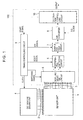
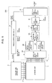
- FIG. 1 is a block diagram showing an example configuration of a capacitance detecting circuit according to the first embodiment.
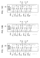
- a plurality of column lines of a column-line set 2 and a plurality of row lines of a row-line set 3 cross each other in a matrix form, the respective intersections forming sensor elements (sensor elements 55 in Fig. 4).
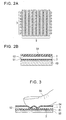
- Fig. 2A is a plan view of the sensor unit 1, and Fig. 2B is a sectional view thereof.
- the row-line set 3 including the plurality of row lines is disposed on a substrate 50.
- an insulating film 51 is laminated, a film 54 is provided over a surface of the insulating film 51 with a gap 52, and the column-line set 2 including the plurality of column lines is attached on a lower surface of the film 54.
- sensor elements are formed as capacitors having a predetermined capacitance via the gap 52 and the insulating film 51.
- Fig. 4 is a schematic diagram showing the matrix of capacitors (sensor elements) between the column lines and the row lines of the sensor unit 1.
- the sensor unit 1 includes a matrix of sensor elements 55, 55, ... , and is connected to a column-line driving unit 4 and a capacitance detecting circuit 100 via the column lines and the row lines, respectively. That is, the column-line set 2 controlled by the column-line driving unit 4 and the row-line set 3 leading to a row-line selector 5 cross each other, the intersections forming the sensor elements 55.
- the column-line driving unit 4 generates a driving pulse to be applied to the column lines, and supplies the driving pulse to a column line of the column-line set.
- the capacitance detecting circuit 100 includes a differential detecting circuit 6, a sample and hold circuit 7, the row-line selector circuit 5, an A/D converter 8, a calculation controlling circuit 10, and a timing controlling circuit 9.
- the capacitance detecting circuit 100 will now be described.
- the row-line selector circuit 5 selects two row lines from the row-line set 3, and connects the selected row lines respectively to a non-inverting input terminal and an inverting input terminal of the differential detecting circuit 6.
- the differential detecting circuit 6 converts currents into voltages, the currents being based on charges charged to or discharged from the capacitors at the intersections relevant to measurement, and detects a difference value between the non-inverting input terminal and the input terminal, outputting the difference value as a differential signal.
- S/H sample and hold
- the A/D converter 8 in synchronization with an A/D clock input from the calculation controlling circuit 10, converts the voltage level held and output by the sample and hold circuit 7 into a digital value, outputting the digital value to the calculation controlling circuit 10.
- the row-line selector circuit 5 is configured, for example, as shown in Fig. 5.
- a reference capacitor R0 shown in Fig. 5 is a capacitive load whose accurate capacitance Cref is known and that serves as a reference for measurement of capacitances at intersections.
- the value of the reference capacitor R0 is chosen to be approximate (similar) to that of a row line.
- the row-line selector circuit 5 includes a switch SW0 connected to the reference capacitor R0, and switches SW1, SW2, SW3, SW4, ... respectively associated with row lines R1, R2, R3, R4, ... of the row-line set 3.
- An output terminal S1 is connected to a negative input terminal IN(-) of the differential detecting circuit 6, and an output terminal S2 is connected to a positive input terminal IN(+) of the differential detecting circuit 6.
- the switch SW0 performs switching as to whether the reference capacitor R0 is to be connected to the output terminal S1 (a connected state) or to be floated (a disconnected state).
- the switches SW1, SW2, SW3, SW4, ... respectively perform switching as to whether the row lines R1, R2, R3, R4, ... are to be floated, to be connected to the output terminal S1, or to be connected to the output terminal S2.
- the timing controlling circuit 9 outputs to the row-line selector circuit 5 such switching signals that cause pairs of adjacent two row lines to be sequentially selected from the row lines of the row-line set 3 (as a pair of row lines to be measured), and that cause the respective switches SW0, SW1, SW2, SW3, SW4, ... to be sequentially connected to one of the output terminal S1 and the output terminal S2.
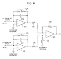
- Fig. 6 is a block diagram showing an example configuration of the differential detecting circuit 6.
- the differential detecting circuit 6 includes differential amplifiers 121, 122, and 123.
- the differential detecting circuit 6 converts currents into voltages, the currents respectively flowing in relation to capacitances at intersections and being input from the input terminals IN(-) and IN(+), and outputs a difference value between the voltages.
- An inverting input terminal of the differential amplifier 121 is connected to an input terminal IN(-), an inverting input terminal of the differential amplifier 122 is connected to an input terminal IN(+), and a predetermined reference potential is supplied to non-inverting input terminals of the differential amplifiers 121 and 122.
- the differential amplifier 121 converts a current input from the input terminal IN(-) into a voltage. Between the inverting input terminal and output terminal thereof, a feedback capacitor 125 and an analog switch 124 for discharging the feedback capacitor 125 are connected in parallel.
- the differential amplifier 122 converts a current input from the input terminal IN(+) into a voltage.
- a feedback capacitor 127 and an analog switch 126 for discharging the feedback capacitor 127 are connected in parallel.
- the capacitor 125 and the capacitor 127 have the same capacitance Cf.
- the output terminal of the differential amplifier 121 is connected to the inverting input terminal of the differential amplifier 123 via a resistor 128.
- the output terminal of the differential amplifier 122 is connected to the non-inverting input terminal of the differential amplifier 123 via a resistor 129.
- the non-inverting input terminal of the differential amplifier 123 is connected to the reference potential via a resistor 130, and the inverting input terminal of the differential amplifier 123 is connected to the output terminal via a resistor 131.
- the differential amplifier 123 amplifies a difference value between output voltages of the differential amplifier 121 and the differential amplifier 122, by an amplification factor determined by the resistors 128, 129, 130, and 131.
- a signal for starting detection of capacitance i.e., a signal for sampling a fingerprint by the fingerprint sensor (the sensor unit 1), is input from outside to the calculation controlling circuit 10.
- the calculation controlling circuit 10 outputs a start signal requesting a start of detection to the timing controlling circuit 9. Then, the timing controlling circuit 9 sequentially outputs switching signals to the row-line selector circuit 5.
- the row-line selector circuit 5 sequentially switches the internal switches according to the switching signals sequentially input (correspondingly to measurements started from the respective timings).
- the timing controlling circuit 9 outputs to the row-line selector circuit 5 such switching signals that cause the reference capacitor R0 having the known capacitance Cref to be connected to the output terminal S1 by the switch SW0, that cause the row line R1 to be connected to the output terminal S2 by the switch SW1, and that cause the other switches SW3, SW4, ... to be floated.
- the row-line selector circuit 5 connects the reference capacitor R0 to the output terminal S1 by the switch SW0, connects the row line R1 to the output terminal S2 by the switch SW1, and causes the other switches SW3, SW4, ... to be floated.
- the timing controlling circuit 9 supplies a reset signal to the differential detecting circuit 6 and the column-line driving unit 4 to initialize the differential detecting circuit 6 and the column-line driving unit 4, making initial setting so that the potentials of the reference capacitor R0 and the row line R1. are equalized and so that the column-line driving unit 4 outputs a driving pulse to the column line C1 of the column-line set 2 in synchronization with the clock input.
- the column-line set 2 includes a plurality of column lines C1, C2, ..., which are sequentially selected in measurement so that driving pulses are output thereto.
- the timing controlling circuit 9 outputs a clock to the column-line driving unit 4 so that the column-line driving unit 4 outputs a driving pulse for driving a column line (causes the driving pulse to rise to H level).
- the column-line driving unit 4 outputs a driving pulse to the column line C1 of the column-line set 2 in synchronization with the clock.
- the differential detecting circuit 6 based on the voltage level of the driving pulse applied, converts currents into voltages, the currents respectively flowing into the input terminals IN(-) and IN(+) in relation to the reference capacitor R0 and the capacitor at the intersection of the column line C1 and the row line R1, and calculates a difference value between the voltages, outputting the difference value as a measured voltage.
- the timing controlling circuit 9 outputs a sample and hold (S/H) signal to the sample and hold circuit 7 after a predetermined time elapses since the application of the driving pulse.
- the sample and hold circuit 7 in synchronization with the sample and hold signal input thereto, temporarily holds the voltage level being output by the differential detecting circuit 6 (stores the voltage level as voltage information), and outputs a signal of the same voltage level to the A/D converter 8.
- the column-line driving unit 4 stops output of the driving pulse (causes the driving pulse to fall to L level) in synchronization with the sample and hold signal.
- the timing controlling circuit 9 after a predetermined time elapses since the output of the sample and hold signal, outputs a conversion signal to the calculation controlling circuit 10.
- the calculation controlling circuit 10 outputs an A/D clock to the A/D converter 8 in synchronization with the conversion signal.
- the A/D converter 8 in synchronization with the A/D clock, converts the voltage level being input from the sample and hold circuit 7 into digital measurement data, outputting the measurement data to the calculation controlling circuit 10.
- V1 denotes the value of a voltage obtained by converting a current that flows through the row line R1 and that is input to the input terminal IN(+)
- Vref denotes the value of a voltage obtained by converting a current that flows through the reference capacitor
- Vofs denotes an offset value for representing output data as an unsigned 8-bit value (the number of bits is arbitrary).
- the timing controlling circuit 9 outputs to the row-line selector circuit 5 such switching signals that cause the row line R1 to be connected to the output terminal S1 by the switch SW1, that cause the row line R2 to be connected to the output terminal S2 by the switch SW2, and that cause the other switches SW0, SW3, SW4, ... to be floated.
- the row-line selector circuit 5 connects the row line R1 to the output terminal S1 by the switch SW1, connects the row line R2 to the output terminal S2 by the switch SW2, and causes the other switches SW0, SW3, SW4, ... to be floated.
- the timing controlling circuit 9 supplies a reset signal to the differential detecting circuit 6 to initialize the differential detecting circuit 6 so that the potentials of the row lines R1 and R2 are equalized.
- the timing controlling circuit 9 outputs a clock to the column-line driving unit 4 so that the column-line driving unit 4 outputs a driving pulse.
- the column-line driving unit 4 outputs a driving pulse to the column line C1 of the column-line set 2 in synchronization with the clock.
- the differential detecting circuit 6 based on the voltage level of the driving pulse applied, converts currents into voltages, the currents respectively flowing into the input terminals IN(-) and IN(+) in relation to the capacitance at the intersection of the column line C1 and the row line R1 and the capacitance at the intersection of the column line C1 and the row line R2, and calculates a difference value between the voltages, outputting the difference value as a measured voltage.
- the timing controlling circuit 9 outputs a sample and hold signal to the sample and hold circuit 7 after a predetermined time elapses since the application of the driving pulse.
- the sample and hold circuit 7 in synchronization with the sample and hold signal input thereto, temporarily holds the voltage level being output from the differential detecting circuit 6, and outputs a signal of the same voltage level to the A/D converter 8.
- the column-line driving unit 4 stops output of the driving pulse in synchronization with the sample and hold signal.
- the timing controlling circuit 9 outputs a conversion signal to the calculation controlling circuit 10 after a predetermined time elapses since the output of the sample and hold signal.
- the calculation controlling circuit 10 outputs an A/D clock to the A/D converter 8 in synchronization with the conversion signal.
- the A/D converter 8 in synchronization with the A/D clock, converts the voltage level being input from the sample and hold circuit 7 into digital measurement data, outputting the measurement data to the calculation controlling circuit 10.
- the timing controlling circuit 9 outputs to the row-line selector circuit 5 such switching signals that cause the row line R2 to be connected to the output terminal S1 by the switch SW2, that cause the row line R3 to be connected to the output terminal S2 by the switch SW3, and that cause the other switches SW0, SW1, SW4 , ... to be floated.
- the row-line selector circuit 5 connects the row line R2 to the output terminal S1 by the switch SW2, connects the row line R3 to the output terminal S2 by the switch S3, and causes the other switches SW0, SW1, SW4, ... to be floated.
- the timing controlling circuit 9 supplies a reset signal to the differential detecting circuit 6 to initialize the differential detecting circuit 6 so that the potentials of the row lines R2 and R3 are equalized.
- the subsequent process is the same as the measurement process for time t2 except in that the pair of adjacent row lines selected for measurement is the row lines R2 and R3.
- the A/D converter 8 in synchronization with the A/D clock, converts the voltage level being input from the sample and hold circuit 7 into digital measurement data, outputting the measurement data to the calculation controlling circuit 10.
- the process described above is carried out until measurement is carried out for all the pairs of the row lines of the row-line set 3. That is, assuming that the row-line set 3 consists of n row lines R1 to Rn, measurement is started with a row-line pair of the reference capacitor R0 and the row line R1, and is continued until a row-line pair of the row line Rn-1 and the row line Rn, with the column line C1 activated by a driving pulse in measurement of each pair of row lines.
- measurement data d1 to dn corresponding to the capacitances at the respective intersections of the column line C1 and the row lines R1 to Rn are stored in relation to the column line C1.
- the process described above is also executed for the other column lines C2 to C15 of the column-line set 2, carrying out measurement for pairs of adjacent row lines among the reference capacitor R0 and the row lines R1 to Rn to obtain measurement data associated with the respective column lines, which is stored in the calculation controlling circuit 10 in relation to the respective column lines.
- the row-line selector circuit 5 When all the pairs of adjacent row lines among the reference capacitor R0 and the row lines R1 to Rn have been formed, i.e., when the row-line pair of the row line Rn-1 and Rn has been formed, the row-line selector circuit 5 outputs a signal indicating an end of row-line pairs to the timing controlling circuit 9.
- the timing controlling circuit 9 Upon receiving input of the signal indicating the end of row-line pairs, the timing controlling circuit 9, before a next clock for the column-line driving unit 4, outputs a control signal to the column-line driving unit 4 so that the column-line driving unit 4 will subsequently output a driving pulse to the column line C2.
- the timing controlling circuit 9 upon receiving a next clock, changes the combination of row-line pair among the row-line set 3 in synchronization with the clock, and outputs a driving pulse to the column line C2, similarly to the case of driving the column line C1, to measure capacitances at the respective intersections of the column line C1 and the row lines.
- the calculation controlling circuit 10 sequentially drives all the column lines of the column-line set 2, and calculates voltage data corresponding to capacitances at the respective intersections from measurement data obtained when measurement of capacitances has been finished for the reference capacitor and the pairs of row lines of the row-line set 3.
- the calculation controlling circuit 10 cumulatively adds measurement data obtained, individually for each of the column lines, thereby obtaining voltage data corresponding to capacitances at the respective intersections of the column lines and the row lines.
- the calculation controlling circuit 10 carries out calculation regarding capacitances at the respective intersections of the column line C1 and the row lines.
- voltage data corresponding to the reference capacitance Cref be denoted as dr (i.e., Vref), measurement data corresponding to the capacitance at the intersection of the column line C1 and the row line R1 as d1 (measurement data at time t1, i.e., measurement data in a measurement that starts at time t1), and voltage data associated with the subject intersection as ds1.
- capacitance is measured only in rising periods of driving pulses (transition from a second voltage to a first voltage, the first voltage being larger than the second voltage) in the measurement described above
- measurement may be carried out both in rising periods and falling periods (transition from the first voltage to the second voltage) of driving pulses so that unneeded offset is removed by temporal differential calculation, serving to improve precision of calculation.
- an offset Vk caused by a feed through current of the analog switch 124 (or 126) is generated in the positive direction when the output OUT decreases or increases from the reference potential, as shown in Fig. 7.
- Fig. 7 is a waveform chart showing an operation of the differential amplifier 121 (or 122).
- Vuref0 -Vuref + Vka
- Vuref Vuref0 + Vka
- a voltage Vd1 at the time of discharging the capacitor Cs to be detected is measured.
- Vd10 the voltage that is proportional to the capacitance Cs
- Vdref0 Vdref - Vka
- a voltage vdl at the time of discharging the capacitor Cs to be detected is also measured.
- Vd10 Vd - Vkb
- Vd1 Vd10 + Vkb
- the differential detecting circuit 6 operates so that: where Vof denotes an offset component of the A/D converter 8.
- the differential detecting circuit 6 operates so that:
- the measured voltages Vsu1 and Vsd1 are sequentially held by the sample and hold circuit 7, and the voltages are then A/D (analog/digital) converted by the A/D converter 8 into measurement data dsu1 and dsd1, respectively, which are stored in a memory of the calculation controlling circuit 10.
- the calculation controlling circuit 10 carries out the following calculation:
- measurement data d not including an offset error caused by a feed through current or an offset Vof caused during conversion by the A/D converter 8 is obtained.
- Vofs denotes an offset value for filling output data by an unsigned 8-bit value (the number of bits is arbitrary)).
- the capacitance detecting circuit 100 temporarily holds measurement data obtained by detection, and carries out calculation for obtaining voltage data corresponding to the capacitances at the respective intersections of the sensor unit 1 after completion of measurement of capacitance for all the column lines.
- the capacitance detecting circuit 100 may cumulatively add measurement data as soon as the measurement data is obtained and carry out calculation for obtaining voltage data concurrently (substantially simultaneously) with the operation for detecting capacitance.
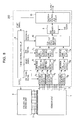
- Fig. 8 is a block diagram showing an example configuration of the capacitance detecting circuit according to the second embodiment.
- parts corresponding to those of the capacitor detecting circuit 100 according to the first embodiment shown in Fig. 1 are designated by the same numerals, and descriptions thereof will be omitted.
- a capacitor detecting circuit 200 shown in Fig. 8 differs from the first embodiment shown in Fig. 1 in that the row-line selector 5 is divided into M row-line selectors 51 to 5M.
- the row lines R1 to Rn of the row-line set 3 are divided into M groups, and the row-line selectors 51 to 5M are respectively associated with row-line groups to be controlled, each consisting of n/M row lines.
- the row-line selectors 51 to 5M are respectively associated with differential detecting circuits 61, 62, ... 6M, and sample and hold circuits 71 to 7M.
- a subsequent-stage selector circuit 11 carries out switching as to which of the voltages levels held by the sample and hold circuits 71 to 7M is to be converted (A/D converted) into digital data.
- the timing controlling circuit 9 outputs a switching signal to the subsequent-stage selector circuit 11 according to the switching of the row-line selector circuits 51 to 5M.
- the same measurements as in the first embodiment i.e., the measurement of a difference value between voltages associated with the reference capacitor R0 and a row-line pair, and measurement of a difference value between.each pair of adjacent row lines in each of the row-line selectors, are carried out individually for each of the row-line selectors 51 to 5M.
- the timing controlling circuit 9 in addition to the switching signal for allowing the respective row-line selectors 51 to 5M to select row-line pairs, outputs switching signals for switching to a next row-line group of each of the row-line selectors when measurement of capacitance for all the row lines of a row-line group of the row-line selector has been finished.
- the capacitor detecting circuit 100 may temporarily hold measurement data obtained by the process described above, carrying out calculation for obtaining voltage data corresponding to the capacitances at the respective intersections of the sensor unit 1 after the measurement of capacitance has been finished for all the column lines.
- the capacitance detecting circuit 100 may cumulatively add measurement data as the measurement data is obtained, carrying out calculation for obtaining voltage data concurrently (substantially simultaneously) with the operation for detecting capacitance.
- the calculation controlling circuit 10 obtains voltage data corresponding to the capacitances at the respective intersections by cumulative addition.
- cumulative addition is carried out individually by each of the row-line selectors, the number of iterations of the cumulative addition is reduced to 1/M compared with the first embodiment (compared with the case where the number of iterations for each column-line group is the entire row-line set 3), so that the accumulation of error is reduced.
- the number of row lines connected to the input terminal IN(+) and IN(-) of the differential amplifiers 61 to 6M is reduced by reconfiguration as row-line groups, so that improvement in the response speed and detection sensitivity of the differential detecting circuit 6 is expected.
- FIG. 9 is a block diagram showing an example configuration of the capacitance detecting circuit according to the third embodiment.
- parts corresponding to those of the capacitance detecting circuit 100 according to the first embodiment shown in Fig. 1 will be designated by the same numerals, and descriptions thereof will be omitted.
- a capacitance detecting circuit 300 shown in Fig. 9 differs from the first embodiment shown in Fig. 1.
- the third embodiment in that as opposed to the first embodiment in which the reference capacitor R0 is provided to serve as a reference measurement voltage and is used as reference data for cumulative addition of measurement data, in the third embodiment, no special reference capacitor is provided, and row lines other than a subject row line for measurement in the row-line set 3 are connected to form a reference capacitor, so that the sum of capacitances of the row lines, i.e., the sum (combined value) of currents that flow through the respective row lines, is used as the value of a current that serves as the reference capacitor (a capacitor that serves as a reference), using the value for calculating capacitances of the row lines. This is based on the fact that averaging the values of current that flow through a plurality of row lines yields a substantially constant value.
- the row-line selector circuit 5A includes switches SSW1 to SSW5, ... that are controlled by the timing controlling circuit 9, and connects each of the row lines of the row-line set 3 to one of the output terminals S1 and S2.
- switches SSW1 to SSW5, ... are controlled by the timing controlling circuit 9 and are associated with the row lines R1 to R5, ... respectively, and connect the respective row lines to one of the output terminals S1 and S2.
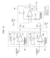
- the configuration of the differential detecting circuit 6 (in the first embodiment) shown in Fig. 6 and the configuration of a differential detecting circuit 6A and C-V converting circuits 6B and 6C shown in Fig. 11 are similar, the configurations differ with respect to the relationship between the capacitance of the capacitor 150 that serves as a feedback capacitor for the differential amplifier 121 and the capacitance of the capacitor 127 that serves as a feedback capacitor for the differential amplifier 122.
- parts corresponding to those in Fig. 6 are designated by the same numerals, and descriptions thereof will be omitted.
- the initial-stage C-V converting circuit 6B corresponds to a converting circuit connected to the input terminal IN(-) of the differential detecting circuit 6 shown in Fig. 6, and the initial-stage C-V converting circuit 6C corresponds to a converting circuit connected to the input terminal IN(+) of the differential detecting circuit 6 shown in Fig. 6.
- the capacitance Cfr of the capacitor 150 is chosen so that: Cfr ⁇ (n - 1) ⁇ Cf
- increase in the voltage associated with the capacitor 150, caused by summing (n - 1) currents is adjusted to be a value equivalent to the voltage level of the capacitor 127, so that it is controlled to be a voltage that is used as a reference for measurement of voltage.
- a signal for starting detection of capacitance i.e., a signal for sampling a fingerprint by the fingerprint sensor (the sensor unit 1), is input from outside to the calculation controlling circuit 10.
- the calculation controlling circuit 10 outputs a start signal for requesting a start of detection to the timing controlling circuit 9. Then, the timing controlling circuit 9 sequentially outputs switching signals to the row-line selector circuit 5A.
- the row-line selector circuit 5A sequentially switches of the internal switches according to the sequentially input switching signals.
- the timing controlling circuit 9 outputs to the row-line selector circuit 5A such switching signals that cause the row line R1 to be connected to the output terminal S2 by the switch SSW1, and that cause the other row lines of the row-line set 3 including the row lines R2 to R5 to be connecting to the output terminal S1 by the switches SSW2 to SSW5, ....
- the row-line selector circuit 5A connects the subject row line R1 for measurement to the output terminal S2 by the switch SSW1, and connects the other row lines for which currents are summed to form a reference capacitor, including the row lines R2 to R5, to the output terminal S1.
- the timing controlling circuit 9 supplies a reset to the initial-stage C-V converting circuits 6B and 6C and the column-line driving unit 4 to initialize the initial-stage C-V converting circuits 6B and 6C and the column-line driving unit 4, making initial setting so that the potentials of the row lines R1 to R5, ... are equalized and so that the column-line driving circuit 4 outputs a driving pulse to the column line C1 in synchronization with the clock input.
- the timing controlling circuit 9 outputs a clock to the column-line driving unit 4 so that the column-line driving unit 4 outputs a driving pulse for driving a column line (causing the driving pulse to rise to H level).
- the column-line driving unit 4 outputs a driving pulse to the column line C1 of the column-line set 2 in synchronization with the clock.
- the initial-stage C-V converting circuits 6B and 6C converts currents into voltages, the currents flowing into the input terminals IN(-) and IN(+) in relation to the capacitances at the intersection of the column line C1 and the row line R1 and the intersections of the column line C1 and the row lines of the row-line set 3 other than the row line R1.
- the differential detecting circuit 6A calculates a difference value between the voltages, outputting the difference value as a measured voltage.
- the timing controlling circuit 9 after a predetermined time elapses since the application of the driving pulse, outputs a sample and hold (S/H) signal to the sample and hold circuit 7.
- the sample and hold circuit 7 in synchronization with the sample and hold signal input thereto, temporarily holds the voltage level being output from the differential detecting circuit 6A (stores the voltage level as voltage information), and outputs a signal of the same voltage level to the A/D converter 8.
- the column-line driving unit 4 stops output of the driving pulse (causes the driving pulse to fall to L level) in synchronization with the sample and hold signal.
- the timing controlling circuit 9 outputs a conversion signal to the calculation controlling circuit 10 after a predetermined time elapses since the output of the sample and hold signal.
- the calculation controlling circuit 10 outputs an A/D clock to the A/D converter 8 in synchronization with the conversion signal.
- the A/D converter 8 in synchronization with the A/D clock, converts the voltage level being input from the sample and hold circuit 7 into digital measurement data, outputting the measurement data to the calculation controlling circuit 10.
- V1 denotes a voltage obtained by converting a current that flows through the row line R1 and that is input to the input terminal IN(+)
- Vr1 denotes a reference value of voltage obtained by converting currents that flow through the row lines of the row-line set 3 other than the row line R1
- Vofs denotes an offset value for representing output data by an unsigned 8-bit value (the number of bits is arbitrary).
- the timing controlling circuit 9 outputs to the row-line selecting circuit 5A such switching signals that cause the row line R2 to be connected to the output terminal S2 by the switch SSW2, and that cause all the row lines of the row-line set 3 other than the row line R2 to the output terminal S1 by the switches SSW1, SSW3 to SSW5, ....
- the row-line selector circuit 5A connects the row line R2 to the output terminal S2 by the switch SSW2, and connects all the row lines of the row-line set 3 other than the row line R2 to the output terminal S1 by the switches SSW1, SSW3 to SSW5, ... .
- the timing controlling circuit 9 supplies a reset signal to the initial-stage C-V converting circuit 6B and 6C to initialize the initial-stage C-V converting circuits 6B and 6C so that the potentials of the row lines R1 to R5, ... are equalized.
- the timing controlling circuit 9 outputs a clock to the column-line driving unit 4 so that the column-line driving unit 4 outputs a driving pulse for driving a column line.
- the column-line driving unit 4 outputs a driving pulse to the column line C1 of the column-line set 2 in synchronization with the clock.
- the initial-stage C-V converting circuits 6B and 6C based on the voltage level of the driving pulse applied thereto, convert currents into voltages, the currents flowing into the input terminals IN(-) and IN(+) in relation to the respective capacitances at the intersection of the column line C1 and the row line R1 and the intersection of the column line C1 and the row line R2.
- the differential detecting circuit 6A calculates a difference value between the voltages, outputting the difference value as a measured voltage.
- the timing controlling circuit 9 outputs a sample and hold signal to the sample and hold circuit 7 after a predetermined time elapses since the application of the driving pulse.
- the sample and hold circuit 7 in synchronization with the sample and hold signal input thereto, temporarily holds the voltage level being output from the differential detecting circuit 6A, and outputs a signal of the same voltage level to the A/D converter 8.
- the column-line driving unit 4 stops output of the driving signal in synchronization with the sample and hold signal.
- the timing controlling circuit 9 outputs a conversion signal to the calculation controlling circuit 10 after a predetermined time elapses since the output of the sample and hold signal.
- the calculation controlling circuit 10 outputs an A/D clock to the A/D converter 8 in synchronization with the conversion signal.
- the A/D converter 8 in synchronization with the A/D clock, converts the voltage level being input from the sample and hold circuit 7 into digital measurement data, outputting the measurement data to the calculation controlling circuit 10.
- the timing controlling circuit 9 outputs to the row-line selector circuit 5A such switching signals that cause the row line R3 to be connected to the output terminal S2 by the switch SSW3, and that cause the row lines R1, R2, R4, R5, ... to the output terminal S1 by the switches SSW1, SSW2, SSW4, SSW5, ... .
- the row-line selector circuit 5A connects the row line R3 to the output terminal S2 by the switch SSW3, and connects the row lines R1, R2, R4, R5, ... to the output terminal S1 by the switches SSW1, SSW2, SSW4, and SSW5.
- the timing controlling circuit 9 supplies a reset signal to the initial-stage C-V converting circuit 6B and 6C to initialize the initial-stage C-V converting circuits 6B and 6C so that the potentials of the row lines R1 to R5, ... are equalized.
- the subsequent process is the same as the measurement process for time t2, except in that the subject of measurement is the row line R3.
- the A/D converter 8 in synchronization with the A/D clock, converts the voltage level being input from the sample and hold circuit 7 into digital measurement data, outputting the measurement data to the calculation controlling circuit 10.
- the process described above is carried out until measurement is finished for all the row lines of the row-line set 3. That is, assuming that the row-line set 3 consists of n row lines R1 to Rn, measurement is carried out for each of the row lines R1 to Rn with the column line C1 activated by driving pulses.
- measurement data d1 to dn corresponding to the capacitances at the respective intersections of the column line C1 and the row lines R1 to Rn are stored in relation to the column line C1.
- the reference voltage Vr(j) calculated according to the above equation is also a substantially constant value.
- the differential detecting circuit 6A subtracts the reference voltage Vr(j) from the measured voltage Vs to obtain a difference voltage Vout, outputting the difference voltage Vout as a new measured voltage to the sample and hold circuit 7.
- reference data dr is a voltage Vref that is measured and set in advance, which is chosen to be substantially equal to the reference voltage Vr1, (i.e. Vr1 ⁇ Vref).
- the row-line selector 5A shown in Fig. 9 may be divided into row-line selectors (5A1 to 5AM), as shown in Fig. 8.
- the row lines R1 to Rn of the row-line set 3 are divided into M groups, and each of the row-line selector circuits 5A1 to 5AM is associated with n/M row lines as a row-line group to be controlled.
- the row-line selector circuits 5A1 to 5AM are respectively associated with initial-stage C-V converting circuits 6B1 to 6BM and 6C1 to 6Cm, differential detecting circuits 6A1 to 6AM, and sample and hold circuits 71 to 7M.
- the subsequent-stage selector circuit 11 carries out switching as to which of the voltage levels held by the sample and hold circuits 71 to 7M is to be converted (A/D converted) into digital data.
- the subsequent process for obtaining measurement data is the same as that in the second embodiment, and the method of calculating voltage data ds corresponding to capacitances at intersections from the measurement data has been described earlier.
- the process of detecting capacitance may be carried out by recording a program for implementing the functions of the processing units shown in Figs. 1, 8, and 9 on a computer-readable recording medium, causing a computer system to read the program from the recording medium and to execute the program.
- a "computer system” herein covers an OS, and hardware such as peripheral devices. Also, a “computer system” covers a WWW system having a Web-page providing or displaying environment.
- a “computer-readable recording medium” refers to a portable medium such as a flexible disk, a magneto-optical disk, a ROM, or a CD-ROM, or a storage device included in a computer system, such as a hard disk.
- a "computer-readable recording medium” also covers a device for storing a program for a certain period, such as a volatile memory (RAM) in a computer system that acts as a server or a client in a case where a program is transmitted via a network such as the Internet or a communication circuit such as a telephone circuit.
- RAM volatile memory
- the program may be transmitted from a computer system storing the program in a storage device or the like to another computer via a transmission medium or transmission waves in the transmission medium.
- a "transmission medium” for transmitting the program herein refers to a medium that allows transmission of information, for example, a network (communication network) such as the Internet, or a communication circuit (communication line) such as a telephone circuit.
- the program may be a program implementing the functions only partially.
- the program may be what is called a difference file (difference program) that implements the functions in cooperation with a program already recorded in the computer system.
Landscapes
- Engineering & Computer Science (AREA)
- Theoretical Computer Science (AREA)
- Human Computer Interaction (AREA)
- Physics & Mathematics (AREA)
- General Physics & Mathematics (AREA)
- Multimedia (AREA)
- General Engineering & Computer Science (AREA)
- Measurement Of Length, Angles, Or The Like Using Electric Or Magnetic Means (AREA)
Applications Claiming Priority (2)
| Application Number | Priority Date | Filing Date | Title |
|---|---|---|---|
| JP2003376673A JP4440603B2 (ja) | 2003-11-06 | 2003-11-06 | 容量検出回路及び検出方法並びにそれを用いた指紋センサ |
| JP2003376673 | 2003-11-06 |
Publications (2)
| Publication Number | Publication Date |
|---|---|
| EP1530147A1 true EP1530147A1 (de) | 2005-05-11 |
| EP1530147B1 EP1530147B1 (de) | 2008-05-28 |
Family
ID=34431301
Family Applications (1)
| Application Number | Title | Priority Date | Filing Date |
|---|---|---|---|
| EP04256747A Expired - Lifetime EP1530147B1 (de) | 2003-11-06 | 2004-11-02 | Kapazitanzdetektorschaltung |
Country Status (4)
| Country | Link |
|---|---|
| US (1) | US7102364B2 (de) |
| EP (1) | EP1530147B1 (de) |
| JP (1) | JP4440603B2 (de) |
| DE (1) | DE602004014086D1 (de) |
Cited By (2)
| Publication number | Priority date | Publication date | Assignee | Title |
|---|---|---|---|---|
| EP2363788A3 (de) * | 2010-03-02 | 2015-05-27 | Hitachi Displays, Ltd. | Koordinateneingabevorrichtung und Anzeigevorrichtung damit |
| EP3296922A4 (de) * | 2016-03-10 | 2018-09-05 | Guangdong Oppo Mobile Telecommunications Corp., Ltd. | Fingerabdruckidentifizierungsverfahren und -endgerät |
Families Citing this family (54)
| Publication number | Priority date | Publication date | Assignee | Title |
|---|---|---|---|---|
| JP2006184104A (ja) * | 2004-12-27 | 2006-07-13 | Alps Electric Co Ltd | 容量センサ |
| US7868874B2 (en) | 2005-11-15 | 2011-01-11 | Synaptics Incorporated | Methods and systems for detecting a position-based attribute of an object using digital codes |
| US9507465B2 (en) * | 2006-07-25 | 2016-11-29 | Cypress Semiconductor Corporation | Technique for increasing the sensitivity of capacitive sensor arrays |
| DE102007020873A1 (de) * | 2007-04-26 | 2008-10-30 | Ident Technology Ag | Sensoreinrichtung, sowie Verfahren zur Generierung von hinsichtlich der Position oder Positionsänderung von Gliedmaßen indikativen Signalen |
| US8976122B2 (en) * | 2009-06-24 | 2015-03-10 | Egalax—Empia Technology Inc. | Control unit, sensing device for a capacitive touch panel and method therefor |
| US9612691B2 (en) * | 2009-11-02 | 2017-04-04 | Au Optronics | Inducing capacitance detector and capacitive position detector of using same |
| TWI493416B (zh) * | 2010-01-07 | 2015-07-21 | Novatek Microelectronics Corp | 觸控感測系統、電容感測裝置及電容感測方法 |
| US8791792B2 (en) * | 2010-01-15 | 2014-07-29 | Idex Asa | Electronic imager using an impedance sensor grid array mounted on or about a switch and method of making |
| US8866347B2 (en) | 2010-01-15 | 2014-10-21 | Idex Asa | Biometric image sensing |
| US8421890B2 (en) | 2010-01-15 | 2013-04-16 | Picofield Technologies, Inc. | Electronic imager using an impedance sensor grid array and method of making |
| WO2012026924A1 (en) * | 2010-08-24 | 2012-03-01 | Empire Technology Development Llc | Methods, systems, and devices for calculating temperature change of an electrocaloric effect material |
| US8730204B2 (en) | 2010-09-16 | 2014-05-20 | Synaptics Incorporated | Systems and methods for signaling and interference detection in sensor devices |
| WO2012048263A1 (en) * | 2010-10-08 | 2012-04-12 | Authentec, Inc. | Finger sensing device including differential measurement circuitry and related methods |
| EP2628264B1 (de) * | 2010-10-11 | 2015-01-07 | Telefonaktiebolaget L M Ericsson (publ) | Interferenzunterdrückung zwischen mehreren signalen in einem kommunikationssystem |
| JP5307110B2 (ja) * | 2010-12-01 | 2013-10-02 | 株式会社ジャパンディスプレイ | タッチパネル |
| JP4955116B1 (ja) | 2010-12-28 | 2012-06-20 | シャープ株式会社 | タッチパネルシステムおよび電子機器 |
| JP5615211B2 (ja) * | 2011-03-10 | 2014-10-29 | アルプス電気株式会社 | 静電容量式入力装置 |
| WO2012176857A1 (en) * | 2011-06-22 | 2012-12-27 | Sharp Kabushiki Kaisha | Touch panel system and electronic device |
| TWI502418B (zh) * | 2011-06-22 | 2015-10-01 | Sharp Kk | 觸摸面板系統及電子裝置 |
| JP5539269B2 (ja) | 2011-06-27 | 2014-07-02 | シャープ株式会社 | 静電容量値分布検出方法、静電容量値分布検出回路、タッチセンサシステム、及び情報入出力機器 |
| TWI518565B (zh) | 2011-06-22 | 2016-01-21 | 夏普股份有限公司 | 觸控面板系統及電子機器 |
| US8743080B2 (en) | 2011-06-27 | 2014-06-03 | Synaptics Incorporated | System and method for signaling in sensor devices |
| JP5389888B2 (ja) | 2011-10-25 | 2014-01-15 | シャープ株式会社 | タッチパネルシステムおよび電子機器 |
| US8766949B2 (en) | 2011-12-22 | 2014-07-01 | Synaptics Incorporated | Systems and methods for determining user input using simultaneous transmission from multiple electrodes |
| EP2836960B1 (de) | 2012-04-10 | 2018-09-26 | Idex Asa | Biometrische erfassung |
| US9063608B2 (en) | 2012-06-14 | 2015-06-23 | Synaptics Incorporated | Systems and methods for sensor devices having a non-commensurate number of transmitter electrodes |
| KR101376862B1 (ko) * | 2012-10-12 | 2014-04-01 | 삼성전기주식회사 | 정전용량 검출 제어 장치, 정전용량 검출 제어 방법, 및 터치스크린 장치 |
| JP6025528B2 (ja) | 2012-11-29 | 2016-11-16 | 三菱電機株式会社 | タッチパネル装置 |
| US10955973B2 (en) * | 2013-04-16 | 2021-03-23 | Atmel Corporation | Differential sensing for touch sensors |
| JP5468160B2 (ja) * | 2013-04-30 | 2014-04-09 | 株式会社ジャパンディスプレイ | タッチパネル |
| US9430097B2 (en) | 2013-09-30 | 2016-08-30 | Synaptics Incorporated | Non-orthogonal coding techniques for optical sensing |
| KR20150073539A (ko) * | 2013-12-23 | 2015-07-01 | 삼성전자주식회사 | 전자장치의 입력 감지장치 및 방법 |
| US9176633B2 (en) | 2014-03-31 | 2015-11-03 | Synaptics Incorporated | Sensor device and method for estimating noise in a capacitive sensing device |
| TWI503757B (zh) * | 2014-05-30 | 2015-10-11 | Image Match Desgin Inc | 指紋感測器 |
| US9798432B2 (en) | 2015-03-27 | 2017-10-24 | Displax S.A. | Capacitive touch sensor with polarity normalization |
| US9715319B2 (en) * | 2015-03-27 | 2017-07-25 | Displax S.A. | Capacitive touch sensor |
| US9817506B2 (en) | 2015-03-31 | 2017-11-14 | Synaptics Incorporated | Sensor array configurations for differential readout |
| US9823794B2 (en) | 2015-03-31 | 2017-11-21 | Synaptics Incorporated | Differential readout for sensor array |
| US9740326B2 (en) | 2015-03-31 | 2017-08-22 | Synaptics Incorporated | Sensor array with split-drive differential sensing |
| US10152161B2 (en) * | 2015-06-11 | 2018-12-11 | Stmicroelectronics Asia Pacific Pte Ltd | Compact touch screen controller having multiplexed sense lines |
| US10025428B2 (en) | 2015-11-19 | 2018-07-17 | Synaptics Incorporated | Method and apparatus for improving capacitive sensing detection |
| US9958996B2 (en) | 2016-01-29 | 2018-05-01 | Displax S.A. | Capacitive touch sensor |
| US10019122B2 (en) | 2016-03-31 | 2018-07-10 | Synaptics Incorporated | Capacitive sensing using non-integer excitation |
| CN107315450B (zh) * | 2016-04-26 | 2024-02-09 | 世意法(北京)半导体研发有限责任公司 | 用于确定使用者的手与电子设备的壳体之间的关系的触摸屏控制器 |
| KR20180010377A (ko) * | 2016-07-20 | 2018-01-31 | 삼성전자주식회사 | 터치 디스플레이 구동 집적 회로 및 그것의 동작 방법 |
| CN107728832B (zh) | 2016-08-12 | 2022-05-24 | 三星电子株式会社 | 触摸显示装置和触摸驱动集成电路的操作方法 |
| KR102052697B1 (ko) * | 2017-02-17 | 2019-12-09 | 주식회사 리딩유아이 | 정전용량식 지문인식유닛, 지문센서의 정전용량 측정회로 및 이를 갖는 지문인식장치 |
| US10089514B1 (en) | 2017-03-31 | 2018-10-02 | Synaptics Incorporated | Adaptive reference for differential capacitive measurements |
| CN108985150B (zh) * | 2017-05-31 | 2022-05-27 | 联咏科技股份有限公司 | 电容式图像传感器 |
| WO2019047213A1 (zh) * | 2017-09-11 | 2019-03-14 | 深圳市汇顶科技股份有限公司 | 电容检测电路、电容检测的方法、触摸检测装置和终端设备 |
| US10867150B2 (en) * | 2017-09-12 | 2020-12-15 | Synaptics Incorporated | Fast finger settlement detection for fingerprint sensors |
| US10579193B2 (en) * | 2017-12-14 | 2020-03-03 | Cypress Semiconductor Corporation | Spatial-frequency-based capacitive motion sensor and method of using the same |
| US11015914B2 (en) * | 2019-01-21 | 2021-05-25 | Novatek Microelectronics Corp. | Capacitive image sensing device and capacitive image sensing method |
| WO2021247602A1 (en) | 2020-06-02 | 2021-12-09 | Microchip Technology Incorporated | Capacitive sensing utilizing a differential value indication |
Citations (3)
| Publication number | Priority date | Publication date | Assignee | Title |
|---|---|---|---|---|
| EP0600148A1 (de) * | 1992-11-04 | 1994-06-08 | VEGA Grieshaber GmbH & Co. | Verfahren und Anordnung zur Kapazitätsmessung |
| EP0715153A1 (de) * | 1994-11-28 | 1996-06-05 | Nec Corporation | Schaltungsanordnung zur Signalgewinnung bei einem kapazitiven Differenzsensor |
| US20030174871A1 (en) * | 2001-07-11 | 2003-09-18 | Masaki Yoshioka | Electrostatic capacity detection apparatus and fingerprint crosscheck apparatus using the same |
Family Cites Families (7)
| Publication number | Priority date | Publication date | Assignee | Title |
|---|---|---|---|---|
| US174871A (en) * | 1876-03-14 | Improvement in elevators | ||
| FR2675583B1 (fr) * | 1991-04-18 | 1993-08-27 | Marelli Autronica | Procede et dispositif de mesure de condensateur. |
| US5907627A (en) * | 1995-11-06 | 1999-05-25 | Dew Engineering And Development Limited | Contact imaging device |
| JP3874217B2 (ja) * | 1997-10-13 | 2007-01-31 | ソニー株式会社 | 指紋読取り装置及びその方法 |
| JP4233698B2 (ja) * | 1999-08-12 | 2009-03-04 | セイコーインスツル株式会社 | 指紋読み取り装置及び方法 |
| JP3425945B2 (ja) * | 2000-06-08 | 2003-07-14 | 日本電信電話株式会社 | 表面形状認識センサ装置 |
| JP2003269905A (ja) * | 2002-03-15 | 2003-09-25 | Toko Inc | 静電容量型センサ |
-
2003
- 2003-11-06 JP JP2003376673A patent/JP4440603B2/ja not_active Expired - Fee Related
-
2004
- 2004-11-02 DE DE602004014086T patent/DE602004014086D1/de not_active Expired - Fee Related
- 2004-11-02 EP EP04256747A patent/EP1530147B1/de not_active Expired - Lifetime
- 2004-11-04 US US10/981,871 patent/US7102364B2/en not_active Expired - Lifetime
Patent Citations (3)
| Publication number | Priority date | Publication date | Assignee | Title |
|---|---|---|---|---|
| EP0600148A1 (de) * | 1992-11-04 | 1994-06-08 | VEGA Grieshaber GmbH & Co. | Verfahren und Anordnung zur Kapazitätsmessung |
| EP0715153A1 (de) * | 1994-11-28 | 1996-06-05 | Nec Corporation | Schaltungsanordnung zur Signalgewinnung bei einem kapazitiven Differenzsensor |
| US20030174871A1 (en) * | 2001-07-11 | 2003-09-18 | Masaki Yoshioka | Electrostatic capacity detection apparatus and fingerprint crosscheck apparatus using the same |
Cited By (4)
| Publication number | Priority date | Publication date | Assignee | Title |
|---|---|---|---|---|
| EP2363788A3 (de) * | 2010-03-02 | 2015-05-27 | Hitachi Displays, Ltd. | Koordinateneingabevorrichtung und Anzeigevorrichtung damit |
| EP3296922A4 (de) * | 2016-03-10 | 2018-09-05 | Guangdong Oppo Mobile Telecommunications Corp., Ltd. | Fingerabdruckidentifizierungsverfahren und -endgerät |
| US10169640B2 (en) | 2016-03-10 | 2019-01-01 | Guangdong Oppo Mobile Telecommunications Corp., Ltd. | Method for fingerprint identification and terminal |
| US10572713B2 (en) | 2016-03-10 | 2020-02-25 | Guangdong Oppo Mobile Telecommunications Corp., Ltd. | Fingerprint identification method and terminal |
Also Published As
| Publication number | Publication date |
|---|---|
| JP4440603B2 (ja) | 2010-03-24 |
| DE602004014086D1 (de) | 2008-07-10 |
| US7102364B2 (en) | 2006-09-05 |
| EP1530147B1 (de) | 2008-05-28 |
| US20050122785A1 (en) | 2005-06-09 |
| JP2005140612A (ja) | 2005-06-02 |
Similar Documents
| Publication | Publication Date | Title |
|---|---|---|
| EP1530147A1 (de) | Kapazitanzdetektorschaltung | |
| US20060049834A1 (en) | Capacitance detection circuit and capacitance detection method | |
| EP1503324A1 (de) | Kapazitanzdetektor, Kapazitanzspürverfahren und Fingerabdrucksensor | |
| US8228076B2 (en) | Deconvolution-based capacitive touch detection circuit and method | |
| EP0155781B1 (de) | Koordinatenabtastvorrichtung | |
| US8018238B2 (en) | Embedded sar based active gain capacitance measurement system and method | |
| JP5980922B2 (ja) | タッチ感知方法及び装置 | |
| US8476910B2 (en) | Capacitive sensor having calibration mechanism and capacitive sensing method | |
| EP3093796A1 (de) | Kapazitiver fingerabdrucksensor | |
| KR101659492B1 (ko) | 정전 용량 감지용 전하 전송 회로 및 이를 포함하는 지문인식장치 | |
| CN105426865A (zh) | 指纹检测电路、指纹传感器以及指纹检测方法 | |
| US10324573B2 (en) | Sensing devices for sensing electrical characteristics | |
| CN112771533A (zh) | 积和运算器、积和运算方法、逻辑运算装置和神经形态器件 | |
| CN110210349B (zh) | 指纹传感器和移动终端 | |
| Georgakopoulou et al. | A capacitive-to-digital converter with automatic range adaptation for readout instrumentation | |
| US5078220A (en) | Multiple sensor capacitive measurement system | |
| KR101958413B1 (ko) | 파이프라인 스캔 구조의 드라이버를 이용한 정전 용량 감지용 지문인식장치 | |
| CN115206254B (zh) | 显示装置、显示控制方法及电子设备 | |
| CN110720212B (zh) | 用于像素阵列的信号处理电路和方法以及图像传感器 | |
| EP3866063B1 (de) | Vorrichtung zur erkennung von fingerabdrücken und verfahren dafür | |
| JP3928804B2 (ja) | 信号処理装置 | |
| JP2005156347A (ja) | 容量検出回路及びその検出方法並びにそれを用いた指紋センサ | |
| EP3812957A1 (de) | Verfahren zur erzeugung eines fingerabdruckbildes und fingerabdrucksensor | |
| JP2002340670A (ja) | 光検出装置 | |
| WO2010095513A1 (ja) | 近接容量検出回路及び容量センサモジュール |
Legal Events
| Date | Code | Title | Description |
|---|---|---|---|
| PUAI | Public reference made under article 153(3) epc to a published international application that has entered the european phase |
Free format text: ORIGINAL CODE: 0009012 |
|
| AK | Designated contracting states |
Kind code of ref document: A1 Designated state(s): AT BE BG CH CY CZ DE DK EE ES FI FR GB GR HU IE IS IT LI LU MC NL PL PT RO SE SI SK TR |
|
| AX | Request for extension of the european patent |
Extension state: AL HR LT LV MK YU |
|
| 17P | Request for examination filed |
Effective date: 20050407 |
|
| 17Q | First examination report despatched |
Effective date: 20050628 |
|
| AKX | Designation fees paid |
Designated state(s): DE FR GB |
|
| GRAP | Despatch of communication of intention to grant a patent |
Free format text: ORIGINAL CODE: EPIDOSNIGR1 |
|
| GRAS | Grant fee paid |
Free format text: ORIGINAL CODE: EPIDOSNIGR3 |
|
| GRAA | (expected) grant |
Free format text: ORIGINAL CODE: 0009210 |
|
| AK | Designated contracting states |
Kind code of ref document: B1 Designated state(s): DE FR GB |
|
| REG | Reference to a national code |
Ref country code: GB Ref legal event code: FG4D |
|
| REF | Corresponds to: |
Ref document number: 602004014086 Country of ref document: DE Date of ref document: 20080710 Kind code of ref document: P |
|
| PLBE | No opposition filed within time limit |
Free format text: ORIGINAL CODE: 0009261 |
|
| STAA | Information on the status of an ep patent application or granted ep patent |
Free format text: STATUS: NO OPPOSITION FILED WITHIN TIME LIMIT |
|
| PGFP | Annual fee paid to national office [announced via postgrant information from national office to epo] |
Ref country code: FR Payment date: 20081112 Year of fee payment: 5 |
|
| 26N | No opposition filed |
Effective date: 20090303 |
|
| PGFP | Annual fee paid to national office [announced via postgrant information from national office to epo] |
Ref country code: DE Payment date: 20090129 Year of fee payment: 5 |
|
| PGFP | Annual fee paid to national office [announced via postgrant information from national office to epo] |
Ref country code: GB Payment date: 20081022 Year of fee payment: 5 |
|
| GBPC | Gb: european patent ceased through non-payment of renewal fee |
Effective date: 20091102 |
|
| REG | Reference to a national code |
Ref country code: FR Ref legal event code: ST Effective date: 20100730 |
|
| PG25 | Lapsed in a contracting state [announced via postgrant information from national office to epo] |
Ref country code: FR Free format text: LAPSE BECAUSE OF NON-PAYMENT OF DUE FEES Effective date: 20091130 |
|
| PG25 | Lapsed in a contracting state [announced via postgrant information from national office to epo] |
Ref country code: DE Free format text: LAPSE BECAUSE OF NON-PAYMENT OF DUE FEES Effective date: 20100601 |
|
| PG25 | Lapsed in a contracting state [announced via postgrant information from national office to epo] |
Ref country code: GB Free format text: LAPSE BECAUSE OF NON-PAYMENT OF DUE FEES Effective date: 20091102 |