EP1530849B1 - Matrice d'interconnexion de moteur de calcul reconfigurable - Google Patents
Matrice d'interconnexion de moteur de calcul reconfigurable Download PDFInfo
- Publication number
- EP1530849B1 EP1530849B1 EP03742296.1A EP03742296A EP1530849B1 EP 1530849 B1 EP1530849 B1 EP 1530849B1 EP 03742296 A EP03742296 A EP 03742296A EP 1530849 B1 EP1530849 B1 EP 1530849B1
- Authority
- EP
- European Patent Office
- Prior art keywords
- engines
- reconfigurable
- interconnect
- fpgas
- fabric
- Prior art date
- Legal status (The legal status is an assumption and is not a legal conclusion. Google has not performed a legal analysis and makes no representation as to the accuracy of the status listed.)
- Expired - Lifetime
Links
Images


Classifications
-
- G—PHYSICS
- G06—COMPUTING OR CALCULATING; COUNTING
- G06F—ELECTRIC DIGITAL DATA PROCESSING
- G06F15/00—Digital computers in general; Data processing equipment in general
- G06F15/76—Architectures of general purpose stored program computers
- G06F15/78—Architectures of general purpose stored program computers comprising a single central processing unit
- G06F15/7867—Architectures of general purpose stored program computers comprising a single central processing unit with reconfigurable architecture
-
- G—PHYSICS
- G06—COMPUTING OR CALCULATING; COUNTING
- G06F—ELECTRIC DIGITAL DATA PROCESSING
- G06F15/00—Digital computers in general; Data processing equipment in general
- G06F15/76—Architectures of general purpose stored program computers
- G06F15/80—Architectures of general purpose stored program computers comprising an array of processing units with common control, e.g. single instruction multiple data processors
- G06F15/8007—Architectures of general purpose stored program computers comprising an array of processing units with common control, e.g. single instruction multiple data processors single instruction multiple data [SIMD] multiprocessors
Definitions
- This invention relates to the interconnection of reconfigurable compute engines and more particularly to an interconnect fabric which itself is reconfigurable to support the different modes of operation for the interconnected reconfigurable compute engines.
- Reconfigurable compute engines in the past have been connected together so as to provide a computational system which can address many different types of tasks utilizing the same computer elements.
- Reconfigurable compute engines in general are exemplified by the field programmable gate arrays which when interconnected and appropriately programmed provide such functions as communications, signal intelligence, spatial processing, and jamming.
- the field programmable gate arrays which when interconnected and appropriately programmed provide such functions as communications, signal intelligence, spatial processing, and jamming.
- field programmable gate arrays The reason for the utilization of field programmable gate arrays is so that the amount of equipment in an aircraft payload can be minimized due to space and power limitations.
- present field programmable gate arrays, FPGAs are at present only programmable by programming the entire unit, and thus regardless of the different applications instantiated in the FPGAs oftentimes all interconnects must be changed to effectuate each mode change.
- Inherent in the programming of such FPGAs is the ability to configure a physical layer which is coupled to the application programmed into the FPGA so as to provide input and output pins which carry data, timing, and other signals between the FPGAs that are connected together to provide a particular function.
- the interconnect between the FPGAs support, inter alia, low deterministic latencies on the order of 1 to 10 nanoseconds and support edge sensitive signal distribution, for instance, for clocks, strobes, triggers and the like.
- edge sensitive signal distribution for instance, for clocks, strobes, triggers and the like.
- the physical layer to support synchronized data transport.
- the RCEs presently are realized using FPGAs, with the combination of the FPGAs, for instance, in communications having a tuner that feeds them, with the FPGAs then feeding some processor and feeding back up to another FPGA and then to a transmitter.
- the interconnection protocols for connecting the FPGAs together provide for the receive and the transmit functions associated with communications.
- signal intelligence systems have only a tuner, FPGA and a processor. It will be appreciated that when operated in this mode there is no transmission so that only one half of the system normally configured for communications need be used.
- a jammer usually has processing followed by a FPGA, with the output of the FPGA then coupled to a transmitter so that the jammer consists in essence of a receiver and processing, with the output utilized to drive a transmitter for counter measure purposes.
- any avionics suite there may be up to a dozen FPGAs which are connected to do many of a variety of functions. For instance at any given time, one might utilize five FPGAs to do communications and two to do signal intelligence. Later one might want to change the avionics around so that other FPGAs are connected together to provide, for instance, a spatial processing task or a jamming function.
- the particular protocol stack determines the kind of signaling whether it be discrete strobes, packet switched or circuit switched type of topologies or the like which have to be supported.
- the interconnect fabric not only must the interconnect fabric support all kinds of clocks, it must also support those whose clock rates require that there be some minimum number of clock edges. It must also accommodate 8B/10B encoded signals and for instance, must support 10 MHz square wave clock pulses. The fabric must also be able to support discrete signals or signals which involve a simple level which is changed.
- the fabric or physical structure should be able to support two modes.
- One mode is one in which there are parameters that are set as bits in a register or are embedded in each reconfigurable compute engine that defines what pins are to exist at one FPGA node.
- the pins are arranged such that they are either source pins, destination pins or pass through pins.
- just supporting the above while supporting a limited number of reconfiguration states is insufficient. What is required is a structure that does not lend itself to just being a bit in a register. What is necessary is the reloading of some number of the FPGAs so that complimentary configurations can be instantiated so that several of the FPGAs can talk to each other.
- a pin on a node needs to be able to be configured to be a transmitter, a receiver or beyond that to function as a pair for differential signal arrangements that can accommodate edge sensitive reconfigurable strobes or encoded signal structures.
- a reconfigurable fabric also needs to be able to accommodate either packet switched topologies or circuit switched topologies or combinations of each, as well as accommodating singleton kinds of implementations. Moreover, the fabric needs to be able to accommodate optical translations.
- an interconnect mechanism is provided that can be dynamically reconfigured to support scalable connection-oriented packet switched networks and connection-oriented circuit switched interconnects between multiple reconfigurable compute engines.
- the connections need to be made all at the same time so that there is no sharing and for all intents and purposes looks like a cross point array.
- the subject under interconnect mechanism or fabric supports multicast, broadcast, or single node-to-node embodiments.
- each of the FPGAs is provided with an applications program, an interconnection layer, and a physical layer. It is the purpose of the interconnection layer to be reconfigurable regardless of what is happening with the application within the FPGA and to set the connections for the physical layer both as to what connections corresponds to what operation, and also the modality of the pin itself, whether it be a receiver pin, a transmitter pin, or a timing connection.
- the subject invention thus provides the user with the flexibility of dynamically defining the modes and the interconnects necessary between the RCEs.
- the interconnect layer defines the functions of the pins and the functions of groups of pins as well as describing or designating the data and where it is to flow.
- the interconnect layer provides an interface to the physical layer from the application by providing a variety of physical mechanisms and switched topologies so that the application is abstracted from the physical interconnect.
- the system allows processing components to communicate over one or more FPGAs without specific knowledge of the interconnect structure and without components having specific knowledge of the particular topology, particular cards or anything else. This is because the application is abstracted by the interconnect layer which actually handles setting up the particular routing required, essentially at instantiation time.
- the system decouples the application components from needing to know anything about the particular fabric, meaning that the subject system provides a very rich interconnect service.
- the FPGA interconnect IP core is positioned between the application or applications instantiated in the FPGA and the physical layer supported by a given vendor.
- the interconnect layers are that which are distributed amongst the FPGAs, with complementary parts of the interconnect layer being provided at the different FPGAs.
- the subject fabric combines the ability to support deterministic, low latency interconnects versus simple packet switching which generally does not have deterministic latency. As will be appreciated latency does not always end up being as short as one would like it to be. With the subject fabric one can accommodate packet switched topologies or circuit switched topologies and quite often applications that require both. One can have messaging to get from one node to another which is not necessarily time critical; but there are applications where accompanying strobes are absolutely critical.
- a reconfigurable compute engine interconnect fabric includes a reconfigurable interconnect layer within each reconfigurable compute engine between the application loaded into the engine and the physical layer used for inputs to and outputs from the engine.
- the reconfigurable interconnect layer identifies the input and output pins for the engine and their functions.
- a system made up of reconfigurable compute engines can be changed by loading appropriate applications into respective engines and connecting complementary engines by defining the pins and specifying their functions using the reconfigurable interconnect layer such that no physical connecting structure need be changed to effectuate a mode change.
- the fabric supports strobes, clocks and various forms of data transfer including circuit switched, packet switched and discrete signal modes.
- the fabric is flexible enough to support deterministic low latency interconnects or simple packet switching which does not have deterministic latency, node to node messaging and both packet switched and circuit switched topologies.
- the reconfigurable compute engines include FPGAs.
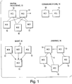
- a number of reconfigurable compute engines 10 may be interconnected so as to perform a number of functions.
- One of the functions may be a spatial processing function illustrated at 12 in which various of the physical layers of the reconfigurable compute engines are interconnected to provide a spatial processing function.
- a communications function 14 is desired, then selected reconfigurable compute engines are connected together for the communications function.
- a signal intelligence function 16 various of the reconfigurable compute engines are interconnected as illustrated, whereas for a jamming function 18 the reconfigurable compute engines may be arranged, for instance, in a ring topography and connected by the subject fabric. As illustrated by dotted line 11, in the ring topography scheme direct connection of RCEs is possible.
- each of the reconfigurable compute engines as illustrated in Figure 2 may include an FPGA 20 with each of the FPGAs having an applications layer 22 an interconnect layer 24 and a physical layer 26 that interconnects the two FPGAs.
- interconnect layer defines the input and output for each of the FPGAs both as to the type of pin that they represent and also which pins are connected to what pins between the FPGAs.
- the applications loaded into the FPGAs may be made to change depending on the mode of operation for the entire system, with the physical layer being a fabric which connects the pins of complementary FPGAs together under the control of the interconnect mechanism which resides in the FPGA interconnect layer.
- each of the RCEs 30, 32, 34 and 36 has a physical layer 40 which constitutes a reconfigurable interconnect mechanism under the control of the interconnect layer within the RCE.
- one interconnect between RCE 30 and RCE 36 supports a strobe 42, whereas for instance, the interconnect 44 between RCE 34 and 36 supports data flow between these two RCEs, with the data flow, for instance, being either circuit switched or packet switched.
- Other types of data can be transmitted between, for instance, RCE 36 and RCE 32 over an interconnection 46 which supports, for instance, discrete signaling in terms of the level of a signal transmitted.
- the subject system is different from the bus structure shown at 50 in which a number of general purpose processors 52 are interconnected by a bus 54 to which are applied time sequenced or multiplex signals such that the interconnection between the general purpose processors is not done in parallel but rather is done serially.
- FIG. 5 what is shown in general is a cross point connection matrix 60 diagrammatically illustrating how complementary FPGAs can be connected by virtue of a fabric.
- a number of transmitter pins 62, 64, 66 and 68 are selectively connected to complementary receiver pins 70, 72, 74 and 76, with the cross point fabric providing the connection of transmitter pin 66 to receiver pin 74 overlying 80 whereas transmitter pin 64 is connected to receiver pin 76 over line 82, with transmitter pin 62 connected to receiver pin 72 over line 84.
- the connections provide a parallel connection as opposed to the serial connection associated with any type of bus structure.
- a number of RCEs 90, 92, 94 and 96 are provided respectively with various functions 98, 100, 102 and 104. These are the functions that are required to be performed by of the RCEs to effectuate a given mode of operation.
- the subject fabric 110 is utilized to interconnect all of the RCEs.
- each of the RCEs is connected to its associated general purpose processor, here respectively illustrated at 112, 114, 116 and 118 interconnected with a second fabric 120 of a conventional Ethernet or other variety.
- Fabric 110 interconnects the RCEs in such a manner as to effectuate the particular mode.
- a number of RCEs 130, 132 and 134 are interconnected by connecting various pins 136, 138, 140 and 142 on RCE 130 to complementary pins 136', 138', 140' and 142'.
- data transmitter pins 136 and 138 on RCE 130 are connected to complementary pins 136' and 138' respectively for RCE 132, which pins correspond to data receiver pins.
- the connections designated by arrows 144 correspond to a connection oriented switched circuit data path between RCE 130 and RCE 132.
- path 146 between strobe transmitter pin 142' at RCE 132 is established by connection to a strobe receiver pin 142 on RCE 130. Note that path 146 represents a connection oriented circuit event strobe path in this case.
- the interconnect layer for each of the RCEs defines the pin and what the function of the pins is so that the physical layer remains invariable, with the pins and their functions being determined by the interconnect layer.
- the physical layer remains unchanged, whereas the interconnect functions are programmable through the programming of the interconnect layer. Note that the programming of the interconnect layer does not affect either the application or the physical layers so that mode changes can be rapidly effectuated utilizing the same or lesser numbers of available RCEs.
Landscapes
- Engineering & Computer Science (AREA)
- Computer Hardware Design (AREA)
- Theoretical Computer Science (AREA)
- Physics & Mathematics (AREA)
- General Engineering & Computer Science (AREA)
- General Physics & Mathematics (AREA)
- Computing Systems (AREA)
- Logic Circuits (AREA)
Claims (9)
- Système employant une pluralité de moteurs de calcul reconfigurables, dans lequel un certain nombre de modes de fonctionnement différents peuvent être effectués selon les interconnexions par lesquelles les moteurs communiquent les uns avec les autres et dans lequel chaque moteur de calcul reconfigurable (20) comprend :une couche physique invariable (26) présentant des broches de connexion destinées à la fourniture d'interconnexion avec une autre de la pluralité de moteurs de calcul reconfigurables ;une couche d'application (22) destinée à la programmation pour réaliser un des dits modes de fonctionnement donnés ;une couche d'interconnexion reconfigurable (24) fournie entre ladite couche d'application (22) et ladite couche physique (26) et apte à être programmée pour indiquer la fonction desdites broches de connexion de façon à accoupler les moteurs ensemble d'une manière à effectuer le mode de fonctionnement donné.
- Système selon la revendication 1, dans lequel les paires desdits moteurs sont complémentaires.
- Système selon la revendication 2, dans lequel lesdites paires de moteurs présentent des broches de connexion complémentaires.
- Système selon la revendication 3, dans lequel lesdites broches de connexion complémentaires peuvent être spécifiées pour présenter respectivement des fonctions de transmission et de réception.
- Système selon la revendication 3, dans lequel lesdites broches de connexion complémentaires peuvent être spécifiées pour présenter la fonction pour transmettre des signaux de synchronisation entre celles-ci.
- Système selon la revendication 5, dans lequel lesdits signaux de synchronisation comprennent une impulsion d'activation.
- Système selon la revendication 3, dans lequel chacune desdites broches de connexion complémentaires prend en charge au moins une parmi la transmission de signaux de commutation par paquets, la transmission de signaux à commutation de circuits et les transmissions de niveau de signal discret.
- Système selon une quelconque revendication précédente, dans lequel au moins un parmi lesdits moteurs de calcul comprend un réseau de portes programmable par l'utilisateur.
- Système selon une quelconque revendication précédente, dans lequel lesdits modes de fonctionnement différents comprennent l'un quelconque parmi : traitement spatial, communications, intelligence de signal ou brouillage.
Applications Claiming Priority (3)
| Application Number | Priority Date | Filing Date | Title |
|---|---|---|---|
| US40681802P | 2002-08-29 | 2002-08-29 | |
| US406818P | 2002-08-29 | ||
| PCT/US2003/020414 WO2004021643A1 (fr) | 2002-08-29 | 2003-06-26 | Matrice d'interconnexion de moteur de calcul reconfigurable |
Publications (3)
| Publication Number | Publication Date |
|---|---|
| EP1530849A1 EP1530849A1 (fr) | 2005-05-18 |
| EP1530849A4 EP1530849A4 (fr) | 2010-06-30 |
| EP1530849B1 true EP1530849B1 (fr) | 2018-10-24 |
Family
ID=31978362
Family Applications (1)
| Application Number | Title | Priority Date | Filing Date |
|---|---|---|---|
| EP03742296.1A Expired - Lifetime EP1530849B1 (fr) | 2002-08-29 | 2003-06-26 | Matrice d'interconnexion de moteur de calcul reconfigurable |
Country Status (4)
| Country | Link |
|---|---|
| US (2) | US7580404B2 (fr) |
| EP (1) | EP1530849B1 (fr) |
| AU (1) | AU2003294080A1 (fr) |
| WO (1) | WO2004021643A1 (fr) |
Families Citing this family (7)
| Publication number | Priority date | Publication date | Assignee | Title |
|---|---|---|---|---|
| US20140051968A1 (en) * | 2007-01-16 | 2014-02-20 | Radiadyne, Llc | Rectal balloon with sensor cable |
| US8151024B2 (en) * | 2009-05-28 | 2012-04-03 | Honeywell International Inc. | Reconfigurable virtual backplane systems and methods |
| US9626624B2 (en) * | 2010-07-20 | 2017-04-18 | Analog Devices, Inc. | Programmable probability processing |
| US8868700B2 (en) * | 2010-12-28 | 2014-10-21 | Nant Holdings Ip, Llc | Distributed network interfaces for application cloaking and spoofing |
| US9563851B2 (en) | 2011-06-07 | 2017-02-07 | Analog Devices, Inc. | Programmable probability processing |
| US12335099B2 (en) | 2020-10-19 | 2025-06-17 | Google Llc | Enhanced reconfigurable interconnect network |
| US11516087B2 (en) * | 2020-11-30 | 2022-11-29 | Google Llc | Connecting processors using twisted torus configurations |
Family Cites Families (25)
| Publication number | Priority date | Publication date | Assignee | Title |
|---|---|---|---|---|
| US5307342A (en) * | 1991-08-30 | 1994-04-26 | International Business Machines Corporation | Heterogeneous ports switch |
| US20020130681A1 (en) * | 1991-09-03 | 2002-09-19 | Cliff Richard G. | Programmable logic array integrated circuits |
| US5802290A (en) * | 1992-07-29 | 1998-09-01 | Virtual Computer Corporation | Computer network of distributed virtual computers which are EAC reconfigurable in response to instruction to be executed |
| US6049223A (en) * | 1995-03-22 | 2000-04-11 | Altera Corporation | Programmable logic array integrated circuit with general-purpose memory configurable as a random access or FIFO memory |
| US5574388A (en) * | 1995-10-13 | 1996-11-12 | Mentor Graphics Corporation | Emulation system having a scalable multi-level multi-stage programmable interconnect network |
| US6421322B1 (en) * | 1997-11-17 | 2002-07-16 | Adc Telecommunications, Inc. | System and method for electronically identifying connections of a cross-connect system |
| FI112301B (fi) * | 1997-12-01 | 2003-11-14 | Nokia Corp | Laajennuskortti |
| US6119171A (en) * | 1998-01-29 | 2000-09-12 | Ip Dynamics, Inc. | Domain name routing |
| US6618392B1 (en) * | 1998-04-17 | 2003-09-09 | Advanced Micro Devices, Inc. | Network transceiver using signal detect input to control modes of operation |
| US6467017B1 (en) * | 1998-06-23 | 2002-10-15 | Altera Corporation | Programmable logic device having embedded dual-port random access memory configurable as single-port memory |
| US6282627B1 (en) * | 1998-06-29 | 2001-08-28 | Chameleon Systems, Inc. | Integrated processor and programmable data path chip for reconfigurable computing |
| US6912223B1 (en) * | 1998-11-03 | 2005-06-28 | Network Technologies Inc. | Automatic router configuration |
| IT1303842B1 (it) * | 1998-11-20 | 2001-03-01 | Cit Alcatel | Rete di telecomunicazione con uno strato di trasporto controllato dauno strato a protocollo internet |
| US6931440B1 (en) * | 1999-04-21 | 2005-08-16 | Emc Corporation | Method and apparatus for dynamically determining whether access to a resource connected to a computer has changed and determining how to access the resource with a new identifier |
| GB0011954D0 (en) * | 2000-05-17 | 2000-07-05 | Univ Surrey | Protocol stacks |
| JP3616559B2 (ja) * | 2000-08-01 | 2005-02-02 | 日本電気通信システム株式会社 | 通信装置 |
| US20020161923A1 (en) * | 2001-04-27 | 2002-10-31 | Foster Michael S. | Method and system for reconfiguring a path in a communications network |
| US6721312B2 (en) * | 2001-06-01 | 2004-04-13 | Pluris, Inc. | Method and apparatus for improving data transmission in router fabric cards through pseudo-synchronous data switching |
| CN1593050A (zh) * | 2001-09-26 | 2005-03-09 | 皇家飞利浦电子股份有限公司 | 用于可重新配置多媒体系统的方法和装置 |
| US7126214B2 (en) * | 2001-12-05 | 2006-10-24 | Arbor Company Llp | Reconfigurable processor module comprising hybrid stacked integrated circuit die elements |
| WO2003053084A1 (fr) * | 2001-12-14 | 2003-06-26 | California Institute Of Technology | Protocoles reconfigurables et architectures pour reseaux sans fil |
| US6996443B2 (en) * | 2002-01-11 | 2006-02-07 | Bae Systems Information And Electronic Systems Integration Inc. | Reconfigurable digital processing system for space |
| US7080156B2 (en) * | 2002-03-21 | 2006-07-18 | Sun Microsystems, Inc. | Message routing in a torus interconnect |
| US7093225B2 (en) * | 2002-07-17 | 2006-08-15 | Osann Robert Jr | FPGA with hybrid interconnect |
| US7269168B2 (en) * | 2002-07-31 | 2007-09-11 | Brocade Communications Systems, Inc. | Host bus adaptor-based virtualization switch |
-
2003
- 2003-06-26 WO PCT/US2003/020414 patent/WO2004021643A1/fr not_active Ceased
- 2003-06-26 US US10/530,160 patent/US7580404B2/en not_active Expired - Lifetime
- 2003-06-26 EP EP03742296.1A patent/EP1530849B1/fr not_active Expired - Lifetime
- 2003-06-26 AU AU2003294080A patent/AU2003294080A1/en not_active Abandoned
-
2009
- 2009-08-24 US US12/546,657 patent/US8411676B2/en not_active Expired - Fee Related
Non-Patent Citations (1)
| Title |
|---|
| None * |
Also Published As
| Publication number | Publication date |
|---|---|
| WO2004021643A1 (fr) | 2004-03-11 |
| EP1530849A4 (fr) | 2010-06-30 |
| US20100014513A1 (en) | 2010-01-21 |
| US7580404B2 (en) | 2009-08-25 |
| EP1530849A1 (fr) | 2005-05-18 |
| US8411676B2 (en) | 2013-04-02 |
| US20060109842A1 (en) | 2006-05-25 |
| AU2003294080A1 (en) | 2004-03-19 |
Similar Documents
| Publication | Publication Date | Title |
|---|---|---|
| US8411676B2 (en) | Reconfigurable compute engine interconnect fabric | |
| Dielissen et al. | Concepts and implementation of the Philips network-on-chip | |
| US6049542A (en) | Scalable multistage interconnection network architecture and method for performing in-service upgrade thereof | |
| US4032893A (en) | Reconfigurable data bus | |
| US6181159B1 (en) | Integrated circuit incorporating a programmable cross-bar switch | |
| US6611518B1 (en) | Methods and apparatus for flexible device interface port assignment in a data communications switching system | |
| Gwaltney et al. | Comparison of communication architectures for spacecraft modular avionics systems | |
| US5875314A (en) | Configurable connection fabric for providing serial backplanes with adaptive port/module bandwidth | |
| CN109690515A (zh) | 用于在基于管线的网络拓扑中执行部分重新配置的方法和设备 | |
| JPH05241947A (ja) | 分散クロスバー・スイッチ・アーキテクチャにおける交換接続の配列。 | |
| JPH11136271A (ja) | 複数セグメント中継器 | |
| EP1249971A2 (fr) | Interface de réseau utilisant un retard programmable et un doubleur de fréquence | |
| US20040054818A1 (en) | Flexible results pipeline for processing element | |
| US6333641B1 (en) | Apparatus and methods for dynamically defining variably sized autonomous sub-arrays within a programmable gate array | |
| Adetomi et al. | Relocation-aware communication network for circuits on Xilinx FPGAs | |
| Parkes et al. | A prototype SpaceVPX lite (vita 78.1) system using SpaceFibre for data and control planes | |
| US7114017B2 (en) | Programmable peripheral switch | |
| CN223598232U (zh) | 处理器互联结构、主板及服务器 | |
| Hironaka et al. | Demonstration of flow-in-cloud: A multi-fpga system | |
| Montenegro et al. | Network centric systems for space applications | |
| US20260005985A1 (en) | Structured reconfigurable wiring functions through routers in network-on-chip | |
| RU2177674C2 (ru) | Система передачи информации | |
| Kosyanchuk et al. | Analysis of the requirements to information exchange protocol for an all-optical onboard network | |
| GB2582708A (en) | A networked computer | |
| US20210303315A1 (en) | Application logic architecture defining separate processing planes |
Legal Events
| Date | Code | Title | Description |
|---|---|---|---|
| PUAI | Public reference made under article 153(3) epc to a published international application that has entered the european phase |
Free format text: ORIGINAL CODE: 0009012 |
|
| 17P | Request for examination filed |
Effective date: 20050221 |
|
| AK | Designated contracting states |
Kind code of ref document: A1 Designated state(s): AT BE BG CH CY CZ DE DK EE ES FI FR GB GR HU IE IT LI LU MC NL PT RO SE SI SK TR |
|
| AX | Request for extension of the european patent |
Extension state: AL LT LV MK |
|
| DAX | Request for extension of the european patent (deleted) | ||
| RAP1 | Party data changed (applicant data changed or rights of an application transferred) |
Owner name: WISTERIUM DEVELOPMENT LLC |
|
| A4 | Supplementary search report drawn up and despatched |
Effective date: 20100531 |
|
| 17Q | First examination report despatched |
Effective date: 20110530 |
|
| STAA | Information on the status of an ep patent application or granted ep patent |
Free format text: STATUS: EXAMINATION IS IN PROGRESS |
|
| RAP1 | Party data changed (applicant data changed or rights of an application transferred) |
Owner name: CALLAHAN CELLULAR L.L.C. |
|
| GRAP | Despatch of communication of intention to grant a patent |
Free format text: ORIGINAL CODE: EPIDOSNIGR1 |
|
| STAA | Information on the status of an ep patent application or granted ep patent |
Free format text: STATUS: GRANT OF PATENT IS INTENDED |
|
| INTG | Intention to grant announced |
Effective date: 20180523 |
|
| GRAS | Grant fee paid |
Free format text: ORIGINAL CODE: EPIDOSNIGR3 |
|
| GRAA | (expected) grant |
Free format text: ORIGINAL CODE: 0009210 |
|
| STAA | Information on the status of an ep patent application or granted ep patent |
Free format text: STATUS: THE PATENT HAS BEEN GRANTED |
|
| AK | Designated contracting states |
Kind code of ref document: B1 Designated state(s): AT BE BG CH CY CZ DE DK EE ES FI FR GB GR HU IE IT LI LU MC NL PT RO SE SI SK TR |
|
| REG | Reference to a national code |
Ref country code: GB Ref legal event code: FG4D |
|
| REG | Reference to a national code |
Ref country code: CH Ref legal event code: EP |
|
| REG | Reference to a national code |
Ref country code: IE Ref legal event code: FG4D |
|
| REG | Reference to a national code |
Ref country code: AT Ref legal event code: REF Ref document number: 1057983 Country of ref document: AT Kind code of ref document: T Effective date: 20181115 |
|
| REG | Reference to a national code |
Ref country code: DE Ref legal event code: R096 Ref document number: 60351580 Country of ref document: DE |
|
| REG | Reference to a national code |
Ref country code: CH Ref legal event code: PK Free format text: BERICHTIGUNGEN |
|
| RIC2 | Information provided on ipc code assigned after grant |
Ipc: H04J 3/16 20060101ALI20040316BHEP Ipc: H04L 12/28 20060101AFI20040316BHEP |
|
| REG | Reference to a national code |
Ref country code: NL Ref legal event code: MP Effective date: 20181024 |
|
| REG | Reference to a national code |
Ref country code: AT Ref legal event code: MK05 Ref document number: 1057983 Country of ref document: AT Kind code of ref document: T Effective date: 20181024 |
|
| PG25 | Lapsed in a contracting state [announced via postgrant information from national office to epo] |
Ref country code: NL Free format text: LAPSE BECAUSE OF FAILURE TO SUBMIT A TRANSLATION OF THE DESCRIPTION OR TO PAY THE FEE WITHIN THE PRESCRIBED TIME-LIMIT Effective date: 20181024 |
|
| PG25 | Lapsed in a contracting state [announced via postgrant information from national office to epo] |
Ref country code: FI Free format text: LAPSE BECAUSE OF FAILURE TO SUBMIT A TRANSLATION OF THE DESCRIPTION OR TO PAY THE FEE WITHIN THE PRESCRIBED TIME-LIMIT Effective date: 20181024 Ref country code: AT Free format text: LAPSE BECAUSE OF FAILURE TO SUBMIT A TRANSLATION OF THE DESCRIPTION OR TO PAY THE FEE WITHIN THE PRESCRIBED TIME-LIMIT Effective date: 20181024 Ref country code: ES Free format text: LAPSE BECAUSE OF FAILURE TO SUBMIT A TRANSLATION OF THE DESCRIPTION OR TO PAY THE FEE WITHIN THE PRESCRIBED TIME-LIMIT Effective date: 20181024 Ref country code: BG Free format text: LAPSE BECAUSE OF FAILURE TO SUBMIT A TRANSLATION OF THE DESCRIPTION OR TO PAY THE FEE WITHIN THE PRESCRIBED TIME-LIMIT Effective date: 20190124 |
|
| PG25 | Lapsed in a contracting state [announced via postgrant information from national office to epo] |
Ref country code: PT Free format text: LAPSE BECAUSE OF FAILURE TO SUBMIT A TRANSLATION OF THE DESCRIPTION OR TO PAY THE FEE WITHIN THE PRESCRIBED TIME-LIMIT Effective date: 20190224 Ref country code: SE Free format text: LAPSE BECAUSE OF FAILURE TO SUBMIT A TRANSLATION OF THE DESCRIPTION OR TO PAY THE FEE WITHIN THE PRESCRIBED TIME-LIMIT Effective date: 20181024 Ref country code: GR Free format text: LAPSE BECAUSE OF FAILURE TO SUBMIT A TRANSLATION OF THE DESCRIPTION OR TO PAY THE FEE WITHIN THE PRESCRIBED TIME-LIMIT Effective date: 20190125 |
|
| REG | Reference to a national code |
Ref country code: DE Ref legal event code: R097 Ref document number: 60351580 Country of ref document: DE |
|
| PG25 | Lapsed in a contracting state [announced via postgrant information from national office to epo] |
Ref country code: CZ Free format text: LAPSE BECAUSE OF FAILURE TO SUBMIT A TRANSLATION OF THE DESCRIPTION OR TO PAY THE FEE WITHIN THE PRESCRIBED TIME-LIMIT Effective date: 20181024 Ref country code: IT Free format text: LAPSE BECAUSE OF FAILURE TO SUBMIT A TRANSLATION OF THE DESCRIPTION OR TO PAY THE FEE WITHIN THE PRESCRIBED TIME-LIMIT Effective date: 20181024 Ref country code: DK Free format text: LAPSE BECAUSE OF FAILURE TO SUBMIT A TRANSLATION OF THE DESCRIPTION OR TO PAY THE FEE WITHIN THE PRESCRIBED TIME-LIMIT Effective date: 20181024 |
|
| PG25 | Lapsed in a contracting state [announced via postgrant information from national office to epo] |
Ref country code: EE Free format text: LAPSE BECAUSE OF FAILURE TO SUBMIT A TRANSLATION OF THE DESCRIPTION OR TO PAY THE FEE WITHIN THE PRESCRIBED TIME-LIMIT Effective date: 20181024 Ref country code: SK Free format text: LAPSE BECAUSE OF FAILURE TO SUBMIT A TRANSLATION OF THE DESCRIPTION OR TO PAY THE FEE WITHIN THE PRESCRIBED TIME-LIMIT Effective date: 20181024 Ref country code: RO Free format text: LAPSE BECAUSE OF FAILURE TO SUBMIT A TRANSLATION OF THE DESCRIPTION OR TO PAY THE FEE WITHIN THE PRESCRIBED TIME-LIMIT Effective date: 20181024 |
|
| PLBE | No opposition filed within time limit |
Free format text: ORIGINAL CODE: 0009261 |
|
| STAA | Information on the status of an ep patent application or granted ep patent |
Free format text: STATUS: NO OPPOSITION FILED WITHIN TIME LIMIT |
|
| 26N | No opposition filed |
Effective date: 20190725 |
|
| PG25 | Lapsed in a contracting state [announced via postgrant information from national office to epo] |
Ref country code: SI Free format text: LAPSE BECAUSE OF FAILURE TO SUBMIT A TRANSLATION OF THE DESCRIPTION OR TO PAY THE FEE WITHIN THE PRESCRIBED TIME-LIMIT Effective date: 20181024 |
|
| PG25 | Lapsed in a contracting state [announced via postgrant information from national office to epo] |
Ref country code: MC Free format text: LAPSE BECAUSE OF FAILURE TO SUBMIT A TRANSLATION OF THE DESCRIPTION OR TO PAY THE FEE WITHIN THE PRESCRIBED TIME-LIMIT Effective date: 20181024 |
|
| REG | Reference to a national code |
Ref country code: CH Ref legal event code: PL |
|
| REG | Reference to a national code |
Ref country code: BE Ref legal event code: MM Effective date: 20190630 |
|
| PG25 | Lapsed in a contracting state [announced via postgrant information from national office to epo] |
Ref country code: TR Free format text: LAPSE BECAUSE OF FAILURE TO SUBMIT A TRANSLATION OF THE DESCRIPTION OR TO PAY THE FEE WITHIN THE PRESCRIBED TIME-LIMIT Effective date: 20181024 |
|
| PG25 | Lapsed in a contracting state [announced via postgrant information from national office to epo] |
Ref country code: IE Free format text: LAPSE BECAUSE OF NON-PAYMENT OF DUE FEES Effective date: 20190626 |
|
| PG25 | Lapsed in a contracting state [announced via postgrant information from national office to epo] |
Ref country code: LU Free format text: LAPSE BECAUSE OF NON-PAYMENT OF DUE FEES Effective date: 20190626 Ref country code: BE Free format text: LAPSE BECAUSE OF NON-PAYMENT OF DUE FEES Effective date: 20190630 Ref country code: CH Free format text: LAPSE BECAUSE OF NON-PAYMENT OF DUE FEES Effective date: 20190630 Ref country code: LI Free format text: LAPSE BECAUSE OF NON-PAYMENT OF DUE FEES Effective date: 20190630 |
|
| PG25 | Lapsed in a contracting state [announced via postgrant information from national office to epo] |
Ref country code: CY Free format text: LAPSE BECAUSE OF FAILURE TO SUBMIT A TRANSLATION OF THE DESCRIPTION OR TO PAY THE FEE WITHIN THE PRESCRIBED TIME-LIMIT Effective date: 20181024 |
|
| PG25 | Lapsed in a contracting state [announced via postgrant information from national office to epo] |
Ref country code: HU Free format text: LAPSE BECAUSE OF FAILURE TO SUBMIT A TRANSLATION OF THE DESCRIPTION OR TO PAY THE FEE WITHIN THE PRESCRIBED TIME-LIMIT; INVALID AB INITIO Effective date: 20030626 |
|
| PGFP | Annual fee paid to national office [announced via postgrant information from national office to epo] |
Ref country code: GB Payment date: 20220526 Year of fee payment: 20 Ref country code: FR Payment date: 20220517 Year of fee payment: 20 Ref country code: DE Payment date: 20220512 Year of fee payment: 20 |
|
| REG | Reference to a national code |
Ref country code: DE Ref legal event code: R071 Ref document number: 60351580 Country of ref document: DE |
|
| P01 | Opt-out of the competence of the unified patent court (upc) registered |
Effective date: 20230522 |
|
| REG | Reference to a national code |
Ref country code: GB Ref legal event code: PE20 Expiry date: 20230625 |
|
| PG25 | Lapsed in a contracting state [announced via postgrant information from national office to epo] |
Ref country code: GB Free format text: LAPSE BECAUSE OF EXPIRATION OF PROTECTION Effective date: 20230625 |