EP1533876B1 - Contrôle de polarisation dans une diode laser verticale utilisant un réseau monolithiquement intégré - Google Patents
Contrôle de polarisation dans une diode laser verticale utilisant un réseau monolithiquement intégré Download PDFInfo
- Publication number
- EP1533876B1 EP1533876B1 EP04026958.1A EP04026958A EP1533876B1 EP 1533876 B1 EP1533876 B1 EP 1533876B1 EP 04026958 A EP04026958 A EP 04026958A EP 1533876 B1 EP1533876 B1 EP 1533876B1
- Authority
- EP
- European Patent Office
- Prior art keywords
- bragg reflector
- layer
- layer sequence
- laser
- reflector layer
- Prior art date
- Legal status (The legal status is an assumption and is not a legal conclusion. Google has not performed a legal analysis and makes no representation as to the accuracy of the status listed.)
- Expired - Lifetime
Links
- 230000010287 polarization Effects 0.000 claims description 33
- 230000000737 periodic effect Effects 0.000 claims description 30
- 238000000034 method Methods 0.000 claims description 22
- 230000008569 process Effects 0.000 claims description 16
- 238000005530 etching Methods 0.000 claims description 15
- 239000000758 substrate Substances 0.000 claims description 14
- 239000000463 material Substances 0.000 claims description 7
- 230000003287 optical effect Effects 0.000 claims description 7
- 229910052751 metal Inorganic materials 0.000 claims description 5
- 239000002184 metal Substances 0.000 claims description 5
- 230000005855 radiation Effects 0.000 claims description 5
- 230000005540 biological transmission Effects 0.000 claims description 4
- 239000003989 dielectric material Substances 0.000 claims description 4
- 239000000126 substance Substances 0.000 claims description 4
- 238000010521 absorption reaction Methods 0.000 claims description 3
- 238000004519 manufacturing process Methods 0.000 claims description 2
- 238000000151 deposition Methods 0.000 claims 3
- 239000013078 crystal Substances 0.000 description 4
- 238000000059 patterning Methods 0.000 description 4
- 230000008859 change Effects 0.000 description 3
- 229910001218 Gallium arsenide Inorganic materials 0.000 description 2
- 230000001419 dependent effect Effects 0.000 description 2
- 230000000694 effects Effects 0.000 description 2
- 238000005516 engineering process Methods 0.000 description 2
- 238000007639 printing Methods 0.000 description 2
- 230000001629 suppression Effects 0.000 description 2
- 229910000980 Aluminium gallium arsenide Inorganic materials 0.000 description 1
- RTAQQCXQSZGOHL-UHFFFAOYSA-N Titanium Chemical compound [Ti] RTAQQCXQSZGOHL-UHFFFAOYSA-N 0.000 description 1
- 229910052782 aluminium Inorganic materials 0.000 description 1
- XAGFODPZIPBFFR-UHFFFAOYSA-N aluminium Chemical compound [Al] XAGFODPZIPBFFR-UHFFFAOYSA-N 0.000 description 1
- 238000013459 approach Methods 0.000 description 1
- 238000004891 communication Methods 0.000 description 1
- 238000001816 cooling Methods 0.000 description 1
- 230000008878 coupling Effects 0.000 description 1
- 238000010168 coupling process Methods 0.000 description 1
- 238000005859 coupling reaction Methods 0.000 description 1
- 230000006866 deterioration Effects 0.000 description 1
- 238000011161 development Methods 0.000 description 1
- 230000018109 developmental process Effects 0.000 description 1
- 238000009429 electrical wiring Methods 0.000 description 1
- 238000005265 energy consumption Methods 0.000 description 1
- 230000006355 external stress Effects 0.000 description 1
- 239000000835 fiber Substances 0.000 description 1
- PCHJSUWPFVWCPO-UHFFFAOYSA-N gold Chemical compound [Au] PCHJSUWPFVWCPO-UHFFFAOYSA-N 0.000 description 1
- 229910052737 gold Inorganic materials 0.000 description 1
- 239000010931 gold Substances 0.000 description 1
- 238000009434 installation Methods 0.000 description 1
- 238000009413 insulation Methods 0.000 description 1
- 239000011159 matrix material Substances 0.000 description 1
- 150000002739 metals Chemical class 0.000 description 1
- 239000013307 optical fiber Substances 0.000 description 1
- 230000005693 optoelectronics Effects 0.000 description 1
- 238000004611 spectroscopical analysis Methods 0.000 description 1
- 238000012360 testing method Methods 0.000 description 1
- 239000010936 titanium Substances 0.000 description 1
- 229910052719 titanium Inorganic materials 0.000 description 1
- 230000007704 transition Effects 0.000 description 1
- 238000003631 wet chemical etching Methods 0.000 description 1
Images

Classifications
-
- H—ELECTRICITY
- H01—ELECTRIC ELEMENTS
- H01S—DEVICES USING THE PROCESS OF LIGHT AMPLIFICATION BY STIMULATED EMISSION OF RADIATION [LASER] TO AMPLIFY OR GENERATE LIGHT; DEVICES USING STIMULATED EMISSION OF ELECTROMAGNETIC RADIATION IN WAVE RANGES OTHER THAN OPTICAL
- H01S5/00—Semiconductor lasers
- H01S5/10—Construction or shape of the optical resonator, e.g. extended or external cavity, coupled cavities, bent-guide, varying width, thickness or composition of the active region
- H01S5/18—Surface-emitting [SE] lasers, e.g. having both horizontal and vertical cavities
- H01S5/183—Surface-emitting [SE] lasers, e.g. having both horizontal and vertical cavities having only vertical cavities, e.g. vertical cavity surface-emitting lasers [VCSEL]
- H01S5/18355—Surface-emitting [SE] lasers, e.g. having both horizontal and vertical cavities having only vertical cavities, e.g. vertical cavity surface-emitting lasers [VCSEL] having a defined polarisation
-
- H—ELECTRICITY
- H01—ELECTRIC ELEMENTS
- H01S—DEVICES USING THE PROCESS OF LIGHT AMPLIFICATION BY STIMULATED EMISSION OF RADIATION [LASER] TO AMPLIFY OR GENERATE LIGHT; DEVICES USING STIMULATED EMISSION OF ELECTROMAGNETIC RADIATION IN WAVE RANGES OTHER THAN OPTICAL
- H01S2301/00—Functional characteristics
- H01S2301/16—Semiconductor lasers with special structural design to influence the modes, e.g. specific multimode
- H01S2301/166—Single transverse or lateral mode
-
- H—ELECTRICITY
- H01—ELECTRIC ELEMENTS
- H01S—DEVICES USING THE PROCESS OF LIGHT AMPLIFICATION BY STIMULATED EMISSION OF RADIATION [LASER] TO AMPLIFY OR GENERATE LIGHT; DEVICES USING STIMULATED EMISSION OF ELECTROMAGNETIC RADIATION IN WAVE RANGES OTHER THAN OPTICAL
- H01S5/00—Semiconductor lasers
- H01S5/10—Construction or shape of the optical resonator, e.g. extended or external cavity, coupled cavities, bent-guide, varying width, thickness or composition of the active region
- H01S5/18—Surface-emitting [SE] lasers, e.g. having both horizontal and vertical cavities
- H01S5/183—Surface-emitting [SE] lasers, e.g. having both horizontal and vertical cavities having only vertical cavities, e.g. vertical cavity surface-emitting lasers [VCSEL]
- H01S5/18308—Surface-emitting [SE] lasers, e.g. having both horizontal and vertical cavities having only vertical cavities, e.g. vertical cavity surface-emitting lasers [VCSEL] having a special structure for lateral current or light confinement
- H01S5/18311—Surface-emitting [SE] lasers, e.g. having both horizontal and vertical cavities having only vertical cavities, e.g. vertical cavity surface-emitting lasers [VCSEL] having a special structure for lateral current or light confinement using selective oxidation
- H01S5/18313—Surface-emitting [SE] lasers, e.g. having both horizontal and vertical cavities having only vertical cavities, e.g. vertical cavity surface-emitting lasers [VCSEL] having a special structure for lateral current or light confinement using selective oxidation by oxidizing at least one of the DBR layers
-
- H—ELECTRICITY
- H01—ELECTRIC ELEMENTS
- H01S—DEVICES USING THE PROCESS OF LIGHT AMPLIFICATION BY STIMULATED EMISSION OF RADIATION [LASER] TO AMPLIFY OR GENERATE LIGHT; DEVICES USING STIMULATED EMISSION OF ELECTROMAGNETIC RADIATION IN WAVE RANGES OTHER THAN OPTICAL
- H01S5/00—Semiconductor lasers
- H01S5/10—Construction or shape of the optical resonator, e.g. extended or external cavity, coupled cavities, bent-guide, varying width, thickness or composition of the active region
- H01S5/18—Surface-emitting [SE] lasers, e.g. having both horizontal and vertical cavities
- H01S5/183—Surface-emitting [SE] lasers, e.g. having both horizontal and vertical cavities having only vertical cavities, e.g. vertical cavity surface-emitting lasers [VCSEL]
- H01S5/18308—Surface-emitting [SE] lasers, e.g. having both horizontal and vertical cavities having only vertical cavities, e.g. vertical cavity surface-emitting lasers [VCSEL] having a special structure for lateral current or light confinement
- H01S5/18319—Surface-emitting [SE] lasers, e.g. having both horizontal and vertical cavities having only vertical cavities, e.g. vertical cavity surface-emitting lasers [VCSEL] having a special structure for lateral current or light confinement comprising a periodical structure in lateral directions
-
- H—ELECTRICITY
- H01—ELECTRIC ELEMENTS
- H01S—DEVICES USING THE PROCESS OF LIGHT AMPLIFICATION BY STIMULATED EMISSION OF RADIATION [LASER] TO AMPLIFY OR GENERATE LIGHT; DEVICES USING STIMULATED EMISSION OF ELECTROMAGNETIC RADIATION IN WAVE RANGES OTHER THAN OPTICAL
- H01S5/00—Semiconductor lasers
- H01S5/10—Construction or shape of the optical resonator, e.g. extended or external cavity, coupled cavities, bent-guide, varying width, thickness or composition of the active region
- H01S5/18—Surface-emitting [SE] lasers, e.g. having both horizontal and vertical cavities
- H01S5/183—Surface-emitting [SE] lasers, e.g. having both horizontal and vertical cavities having only vertical cavities, e.g. vertical cavity surface-emitting lasers [VCSEL]
- H01S5/18344—Surface-emitting [SE] lasers, e.g. having both horizontal and vertical cavities having only vertical cavities, e.g. vertical cavity surface-emitting lasers [VCSEL] characterized by the mesa, e.g. dimensions or shape of the mesa
- H01S5/18347—Mesa comprising active layer
-
- H—ELECTRICITY
- H01—ELECTRIC ELEMENTS
- H01S—DEVICES USING THE PROCESS OF LIGHT AMPLIFICATION BY STIMULATED EMISSION OF RADIATION [LASER] TO AMPLIFY OR GENERATE LIGHT; DEVICES USING STIMULATED EMISSION OF ELECTROMAGNETIC RADIATION IN WAVE RANGES OTHER THAN OPTICAL
- H01S5/00—Semiconductor lasers
- H01S5/10—Construction or shape of the optical resonator, e.g. extended or external cavity, coupled cavities, bent-guide, varying width, thickness or composition of the active region
- H01S5/18—Surface-emitting [SE] lasers, e.g. having both horizontal and vertical cavities
- H01S5/183—Surface-emitting [SE] lasers, e.g. having both horizontal and vertical cavities having only vertical cavities, e.g. vertical cavity surface-emitting lasers [VCSEL]
- H01S5/18386—Details of the emission surface for influencing the near- or far-field, e.g. a grating on the surface
Definitions
- the invention relates generally to vertical diode lasers, and more particularly to vertical diode lasers having at least one patterned layer, and to their manufacture and use.
- Diode lasers occupy an outstanding position in laser technology since the mid-eighties. High efficiency, compactness and easy handling are the main advantages of the diode laser. So far, they have been used above all in communications and information technology, in fiber optic networks and CD players, right up to laser printers and professional printing systems.
- the Vertical Diode Laser (Vertical Cavity Surface Emitting Lasers VCSEL) has proven that compared to the so-called edge emitters, which emit the laser light parallel to the substrate, ie laterally, mainly by easier installation and cooling and better optical properties of the laser light , Further advantages are lower energy consumption and a more compact electrical wiring, which offers price advantages, especially for high-volume applications, as well as the option for on-wafer testing.
- VCSEL Vertical Diode Laser
- conventional vertical diode lasers do not have a defined direction of polarization. While with edge emitters the light propagation is parallel to the quantum film and thus the transition matrix elements differ for the two polarization directions, the propagation wave vector at VCSELn is perpendicular to the quantum films, whereby the gain is the same for all conceivable polarizations.
- the cylindrical resonator of conventional VCSEL also does not favor polarization.
- the linear electro-optic effect causes a deformation of the refractive index ellipsoid along the crystal axes [011] and [0-11] in VCSELs with the result that the polarization of the fundamental mode of a vertical laser diode is mostly aligned along one of these two crystal axes.
- the next higher mode is generally polarized orthogonal to the fundamental mode.
- a current change or an additional external stress can cause an abrupt change in the polarization of a mode between the two crystal axes.
- the polarization jumps are disadvantageous in printing systems in which media are printed, which have a different absorption for different polarizations.
- the polarization jumps in the optical data transmission lead to increased noise.
- the polarization jumps can prevent the use in spectroscopy by the influence on the emission wavelength.
- a VCSEL with a Guided Mode Grating Resonance Reflector Filter is known.
- GMGRF Guided Mode Grating Resonance Reflector Filter
- the grid of the GMGRF can be integrated into the upper mirror of the VCSEL.
- a VCSEL is known in which there is a structuring which generates a photonic bandgap. This structure prevents the passage of the laser light. In the structuring, an aperture is provided through which the laser light passes. Due to the photonic band gap and the aperture unwanted modes are to be suppressed.
- the invention has for its object to provide a way how the polarization direction of single- and multi-mode vertical diode lasers for all modes and all operating conditions can be set arbitrarily relative to the crystal structure in a particular direction.
- a vertical diode laser comprises at least one substrate, a first Bragg reflector layer sequence applied to the substrate, an applied on the first Bragg reflector layer sequence active layer sequence for generating laser radiation, applied to the active layer sequence second Bragg reflector layer sequence and means for applying a voltage across the active layer sequence, wherein at least the uppermost layer of the second Bragg reflector Layer sequence is periodically structured and wherein the period of structuring and the position of structuring in the beam direction of the laser is selected such that the polarization of the laser is stabilized, the uppermost layer of the second Bragg reflector layer sequence has a recess in the form of a circular center of the ring Has light exit surface of the laser, so that the fundamental mode of the laser is preferably amplified and the structuring is arranged on a circular elevation centrally to the light exit surface of the laser.
- the periodic structuring is formed as a grid.
- the Bragg reflector layer sequences are composed of a plurality of layer pairs, each pair each comprising a high-refractive and a low-refractive layer.
- the layers have a thickness corresponding to the optical path length of 1/4, with 1 the emission wavelength of the VCSEL.
- the layer pairs may comprise AlGaAs, each with a different concentration of aluminum.
- the substrate could, for example, comprise GaAs. However, any other suitable materials can also be used.
- the active layer sequence has at least one, usually multiple quantum wells (Multiple Quantum Wells; MQW).
- the Bragg reflector layer sequences may have one or more further layers to the described 1/4 layers, which may preferably be formed as the uppermost layer or layers.
- One of these further layers may also have periodic structuring.
- the inventors have found that by means of a periodic structuring, by means of a grating, the polarization of a VCSEL can be stabilized and, moreover, also be aligned in a defined manner. This also applies to multi-mode VCSELs. For example, it has been shown experimentally by the inventors that even with highly multi-mode vertical diode lasers having up to 14 modes, suppression of the orthogonal polarization of 15 dB over the entire characteristic at an output power of up to 8 mW can be achieved by a surface grating according to the invention , Polarization jumps with a change in current or temperature or with the addition of an external bias were not observed over the entire characteristic.
- the inventors have surprisingly found that it is imperative for the polarization control of a VCSEL, position, depth and period of the periodic Structuring to select very precisely. Period and depth are strongly dependent on the layer structure.
- the periodic structuring has a period between 0.3 and 1.5 mm, in particular between 0.6 and 1.0 mm.
- the periodic patterning preferably has a value between 0.5 1 and 1.5 1, in particular between 0.7 1 and 1.3 1, on.
- the periodic patterning is also preferably formed as a surface structure of the uppermost layer of the second Bragg reflector layer sequence.
- the structuring can be formed by recesses in this layer.
- the position of the recesses is in addition to the period and the depth of the structuring of the parameters, which significantly influences the polarization properties of the VCSEL according to the invention.
- the recesses have a depth between 10 and 150 nm, in particular between 40 and 90 nm.
- the depth of the recesses at a period of patterning of 0.7 mm preferably has values between 40-70 nm.
- the periodic structuring may also be carried out on the uppermost layer of the second Bragg reflector layer sequence by applying a structure comprising at least one metal or a dielectric material.
- At least one further layer can also be applied and structured. Also, applying further layers above and below the structured layer having different thicknesses is within the scope of the invention.
- the periodic structuring can also be formed by elevations applied to the uppermost layer of the second Bragg reflector layer sequence.
- the uppermost 1/4-layer of the second Bragg reflector layer sequence can first be thinned out. This can be done by applying the top layer with a thickness less than 1/4 or by subsequent full-area etching of this layer.
- the surface relief can be formed in principle in two ways.
- the uppermost layer of the second Bragg reflector layer sequence may have a recess or it may be applied to the uppermost layer of the second Bragg reflector layer sequence another layer with a suitable structuring.
- the top layer of the second Bragg reflector layer sequence has a recess in the form of a circular ring of different thickness centrally to the light exit surface of the laser, whereby only one area in the middle of the light exit surface with a thickness of substantially 1/4 remains.
- a method for producing a polarization-stable VCSEL comprises the provision of a substrate, the application of a first Bragg reflector layer sequence to the substrate, the application of an active layer sequence to the first Bragg reflector layer sequence for generating laser radiation, the application of a second Bragg Reflector layer sequence on the active layer sequence, as well as providing a means for applying a voltage across the active layer sequence, wherein at least the uppermost layer of the second Bragg reflector layer sequence is applied periodically structured and wherein the period, the depth and the position of Structuring in the beam direction of the laser is selected such that the polarization of the laser is stabilized characterized by the step of etching a recess having a cross section in the form of a circular ring in the uppermost layer of the second Bragg reflector layer sequence, so that a circular Shaped elevation is formed centrally to the light exit surface of the laser, so that the power of the fundamental mode of the laser is preferably amplified and the structuring on the circular elevation is arranged centrally to the
- the application of the at least one layer with a periodic structuring comprises the application of a layer which has a lattice structure.
- the period, depth and position of the structuring in the beam direction, which are preferably to be observed in the method according to the invention for producing a polarization-stable VCSEL, correspond to those described above for the VCSEL.
- the uppermost layer of the second Bragg reflector layer sequence is applied in a periodically structured manner, wherein in particular the surface of the layer is patterned.
- the structuring can be carried out by means of conventional photolithographic methods, wherein trenches are etched into the surface of the layer by means of dry-chemical and / or wet-chemical and / or physical etching processes.
- the etching depth is preferably between 10 and 150 nm, in particular between 40 and 90 nm.
- An alternative variant of the application of the at least one layer with a periodic structuring provides for thinning out the uppermost layer of the second Bragg reflector layer sequence initially with respect to the thickness of usually 1/4. This This can be done by already applying the layer with a smaller thickness or by subsequent etching.
- the layer thickness, by which the uppermost layer of the second Bragg reflector layer sequence is thinned is preferably between 10 and 150 nm, in particular between 40 and 90 nm.
- a dielectric material or a metal can be used.
- several materials can be sequentially deposited, such as the metals titanium and gold.
- the method according to the invention provides for applying at least one layer of the layer sequences with a further structuring such that the power of at least one laser mode is preferably amplified.
- the method provides for etching a recess with a cross section in the form of a circular ring in the uppermost layer of the second Bragg reflector layer sequence, so that a projection is formed centrally to the light exit surface of the laser.
- the invention comprises a spectroscopic system, in particular for measuring absorption lines, which has a vertical diode laser according to the invention.
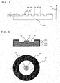
- Fig. 1 schematically shows the structure of a VCSEL 1.
- a first Bragg reflector layer sequence 21 is applied on a substrate 10, for example, a GaAs substrate.
- an active layer sequence 30 is arranged, which has a plurality of quantum wells and serves to generate the laser radiation.
- an oxide aperture 40 is provided within the second Bragg reflector layer sequence 22, which has metallic contact surfaces 61 and 62, as well as an insulation 50. Alternatively, the VCSEL could, for example, also have an intra-cavity contact.
- the uppermost layer of the second Bragg reflector layer sequence 22 has a surface grating 80 with trenches etched into the layer and parallel to one another.
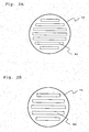
- FIGS. 2A and 2B Various lattice structures studied for VCSELs with emission wavelengths of 850 nm and 960 nm are in the FIGS. 2A and 2B shown in supervision. Shown are in each case the boundary of the contact ring 70, as well as in the uppermost layer of the second Bragg reflector layer sequence etched lattice trenches 81 and 82nd
- Periodic structuring shown have a lattice trench in the middle.
- the structuring could also be shifted in the layer plane for this purpose.
- the periodic structuring could also have a central elevation.
- the grating period is 0.7 ⁇ m. With this grating period, a strong influence on the polarization properties of the VCSEL could be determined for etch depths of 50 nm of the grating trenches.
- Fig. 2B shows a surface grating with a grating period of 0.9 microns. At this grating period, only little influence was observed on the polarization properties of the VCSEL.
- Fig. 3 shows a schematic cross-sectional view of a periodic structuring of a VCSEL according to the invention, which is prepared by etching lattice trenches 84 in the uppermost layer 221 of the second Bragg reflector layer sequence 22.
- the structuring has a periodicity in a direction parallel to the layer plane, formed by alternating recesses 84 and elevations 86.
- the recesses 84 and elevations 86 in this exemplary embodiment have a substantially rectangular cross section with steep edges. However, the edges can also be flattened, in particular when using conventional wet-chemical etching methods. Other shapes, such as a sawtooth or wave shape, are within the scope of the invention.
- the recesses 84 and elevations 86 have a substantially identical width in this embodiment on. However, a different width of the recesses 84 and elevations 86 is also within the scope of the invention.
- the period 87 of the structuring is decisive for the polarization properties of the VCSEL.
- a VCSEL comprises a further structuring of the uppermost layer of the second Bragg reflector layer sequence, through which a surface relief 75 is formed for suppression of higher-order laser modes. Shown are the top four layers 221 to 224 of the second Bragg reflector layer sequence. In the uppermost layer 221, a recess is etched with a cross section in the form of a circular ring, so that a circular surface relief 75 remains.
- the periodic pattern 80 for controlling the polarization of the VCSEL is arranged on the surface relief 75 in this exemplary embodiment.
Landscapes
- Physics & Mathematics (AREA)
- Condensed Matter Physics & Semiconductors (AREA)
- General Physics & Mathematics (AREA)
- Electromagnetism (AREA)
- Optics & Photonics (AREA)
- Semiconductor Lasers (AREA)
Claims (27)
- Diode laser verticale (1), comprenant au moins
un substrat (10),
une première série de couches à réflecteur de Bragg (21) appliquée sur un substrat,
une série de couches active (30) appliquée sur la première série de couches à réflecteur de Bragg (21) pour générer un rayonnement laser,
une deuxième série de couches à réflecteur de Bragg (22) appliquée sur la série de couches active (30) et
un moyen d'application d'une tension sur la série de couches active (30), dans lequel au moins la couche la plus supérieure (221) de la deuxième série de couches à réflecteur de Bragg (22) est structurée périodiquement et dans lequel la période (87) de structuration (80) et la position de la structuration dans la direction du rayon laser (1) sont choisies de telle sorte que la polarisation du laser (1) soit stabilisée,
caractérisée en ce que
la couche la plus supérieure (221) de la deuxième série de couches à réflecteur de Bragg (22) présente un évidement (70) sous la forme d'un anneau circulaire au milieu de la surface de sortie de lumière du laser (1), de sorte que le mode fondamental du laser soit renforcé de préférence et la structuration (80) est une structure en réseau qui est disposée sur une proéminence de forme circulaire (75) au milieu de la surface de sortie de lumière du laser (1). - Diode laser verticale selon la revendication 1, dans laquelle la première et la deuxième série de couches à réflecteur de Bragg présentent une multiplicité de paires de couches, respectivement, une couche d'une paire de couche présentant un matériau à indice de réfraction élevé et une couche présentant un matériau à indice de réfraction faible et les couches à indices de réfraction élevé et faible étant disposées en alternance.
- Diode laser verticale (1) selon la revendication 2, dans laquelle au moins la deuxième série de couches à réflecteur de Bragg (22) présente au moins une autre couche.
- Diode laser verticale (1) selon la revendication 3, dans laquelle l'au moins une autre couche forme la couche la plus supérieure de la deuxième série de couches à réflecteur de Bragg.
- Diode laser verticale (1) selon l'une des revendications précédentes, dans laquelle la structuration périodique (80) présente une période (87) entre 0,3 et 1,5 µm, en particulier, entre 0,6 et 1,0 µm
- Diode laser verticale (1) selon l'une des revendications précédentes, la diode laser verticale présentant une longueur d'ondes d'émission de λ et la structuration périodique (80) présentant une période (87) entre 0,5 λ et 1,5 λ, en particulier, entre 0,7 λ et 1,3 λ.
- Diode laser verticale (1) selon l'une des revendications précédentes, dans laquelle la structuration périodique (80) est formée par les évidements (81, 82, 83, 84) dans la couche la plus supérieure (221) de la deuxième série de couches à réflecteur de Bragg (22).
- Diode laser verticale (1) selon la revendication 7, dans laquelle les évidements (84) présentent une profondeur (88) entre 10 et 150 nm, en particulier, entre 40 et 90 nm.
- Diode laser verticale (1) selon l'une des revendications précédentes, dans laquelle la structuration périodique (80) est formée par les proéminences aménagées sur la couche la plus supérieure (221) de la deuxième série de couches à réflecteur de Bragg (22), la couche la plus supérieure (221) de la deuxième série de couches à réflecteur de Bragg (22) étant affinée.
- Diode laser verticale (1) selon la revendication 9, dans laquelle la couche la plus supérieure (221) de la deuxième série de couches à réflecteur de Bragg (22) entre 10 et 150 nm, en particulier entre 40 et 90 nm, est affinée.
- Diode laser verticale (1) selon l'une des revendications précédentes, la diode laser verticale (1) présentant une longueur d'ondes d'émission d'essentiellement 850 nm, la structuration périodique (80) présentant une période (87) d'essentiellement 0,7 µm et l'épaisseur (88) de la structuration périodique (80) se situe entre 40 et 70 nm.
- Procédé de production d'une diode laser verticale stable à la polarisation, comprenant les étapes de
mise à disposition d'un substrat (10),
application d'une première série de couches à réflecteur de Bragg (21) sur le substrat (10),
application d'une série de couches active (30) sur la première série de couches à réflecteur de Bragg (21) pour générer un rayonnement laser,
application d'une deuxième série de couches à réflecteur de Bragg (22) sur la série de couches active (30),
mise en oeuvre d'un moyen d'application d'une tension sur la série de couches active (30), dans lequel
au moins la couche la plus supérieure (221) de la deuxième série de couches à réflecteur de Bragg (22) est appliquée avec une structuration périodique (80) et dans lequel la période (87) de structuration et la position de la structuration dans la direction du rayon laser (1) sont choisies de telle sorte que la polarisation du laser (1) soit stabilisée,
caractérisé par l'étape de gravure d'un évidement (70) présentant une section sous la forme d'un anneau circulaire dans la couche la plus supérieure (221) de la deuxième série de couches à réflecteur de Bragg (22) de sorte qu'un évidement de forme circulaire (75) soit formé au milieu de la surface de sortie de lumière du laser (1),
de sorte que la performance du mode fondamental du laser soit renforcée de préférence et la structuration (80) est une structure en réseau qui est disposée sur une proéminence de forme circulaire (75) au milieu de la surface de sortie de lumière du laser (1). - Procédé selon la revendication 12, dans lequel la première et la deuxième série de couches à réflecteur de Bragg sont appliquées sous la forme d'une multiplicité de paires de couches, dans lequel respectivement, une couche d'une paire de couche présente un matériau à indice de réfraction élevé et une couche présente un matériau à indice de réfraction faible et les couches à indices de réfraction élevé et faible sont disposées en alternance.
- Procédé selon la revendication 13, dans lequel pour la formation de la deuxième série de couches à réflecteur de Bragg (22), au moins une autre couche est appliquée.
- Procédé selon la revendication 14, dans lequel l'au moins une autre couche est appliquée en tant que couche la plus supérieure de la deuxième série de couches à réflecteur de Bragg.
- Procédé selon l'une des revendications précédentes, dans lequel la structuration périodique (80) présente une période (87) entre 0,3 et 1,5 µm, en particulier, entre 0,6 et 1,0 µm.
- Procédé selon l'une des revendications précédentes, dans lequel la diode laser verticale (1) présente une longueur d'ondes d'émission de λ et la structuration périodique (80) présente une période (87) entre 0,5 λ et 1,5 λ, en particulier, entre 0,7 λ et 1,3 λ.
- Procédé selon l'une des revendications précédentes, dans lequel l'application de l'au moins une couche (221) présentant une structuration périodique (80) comprend l'étape de gravure au moyen de procédés de gravure chimique à sec et/ou de gravure chimique à l'état humide et/ou de moyens physiques classiques.
- Procédé selon la revendication 18, dans lequel l'étape de gravure comprend l'étape de gravure de sillons (81, 82, 83, 84) dans la couche la plus supérieure de la deuxième série de couches à réflecteur de Bragg (22).
- Procédé selon la revendication 19, dans lequel la gravure de sillons (81, 82, 83, 84) s'effectue dans la couche la plus supérieure (221) de la deuxième série de couches à réflecteur de Bragg (22) avec une profondeur de gravure (88) entre 10 et 150 nm, en particulier, entre 40 et 90 nm.
- Procédé selon l'une des revendications précédentes, dans lequel l'application de l'au moins une couche présentant une structuration périodique comprend l'étape de dépôt d'un matériau diélectrique et/ou d'au moins un métal.
- Procédé selon la revendication 21, dans lequel le matériau diélectrique et/ou l'au moins un métal est déposé sur la couche la plus supérieure de la deuxième série de couches à réflecteur de Bragg (22).
- Procédé selon la revendication 22, dans lequel la couche la plus supérieure de la deuxième série de couches à réflecteur de Bragg (22) est affinée, en particulier, autour d'une hauteur de couche entre 10 et 150 nm, en particulier, entre 40 et 90 nm.
- Procédé selon l'une des revendications précédentes, dans lequel la structuration périodique (80) présente une période (87) d'essentiellement 0,7 µm et l'épaisseur (88) de la structuration périodique (80) se situe entre 40 et 70 nm.
- Procédé selon l'une des revendications précédentes, dans lequel au moins une couche de la série de couches est appliquée avec une autre structuration de telle sorte que la performance d'au moins un mode laser de préférence soit renforcée.
- Système de transmission optique de données qui présente une diode laser verticale (1) selon l'une des revendications 1 à 11.
- Système spectroscopique, en particulier, pour mesurer des lignes d'absorption, qui présente une diode laser verticale (1) selon l'une des revendications 1 à 11.
Applications Claiming Priority (2)
| Application Number | Priority Date | Filing Date | Title |
|---|---|---|---|
| DE10353951A DE10353951A1 (de) | 2003-11-18 | 2003-11-18 | Polarisationskontrolle von Vertikaldiodenlasern durch ein monolothisch integriertes Oberflächengitter |
| DE10353951 | 2003-11-18 |
Publications (3)
| Publication Number | Publication Date |
|---|---|
| EP1533876A2 EP1533876A2 (fr) | 2005-05-25 |
| EP1533876A3 EP1533876A3 (fr) | 2005-07-27 |
| EP1533876B1 true EP1533876B1 (fr) | 2013-07-17 |
Family
ID=34428794
Family Applications (1)
| Application Number | Title | Priority Date | Filing Date |
|---|---|---|---|
| EP04026958.1A Expired - Lifetime EP1533876B1 (fr) | 2003-11-18 | 2004-11-12 | Contrôle de polarisation dans une diode laser verticale utilisant un réseau monolithiquement intégré |
Country Status (4)
| Country | Link |
|---|---|
| US (1) | US7333522B2 (fr) |
| EP (1) | EP1533876B1 (fr) |
| CA (1) | CA2487758A1 (fr) |
| DE (2) | DE10353951A1 (fr) |
Families Citing this family (22)
| Publication number | Priority date | Publication date | Assignee | Title |
|---|---|---|---|---|
| US8000374B2 (en) * | 2005-04-20 | 2011-08-16 | Finisar Corporation | Surface gratings on VCSELs for polarization pinning |
| GB2434914A (en) * | 2006-02-03 | 2007-08-08 | Univ College Cork Nat Univ Ie | Vertical cavity surface emitting laser device |
| US20070242715A1 (en) * | 2006-04-18 | 2007-10-18 | Johan Gustavsson | Mode and polarization control in vcsels using sub-wavelength structure |
| US7907654B2 (en) * | 2007-04-27 | 2011-03-15 | Hewlett-Packard Development Company, L.P. | Laser diode with a grating layer |
| DE102009001505A1 (de) | 2008-11-21 | 2010-05-27 | Vertilas Gmbh | Oberflächenemittierende Halbleiterlaserdiode und Verfahren zur Herstellung derselben |
| JP2015079831A (ja) * | 2013-10-16 | 2015-04-23 | セイコーエプソン株式会社 | 発光装置および原子発振器 |
| TWI516326B (zh) * | 2013-11-07 | 2016-01-11 | 隆達電子股份有限公司 | 雷射製造週期性微結構設備及方法 |
| JP6323649B2 (ja) | 2013-12-20 | 2018-05-16 | セイコーエプソン株式会社 | 面発光レーザーおよび原子発振器 |
| JP6323650B2 (ja) | 2013-12-20 | 2018-05-16 | セイコーエプソン株式会社 | 面発光レーザーおよび原子発振器 |
| JP2015119137A (ja) | 2013-12-20 | 2015-06-25 | セイコーエプソン株式会社 | 面発光レーザーおよび原子発振器 |
| US10825952B2 (en) | 2017-01-16 | 2020-11-03 | Apple Inc. | Combining light-emitting elements of differing divergence on the same substrate |
| US11381060B2 (en) * | 2017-04-04 | 2022-07-05 | Apple Inc. | VCSELs with improved optical and electrical confinement |
| DE102017112235A1 (de) | 2017-06-02 | 2018-12-06 | Osram Opto Semiconductors Gmbh | Laserdiode und Verfahren zum Herstellen einer Laserdiode |
| CN107768979B (zh) * | 2017-10-17 | 2019-07-12 | 北京工业大学 | 外延集成高对比度光栅外腔面发射激光器 |
| US10985531B2 (en) * | 2019-01-27 | 2021-04-20 | Hewlett Packard Enterprise Development Lp | Intensity noise mitigation for vertical-cavity surface emitting lasers |
| EP3888138A1 (fr) | 2019-02-21 | 2021-10-06 | Apple Inc. | Vcsel à phosphure d'indium à dbr diélectrique |
| CN113711450B (zh) | 2019-04-01 | 2025-02-18 | 苹果公司 | 具有紧密节距和高效率的vcsel阵列 |
| US11374381B1 (en) | 2019-06-10 | 2022-06-28 | Apple Inc. | Integrated laser module |
| US12494618B2 (en) | 2022-09-14 | 2025-12-09 | Apple Inc. | Vertical emitters with integrated final-stage transistor switch |
| DE102023125625A1 (de) * | 2023-09-21 | 2025-03-27 | Ams-Osram International Gmbh | Oberflächenemitter und Verfahren zum Herstellen eines Oberflächenemitters |
| CN117748291A (zh) * | 2023-11-29 | 2024-03-22 | 浙江老鹰半导体技术有限公司 | 垂直腔面发射激光器及其制作方法 |
| DE102024110110A1 (de) * | 2024-04-11 | 2025-10-16 | Trumpf Photonic Components Gmbh | Vcsel |
Family Cites Families (13)
| Publication number | Priority date | Publication date | Assignee | Title |
|---|---|---|---|---|
| US5255578A (en) * | 1992-10-29 | 1993-10-26 | Liou Mou Tang | Wrench having a positioning device |
| US5301201A (en) * | 1993-03-01 | 1994-04-05 | At&T Bell Laboratories | Article comprising a tunable semiconductor laser |
| US5357591A (en) * | 1993-04-06 | 1994-10-18 | Yuan Jiang | Cylindrical-wave controlling, generating and guiding devices |
| US5778018A (en) * | 1994-10-13 | 1998-07-07 | Nec Corporation | VCSELs (vertical-cavity surface emitting lasers) and VCSEL-based devices |
| US6061381A (en) * | 1995-09-29 | 2000-05-09 | British Telecommunications Public Limited Company | Optically resonant structure |
| BE1010069A6 (nl) | 1996-03-29 | 1997-12-02 | Imec Inter Uni Micro Electr | Optisch systeem met hoge reflectiviteitsrooster. |
| US6031243A (en) * | 1996-10-16 | 2000-02-29 | Geoff W. Taylor | Grating coupled vertical cavity optoelectronic devices |
| US6040590A (en) * | 1996-12-12 | 2000-03-21 | California Institute Of Technology | Semiconductor device with electrostatic control |
| US5995531A (en) | 1997-11-04 | 1999-11-30 | Motorola, Inc. | VCSEL having polarization control and method of making same |
| US6507595B1 (en) * | 1999-11-22 | 2003-01-14 | Avalon Photonics | Vertical-cavity surface-emitting laser comprised of single laser elements arranged on a common substrate |
| US6836501B2 (en) * | 2000-12-29 | 2004-12-28 | Finisar Corporation | Resonant reflector for increased wavelength and polarization control |
| DK1371120T3 (da) * | 2001-03-09 | 2013-07-22 | Alight Photonics Aps | Bølgetypekontrol ved anvendelse af transversal båndgabsstruktur i vcsels |
| US6967985B2 (en) * | 2002-02-12 | 2005-11-22 | Sanyo Electric Co., Ltd. | Surface emission semiconductor laser device |
-
2003
- 2003-11-18 DE DE10353951A patent/DE10353951A1/de not_active Ceased
-
2004
- 2004-11-12 DE DE202004021531U patent/DE202004021531U1/de not_active Expired - Lifetime
- 2004-11-12 EP EP04026958.1A patent/EP1533876B1/fr not_active Expired - Lifetime
- 2004-11-17 CA CA002487758A patent/CA2487758A1/fr not_active Abandoned
- 2004-11-18 US US10/991,992 patent/US7333522B2/en not_active Expired - Lifetime
Also Published As
| Publication number | Publication date |
|---|---|
| DE10353951A1 (de) | 2005-06-16 |
| US7333522B2 (en) | 2008-02-19 |
| EP1533876A3 (fr) | 2005-07-27 |
| DE202004021531U1 (de) | 2008-09-18 |
| US20050169343A1 (en) | 2005-08-04 |
| EP1533876A2 (fr) | 2005-05-25 |
| CA2487758A1 (fr) | 2005-05-18 |
Similar Documents
| Publication | Publication Date | Title |
|---|---|---|
| EP1533876B1 (fr) | Contrôle de polarisation dans une diode laser verticale utilisant un réseau monolithiquement intégré | |
| EP1615306B1 (fr) | Dispositif laser à semi-conducteurs à émission surfacique pompé optiquement et procédé de fabrication | |
| DE69833754T2 (de) | Laservorrichtungen | |
| DE60304931T2 (de) | Monolithische Mehrwellenlängen Anordnung von Oberflächenemittierenden Lasern mit vertikalem Resonator und Herstellungsverfahren derselben | |
| DE69112058T2 (de) | Selbstjustierender optischer Wellenleiter-Laser, Struktur und dessen Herstellungsverfahren. | |
| DE69404760T2 (de) | Monolithisch integrierte Laser-Modulator-Anordnung mit Multiquantumwell-Struktur | |
| DE10330843B4 (de) | Nitridhalbleiter-Leuchtdiode | |
| EP0498169A1 (fr) | Composant opto-électronique pour couplage et découplage de rayonnement | |
| DE10242745A1 (de) | Transversalmodus- und Polarisationssteuerung von flächenemittierenden Lasern durch die Bildung eines dielektrischen Stapels | |
| DE102008012859A1 (de) | Laserlichtquelle und Verfahren zur Herstellung einer Laserlichtquelle | |
| DE3306085A1 (de) | Halbleiterlaser | |
| DE69327860T2 (de) | Verbindungshalbleiterbauelement und Verfahren zu seiner Herstellung | |
| DE102014101530A1 (de) | Halbleiterlaser und geätzte-Facetten integrierte Vorrichtungen, welche H-förmige Fenster haben | |
| DE69621719T2 (de) | Kurzwelliger, oberflächenemittierender Laser mit vertikalem Resonator und Al-freiem aktiven Gebiet | |
| EP1535376B1 (fr) | Dispositif a semi-conducteur a pompage optique emettant un rayonnement et son procede de production | |
| EP2494665B1 (fr) | Laser à semi-conducteurs à émission latérale | |
| DE69708911T2 (de) | Verbesserungen an und im zusammenhang mit lasern | |
| DE69834860T2 (de) | Oberflächenemittierender Halbleiterlaser mit ringförmigem Resonator | |
| EP2617110B1 (fr) | Diode laser présentant une efficacité élevée | |
| EP2154760A2 (fr) | Élément optique et procédé pour sa fabrication | |
| DE102005036820A1 (de) | Strahlungsemittierender Halbleiterkörper für einen vertikal emittierenden Laser und Verfahren zu dessen Herstellung | |
| DE10326335B4 (de) | Halbleiterlaser mit Fensterbereich und Element zur optischen Nachrichtenübertragung | |
| DE112008000772T5 (de) | Superlumineszente lichtemittierende Diode | |
| DE3539355A1 (de) | Halbleiterlaseranordnung | |
| DE102004052857B4 (de) | Optisches Element und Verfahren zu dessen Herstellung |
Legal Events
| Date | Code | Title | Description |
|---|---|---|---|
| PUAI | Public reference made under article 153(3) epc to a published international application that has entered the european phase |
Free format text: ORIGINAL CODE: 0009012 |
|
| 17P | Request for examination filed |
Effective date: 20041201 |
|
| AK | Designated contracting states |
Kind code of ref document: A2 Designated state(s): AT BE BG CH CY CZ DE DK EE ES FI FR GB GR HU IE IS IT LI LU MC NL PL PT RO SE SI SK TR |
|
| AX | Request for extension of the european patent |
Extension state: AL HR LT LV MK YU |
|
| PUAL | Search report despatched |
Free format text: ORIGINAL CODE: 0009013 |
|
| AK | Designated contracting states |
Kind code of ref document: A3 Designated state(s): AT BE BG CH CY CZ DE DK EE ES FI FR GB GR HU IE IS IT LI LU MC NL PL PT RO SE SI SK TR |
|
| AX | Request for extension of the european patent |
Extension state: AL HR LT LV MK YU |
|
| AKX | Designation fees paid |
Designated state(s): AT BE BG CH CY CZ DE DK EE ES FI FR GB GR HU IE IS IT LI LU MC NL PL PT RO SE SI SK TR |
|
| 17Q | First examination report despatched |
Effective date: 20060620 |
|
| GRAP | Despatch of communication of intention to grant a patent |
Free format text: ORIGINAL CODE: EPIDOSNIGR1 |
|
| GRAS | Grant fee paid |
Free format text: ORIGINAL CODE: EPIDOSNIGR3 |
|
| GRAA | (expected) grant |
Free format text: ORIGINAL CODE: 0009210 |
|
| AK | Designated contracting states |
Kind code of ref document: B1 Designated state(s): AT BE BG CH CY CZ DE DK EE ES FI FR GB GR HU IE IS IT LI LU MC NL PL PT RO SE SI SK TR |
|
| REG | Reference to a national code |
Ref country code: GB Ref legal event code: FG4D Free format text: NOT ENGLISH |
|
| REG | Reference to a national code |
Ref country code: CH Ref legal event code: EP |
|
| REG | Reference to a national code |
Ref country code: IE Ref legal event code: FG4D Free format text: LANGUAGE OF EP DOCUMENT: GERMAN |
|
| REG | Reference to a national code |
Ref country code: AT Ref legal event code: REF Ref document number: 622711 Country of ref document: AT Kind code of ref document: T Effective date: 20130815 |
|
| REG | Reference to a national code |
Ref country code: DE Ref legal event code: R096 Ref document number: 502004014267 Country of ref document: DE Effective date: 20130905 |
|
| REG | Reference to a national code |
Ref country code: NL Ref legal event code: VDEP Effective date: 20130717 |
|
| PG25 | Lapsed in a contracting state [announced via postgrant information from national office to epo] |
Ref country code: CY Free format text: LAPSE BECAUSE OF FAILURE TO SUBMIT A TRANSLATION OF THE DESCRIPTION OR TO PAY THE FEE WITHIN THE PRESCRIBED TIME-LIMIT Effective date: 20130703 Ref country code: IS Free format text: LAPSE BECAUSE OF FAILURE TO SUBMIT A TRANSLATION OF THE DESCRIPTION OR TO PAY THE FEE WITHIN THE PRESCRIBED TIME-LIMIT Effective date: 20131117 Ref country code: PT Free format text: LAPSE BECAUSE OF FAILURE TO SUBMIT A TRANSLATION OF THE DESCRIPTION OR TO PAY THE FEE WITHIN THE PRESCRIBED TIME-LIMIT Effective date: 20131118 Ref country code: SE Free format text: LAPSE BECAUSE OF FAILURE TO SUBMIT A TRANSLATION OF THE DESCRIPTION OR TO PAY THE FEE WITHIN THE PRESCRIBED TIME-LIMIT Effective date: 20130717 |
|
| PG25 | Lapsed in a contracting state [announced via postgrant information from national office to epo] |
Ref country code: NL Free format text: LAPSE BECAUSE OF FAILURE TO SUBMIT A TRANSLATION OF THE DESCRIPTION OR TO PAY THE FEE WITHIN THE PRESCRIBED TIME-LIMIT Effective date: 20130717 Ref country code: GR Free format text: LAPSE BECAUSE OF FAILURE TO SUBMIT A TRANSLATION OF THE DESCRIPTION OR TO PAY THE FEE WITHIN THE PRESCRIBED TIME-LIMIT Effective date: 20131018 Ref country code: FI Free format text: LAPSE BECAUSE OF FAILURE TO SUBMIT A TRANSLATION OF THE DESCRIPTION OR TO PAY THE FEE WITHIN THE PRESCRIBED TIME-LIMIT Effective date: 20130717 Ref country code: ES Free format text: LAPSE BECAUSE OF FAILURE TO SUBMIT A TRANSLATION OF THE DESCRIPTION OR TO PAY THE FEE WITHIN THE PRESCRIBED TIME-LIMIT Effective date: 20131028 Ref country code: PL Free format text: LAPSE BECAUSE OF FAILURE TO SUBMIT A TRANSLATION OF THE DESCRIPTION OR TO PAY THE FEE WITHIN THE PRESCRIBED TIME-LIMIT Effective date: 20130717 Ref country code: SI Free format text: LAPSE BECAUSE OF FAILURE TO SUBMIT A TRANSLATION OF THE DESCRIPTION OR TO PAY THE FEE WITHIN THE PRESCRIBED TIME-LIMIT Effective date: 20130717 |
|
| PG25 | Lapsed in a contracting state [announced via postgrant information from national office to epo] |
Ref country code: CY Free format text: LAPSE BECAUSE OF FAILURE TO SUBMIT A TRANSLATION OF THE DESCRIPTION OR TO PAY THE FEE WITHIN THE PRESCRIBED TIME-LIMIT Effective date: 20130717 |
|
| PG25 | Lapsed in a contracting state [announced via postgrant information from national office to epo] |
Ref country code: EE Free format text: LAPSE BECAUSE OF FAILURE TO SUBMIT A TRANSLATION OF THE DESCRIPTION OR TO PAY THE FEE WITHIN THE PRESCRIBED TIME-LIMIT Effective date: 20130717 Ref country code: DK Free format text: LAPSE BECAUSE OF FAILURE TO SUBMIT A TRANSLATION OF THE DESCRIPTION OR TO PAY THE FEE WITHIN THE PRESCRIBED TIME-LIMIT Effective date: 20130717 Ref country code: SK Free format text: LAPSE BECAUSE OF FAILURE TO SUBMIT A TRANSLATION OF THE DESCRIPTION OR TO PAY THE FEE WITHIN THE PRESCRIBED TIME-LIMIT Effective date: 20130717 Ref country code: CZ Free format text: LAPSE BECAUSE OF FAILURE TO SUBMIT A TRANSLATION OF THE DESCRIPTION OR TO PAY THE FEE WITHIN THE PRESCRIBED TIME-LIMIT Effective date: 20130717 Ref country code: RO Free format text: LAPSE BECAUSE OF FAILURE TO SUBMIT A TRANSLATION OF THE DESCRIPTION OR TO PAY THE FEE WITHIN THE PRESCRIBED TIME-LIMIT Effective date: 20130717 |
|
| PLBE | No opposition filed within time limit |
Free format text: ORIGINAL CODE: 0009261 |
|
| STAA | Information on the status of an ep patent application or granted ep patent |
Free format text: STATUS: NO OPPOSITION FILED WITHIN TIME LIMIT |
|
| PG25 | Lapsed in a contracting state [announced via postgrant information from national office to epo] |
Ref country code: IT Free format text: LAPSE BECAUSE OF FAILURE TO SUBMIT A TRANSLATION OF THE DESCRIPTION OR TO PAY THE FEE WITHIN THE PRESCRIBED TIME-LIMIT Effective date: 20130717 |
|
| BERE | Be: lapsed |
Owner name: U-L-M PHOTONICS G.M.B.H. Effective date: 20131130 |
|
| 26N | No opposition filed |
Effective date: 20140422 |
|
| REG | Reference to a national code |
Ref country code: CH Ref legal event code: PL |
|
| PG25 | Lapsed in a contracting state [announced via postgrant information from national office to epo] |
Ref country code: CH Free format text: LAPSE BECAUSE OF NON-PAYMENT OF DUE FEES Effective date: 20131130 Ref country code: LI Free format text: LAPSE BECAUSE OF NON-PAYMENT OF DUE FEES Effective date: 20131130 Ref country code: MC Free format text: LAPSE BECAUSE OF FAILURE TO SUBMIT A TRANSLATION OF THE DESCRIPTION OR TO PAY THE FEE WITHIN THE PRESCRIBED TIME-LIMIT Effective date: 20130717 |
|
| REG | Reference to a national code |
Ref country code: DE Ref legal event code: R097 Ref document number: 502004014267 Country of ref document: DE Effective date: 20140422 |
|
| REG | Reference to a national code |
Ref country code: IE Ref legal event code: MM4A |
|
| PG25 | Lapsed in a contracting state [announced via postgrant information from national office to epo] |
Ref country code: BE Free format text: LAPSE BECAUSE OF NON-PAYMENT OF DUE FEES Effective date: 20131130 |
|
| PG25 | Lapsed in a contracting state [announced via postgrant information from national office to epo] |
Ref country code: IE Free format text: LAPSE BECAUSE OF NON-PAYMENT OF DUE FEES Effective date: 20131112 |
|
| REG | Reference to a national code |
Ref country code: AT Ref legal event code: MM01 Ref document number: 622711 Country of ref document: AT Kind code of ref document: T Effective date: 20131112 |
|
| PG25 | Lapsed in a contracting state [announced via postgrant information from national office to epo] |
Ref country code: AT Free format text: LAPSE BECAUSE OF NON-PAYMENT OF DUE FEES Effective date: 20131112 |
|
| PG25 | Lapsed in a contracting state [announced via postgrant information from national office to epo] |
Ref country code: TR Free format text: LAPSE BECAUSE OF FAILURE TO SUBMIT A TRANSLATION OF THE DESCRIPTION OR TO PAY THE FEE WITHIN THE PRESCRIBED TIME-LIMIT Effective date: 20130717 |
|
| PG25 | Lapsed in a contracting state [announced via postgrant information from national office to epo] |
Ref country code: LU Free format text: LAPSE BECAUSE OF NON-PAYMENT OF DUE FEES Effective date: 20131112 Ref country code: HU Free format text: LAPSE BECAUSE OF FAILURE TO SUBMIT A TRANSLATION OF THE DESCRIPTION OR TO PAY THE FEE WITHIN THE PRESCRIBED TIME-LIMIT; INVALID AB INITIO Effective date: 20041112 Ref country code: BG Free format text: LAPSE BECAUSE OF FAILURE TO SUBMIT A TRANSLATION OF THE DESCRIPTION OR TO PAY THE FEE WITHIN THE PRESCRIBED TIME-LIMIT Effective date: 20130717 |
|
| REG | Reference to a national code |
Ref country code: FR Ref legal event code: PLFP Year of fee payment: 12 |
|
| REG | Reference to a national code |
Ref country code: FR Ref legal event code: PLFP Year of fee payment: 13 |
|
| REG | Reference to a national code |
Ref country code: FR Ref legal event code: PLFP Year of fee payment: 14 |
|
| REG | Reference to a national code |
Ref country code: DE Ref legal event code: R081 Ref document number: 502004014267 Country of ref document: DE Owner name: PHILIPS GMBH, DE Free format text: FORMER OWNER: U-L-M PHOTONICS GMBH, 89081 ULM, DE Ref country code: DE Ref legal event code: R081 Ref document number: 502004014267 Country of ref document: DE Owner name: TRUMPF PHOTONIC COMPONENTS GMBH, DE Free format text: FORMER OWNER: U-L-M PHOTONICS GMBH, 89081 ULM, DE |
|
| REG | Reference to a national code |
Ref country code: DE Ref legal event code: R081 Ref document number: 502004014267 Country of ref document: DE Owner name: TRUMPF PHOTONIC COMPONENTS GMBH, DE Free format text: FORMER OWNER: PHILIPS GMBH, 22335 HAMBURG, DE |
|
| PGFP | Annual fee paid to national office [announced via postgrant information from national office to epo] |
Ref country code: GB Payment date: 20211118 Year of fee payment: 18 Ref country code: FR Payment date: 20211122 Year of fee payment: 18 |
|
| GBPC | Gb: european patent ceased through non-payment of renewal fee |
Effective date: 20221112 |
|
| PG25 | Lapsed in a contracting state [announced via postgrant information from national office to epo] |
Ref country code: GB Free format text: LAPSE BECAUSE OF NON-PAYMENT OF DUE FEES Effective date: 20221112 |
|
| PG25 | Lapsed in a contracting state [announced via postgrant information from national office to epo] |
Ref country code: FR Free format text: LAPSE BECAUSE OF NON-PAYMENT OF DUE FEES Effective date: 20221130 |
|
| PGFP | Annual fee paid to national office [announced via postgrant information from national office to epo] |
Ref country code: DE Payment date: 20231121 Year of fee payment: 20 |
|
| REG | Reference to a national code |
Ref country code: DE Ref legal event code: R071 Ref document number: 502004014267 Country of ref document: DE |