EP1533962A1 - Procédé et dispositif de suppression d'interférences dans la bande de fréquences utile d'un signal analogique de sortie - Google Patents
Procédé et dispositif de suppression d'interférences dans la bande de fréquences utile d'un signal analogique de sortie Download PDFInfo
- Publication number
- EP1533962A1 EP1533962A1 EP03026763A EP03026763A EP1533962A1 EP 1533962 A1 EP1533962 A1 EP 1533962A1 EP 03026763 A EP03026763 A EP 03026763A EP 03026763 A EP03026763 A EP 03026763A EP 1533962 A1 EP1533962 A1 EP 1533962A1
- Authority
- EP
- European Patent Office
- Prior art keywords
- npl
- parallelized
- data
- data signal
- signal
- Prior art date
- Legal status (The legal status is an assumption and is not a legal conclusion. Google has not performed a legal analysis and makes no representation as to the accuracy of the status listed.)
- Granted
Links
- 238000000034 method Methods 0.000 title claims description 26
- 230000006978 adaptation Effects 0.000 claims description 15
- 238000006243 chemical reaction Methods 0.000 claims description 4
- 238000001228 spectrum Methods 0.000 description 13
- 101000812663 Homo sapiens Endoplasmin Proteins 0.000 description 6
- 101000689394 Homo sapiens Phospholipid scramblase 4 Proteins 0.000 description 6
- 101000796673 Homo sapiens Transformation/transcription domain-associated protein Proteins 0.000 description 6
- 101001067395 Mus musculus Phospholipid scramblase 1 Proteins 0.000 description 6
- 102100024494 Phospholipid scramblase 4 Human genes 0.000 description 6
- 230000007704 transition Effects 0.000 description 5
- 239000008186 active pharmaceutical agent Substances 0.000 description 4
- 101100444912 Saccharomyces cerevisiae (strain ATCC 204508 / S288c) GCD1 gene Proteins 0.000 description 3
- 230000002452 interceptive effect Effects 0.000 description 3
- 230000001629 suppression Effects 0.000 description 2
- 241001136792 Alle Species 0.000 description 1
- 230000001174 ascending effect Effects 0.000 description 1
- 230000015572 biosynthetic process Effects 0.000 description 1
- 230000003247 decreasing effect Effects 0.000 description 1
- 238000011161 development Methods 0.000 description 1
- 230000018109 developmental process Effects 0.000 description 1
- JEIPFZHSYJVQDO-UHFFFAOYSA-N ferric oxide Chemical compound O=[Fe]O[Fe]=O JEIPFZHSYJVQDO-UHFFFAOYSA-N 0.000 description 1
- 230000001788 irregular Effects 0.000 description 1
- 210000002023 somite Anatomy 0.000 description 1
Images


Classifications
-
- H—ELECTRICITY
- H04—ELECTRIC COMMUNICATION TECHNIQUE
- H04L—TRANSMISSION OF DIGITAL INFORMATION, e.g. TELEGRAPHIC COMMUNICATION
- H04L25/00—Baseband systems
- H04L25/02—Details ; arrangements for supplying electrical power along data transmission lines
- H04L25/08—Modifications for reducing interference; Modifications for reducing effects due to line faults ; Receiver end arrangements for detecting or overcoming line faults
Definitions
- the invention relates to a method and an arrangement for Suppression of interference signals in a useful signal frequency range an analogue output signal.
- NpL 16 form each other parallel transmitted digital data signals D0 to D15, the parallelized data signal DS.
- the individual data signals D0 to D15 are for example by a digital Signal processing device DSV formed and get over a line bus structure LBS to a demultiplexer DEMUX, with the help of a serial digital data signal DOUT the individual data signals D0 to D15 is formed.
- the demultiplexer DEMUX is used as a parallel-to-serial converter PSW uses the one with a clock frequency fDATA supplied individual data signals D0 to D15 in the serial Data signal DOUT with a clock frequency fCLK transformed.
- the serial Data signal DOUT is passed to a digital-to-analog converter DAW, the analog output signal AOUT in one forms frequency range covered by frequencies fout.
- the divider ratio denoted by the abbreviation NpL is therefore ultimately determined by the number of digital individual data signals D0 to D15 of the parallelized data signal DS.
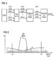
- FIG. 8 shows a frequency spectrum of the analog in relation to FIG Output signal AOUT.
- fOUT / fCLK plotted while vertical to the analog output signal AOUT assigned level values P are shown.
- interfering signals SS with the clock frequency fDATA and their Harmonics formed by crosstalk in the analog Output signal AOUT arrive.
- interfering signals with the frequency fDATA fCLK / NpL including theirs Harmonics formed at least partially in the Payload frequency range FB fall.
- the parallelized data signal DS with Help a ⁇ converter is formed is in the frequency spectrum FS still consider a noise spectrum RS of the ⁇ converter.
- the parallelized digital data signal into a serial data signal thus have the associated clock frequencies also Divider ratio, which includes the factor 4.
- Divider ratio which includes the factor 4.
- the above-described parallelized Data signal having NpL single data signals first parallelized data signal in a second parallelized Data signal converted with NpL 'individual data signals.
- both the first and the second parallelized Data signal a same, but compared to the arrangement as shown in FIG 7 increased clock frequency, which is advantageous different clock frequencies within the digital Circuit part can be avoided.
- first parallelized data signal In the first parallelized data signal are pauses in the Data transfer introduced, creating a discontinuous Data stream formed at the parallelized first data signal becomes. In doing so, individual data retain their positions in the data stream, a medium data rate is maintained. Depending on the implementation it is also possible during one clock cycle suppress a clock pulse of the increased clock frequency. It must be ensured in each case that during such Pausentakt no valid data of the parallelized first data signal to be transmitted. The pause clock occurs doing so randomly within a clock cycle.
- Method is used to form the serial data signal used demultiplexer formed multi-stage, whereby a improved noise reduction or suppression achieved becomes.
- a parallelized first data signal DS21 with an associated one Clock frequency fDATA2 is controlled by a digital signal processing device DSV1 formed.
- the serial digital output data signal formed by the demultiplexer DEMUX1 DOUT1 reaches the digital-to-analog converter DAW, which is an analog output signal AOUT1 in a through Frequencies fOUT1 covered frequency range forms.
- the divider ratio NpL ' is chosen to be NpL' ⁇ NpL such that that the divider ratio NpL 'no longer contains the factor 4, or that the divider ratio NpL 'by the factor 4 is not integer divisible.
- the device for clock and data rate adaptation TRA1 a total of 16 input data signals in a total of 15 output signals is in the digital signal processing device DSV1 and in the clock and data rate adaptation device TRA1 to avoid data overflow or loss of data within a 16-bar Clock cycle of the clock frequency fDATA2 once a pause of one To put in tact. During this pause cycle will be no transmit valid data of the parallelized first data signal. This will be described later with reference to FIGS. 3 and 4 described.
- the inventive method peak levels of Interference signals and their harmonics in the useful signal frequency band the analog output signal AOUT1 avoided or reduced.
- the implementation of the parallelized first data signal DS21 in the second data signal DS22 is using a in the Figures 3 and FIG 4 closer described cache carried out.
- the factor is for the clock increase 16/15 and thus corresponds to a minimum Clock frequency increase by 6.7%.
- the described in Figure 1 arrangement was for a serial Data flow DOUT1 described, which has a width of one bit having.
- the invention is also for an m-bit wide serial Data stream applicable, in which case m bits each Form a date that represents an analog value.
- the analog Values form the output of the digital / analog converter analogue output signal.
- m * NpL become parallel Single data signals of the digital signal processing device DSV1 converted to a total of m * NpL 'individual data signals.
- FIG. 2 shows, with reference to FIG. 1, a frequency spectrum of the analog Output signal AOUT1.
- AOUT1 a frequency spectrum of the analog Output signal AOUT1.
- fOUT1 / fCLK plotted while vertical to the analog Output level AOUT associated level values P shown are.
- so-called alias frequency spectra AS11 and AS12 of the useful signal NS1 are shown, which occur at the frequencies, 3/4 * fCLK, 5/4 * fCLK, ....
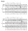
- FIG. 3 shows a data rate adaptation according to the invention used latches with exemplary occupancy.
- a FIFO memory First-In-First-Out, FIFO
- FIG Means arranged for clock and data rate adjustment TRA1.
- the FIFO memory has in the present Example for 16 digital input data signals in total fifteen columns, column 0 through column 14, and three rows row 1 to 3 on.
- data A7 to A15 are stored in column 0 to column 8, while data B0 to B5 are stored in column 9 to column 14.
- data B6 to B15 are stored in column 0 to column 9, while new data C0 to C4 are stored starting from the pointer position in column 10 to column 14.
- new data C5 to C15 are stored in column 0 to column 10.
- the pointer Z is moved one column to the right to a new one Position in line 2, column 11, moved.
- the memory state T10 changes to Memory state T11.
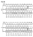
- FIG. 4 shows the buffer with a further exemplary Occupancy and with two introduced for data rate adjustment, randomly successive pause measures.
- all memory cells of the cache used.
- One clock cycle has 16 clocks each.
- the memory states T14 and T15 belong to the last two bars of a expiring clock cycle.
- Pausentakt PT occurs.
- data A3 to A15 are stored in column 0 to column 12, while data B0 and B1 are stored in column 13 and column 14.
- data B2 to B15 are stored in column 0 to column 13, while new data C0 are stored starting from the pointer position in column 14.
- new data C1 to C15 are stored in column 0 to column 14.
- the pointer Z is moved one column to the right to a new one Position in line 1, column 0, shifted.
- FIG. 5 shows an arrangement for carrying out the inventive Method with a multistage demultiplexer.
- a parallelized data signal DS3 is by a digital Signal processing device DSV3 formed.
- the parallelized Data signal DS3 has a total of 16 parallel to each other transmitted digital single data signals D300 to D315 on, to a device for clock and data rate adaptation TRA3 arrive.
- the device for clock and data rate adaptation TRA3 forms the total of 16 individual data signals D300 to D315 to a total of 15 individual data signals D400 to D414 from.
- the 15 individual data signals D400 to D414 form again parallelized data signal DS4, the one as a demultiplexer DEMUX3 trained parallel-parallel converter PPW3 arrives.
- both (clock) divider ratios with 5: 1 and with 3: 1 are chosen to be relatively small, since the overall divider ratio 15: 1 does not contain large prime factors.
- the last line of the buffer could be omitted without restriction in the pause selection when the output Z is accessed directly by means of the pointer Z.
- the divider ratio NpL ' is preferably selected such that it does not have large prime factors to reduce the overhead of the Minimize parallel-to-serial conversion.
- the divider ratio NpL 'starting at NpL-1 gradually decreasing to a value that neither contains the factor 4 integer and ideally none has too high a prime factor.
Landscapes
- Engineering & Computer Science (AREA)
- Power Engineering (AREA)
- Computer Networks & Wireless Communication (AREA)
- Signal Processing (AREA)
- Analogue/Digital Conversion (AREA)
- Synchronisation In Digital Transmission Systems (AREA)
Priority Applications (1)
| Application Number | Priority Date | Filing Date | Title |
|---|---|---|---|
| EP03026763.7A EP1533962B1 (fr) | 2003-11-21 | 2003-11-21 | Procédé et dispositif de suppression d'interférences dans la bande de fréquences utile d'un signal analogique de sortie |
Applications Claiming Priority (1)
| Application Number | Priority Date | Filing Date | Title |
|---|---|---|---|
| EP03026763.7A EP1533962B1 (fr) | 2003-11-21 | 2003-11-21 | Procédé et dispositif de suppression d'interférences dans la bande de fréquences utile d'un signal analogique de sortie |
Publications (2)
| Publication Number | Publication Date |
|---|---|
| EP1533962A1 true EP1533962A1 (fr) | 2005-05-25 |
| EP1533962B1 EP1533962B1 (fr) | 2015-11-11 |
Family
ID=34429410
Family Applications (1)
| Application Number | Title | Priority Date | Filing Date |
|---|---|---|---|
| EP03026763.7A Expired - Lifetime EP1533962B1 (fr) | 2003-11-21 | 2003-11-21 | Procédé et dispositif de suppression d'interférences dans la bande de fréquences utile d'un signal analogique de sortie |
Country Status (1)
| Country | Link |
|---|---|
| EP (1) | EP1533962B1 (fr) |
Cited By (1)
| Publication number | Priority date | Publication date | Assignee | Title |
|---|---|---|---|---|
| EP1868313A3 (fr) * | 2006-06-14 | 2008-05-21 | Siemens Aktiengesellschaft | Procédé destiné à la transmission de données entre un dispositif de commande à tête d'implantation de composants, automate d'implantation, tête d'implantation de composants, dispositif de transmission du côté émetteur et système pourvu du système de transmission des côtés émetteur et récepteur |
Citations (3)
| Publication number | Priority date | Publication date | Assignee | Title |
|---|---|---|---|---|
| EP0092083A2 (fr) * | 1982-04-17 | 1983-10-26 | Neumann Elektronik GmbH | Emetteur de messages électronique pour la transmission et/ou l'enregistrement de messages sur une ligne téléphonique |
| US4868572A (en) * | 1987-02-28 | 1989-09-19 | Alcatel N.V. | Circuit arrangement for converting digital sound-signal values into an analog sound signal |
| US5555447A (en) * | 1993-05-14 | 1996-09-10 | Motorola, Inc. | Method and apparatus for mitigating speech loss in a communication system |
-
2003
- 2003-11-21 EP EP03026763.7A patent/EP1533962B1/fr not_active Expired - Lifetime
Patent Citations (3)
| Publication number | Priority date | Publication date | Assignee | Title |
|---|---|---|---|---|
| EP0092083A2 (fr) * | 1982-04-17 | 1983-10-26 | Neumann Elektronik GmbH | Emetteur de messages électronique pour la transmission et/ou l'enregistrement de messages sur une ligne téléphonique |
| US4868572A (en) * | 1987-02-28 | 1989-09-19 | Alcatel N.V. | Circuit arrangement for converting digital sound-signal values into an analog sound signal |
| US5555447A (en) * | 1993-05-14 | 1996-09-10 | Motorola, Inc. | Method and apparatus for mitigating speech loss in a communication system |
Non-Patent Citations (2)
| Title |
|---|
| CAO J ET AL: "OC-192 transmitter and receiver in standard 0.18- mu m CMOS", IEEE JOURNAL OF SOLID-STATE CIRCUITS, vol. 37, no. 12, December 2002 (2002-12-01), IEEE,USA, pages 1768 - 1780, XP002288148, ISSN: 0018-9200 * |
| KAWAI T ET AL: "CROSSTALK REDUCTION IN N X N WDM MULTI/DEMULTIPLEXERS BY CASCADING SMALL ARRAYED WAVEGUIDE GRATING (AWG'S)", JOURNAL OF LIGHTWAVE TECHNOLOGY, vol. 15, no. 10, 1 October 1997 (1997-10-01), IEEE, NEW YORK, US, pages 1929 - 1937, XP000703612, ISSN: 0733-8724 * |
Cited By (1)
| Publication number | Priority date | Publication date | Assignee | Title |
|---|---|---|---|---|
| EP1868313A3 (fr) * | 2006-06-14 | 2008-05-21 | Siemens Aktiengesellschaft | Procédé destiné à la transmission de données entre un dispositif de commande à tête d'implantation de composants, automate d'implantation, tête d'implantation de composants, dispositif de transmission du côté émetteur et système pourvu du système de transmission des côtés émetteur et récepteur |
Also Published As
| Publication number | Publication date |
|---|---|
| EP1533962B1 (fr) | 2015-11-11 |
Similar Documents
| Publication | Publication Date | Title |
|---|---|---|
| DE3044208C2 (de) | Interpolator zur Erhöhung der Wortgeschwindigkeit eines digitalen Signals | |
| DE69017129T2 (de) | Frequenzsynthesizer mit gebrochenem teilverhältnis. | |
| DE69132757T2 (de) | Vorrichtung zu Parallelserien und zur Serienparallelwandlung von Daten und dadurch entstandenes serielles digitales Nachrichtenübertragungssystem | |
| DE69817270T2 (de) | Anordnung zur Erzeugung von analogen Signalen unter Benutzung von Analog-Digitalwandlern, besonders für direkte digitale Synthese | |
| DE4241882A1 (fr) | ||
| DE2605724C2 (de) | Digital-Analog-Umsetzer für PCM-codierte Digitalsignale | |
| DE68922930T2 (de) | Impulseinblendungsanordnung. | |
| DE69015946T2 (de) | Analog-Digitalwandler von hoher Umwandlungsfrequenz. | |
| DE3120669A1 (de) | A/d - und d/a - wandler | |
| DE10325839B4 (de) | Verfahren und Schaltung zur Crestfaktor-Reduzierung | |
| DE3813068C2 (de) | Einrichtung zur Verwendung als Filter in einem Digital/Analog-Konverter | |
| DE3810664C2 (fr) | ||
| DE4325728A1 (de) | Störreduktion für eine auf mehreren Modulatoren basierende Synthese | |
| EP0732823B1 (fr) | Méthode de récupération d'horloge d'un signal numérique à la réception | |
| DE3033914A1 (de) | Digital/analog-umsetzer und pcm-codierer damit. | |
| DE102005030563B4 (de) | Mehrkanal-Digital/Analog-Wandleranordnung | |
| EP1533962B1 (fr) | Procédé et dispositif de suppression d'interférences dans la bande de fréquences utile d'un signal analogique de sortie | |
| EP0340301A1 (fr) | Procede de codage numerique adaptatif par transformees | |
| DE69403549T2 (de) | Signalverarbeitungsanordnung mit mehreren verschiedenen Filtern, insbesondere für audiofrequente Codierung von Stimmensignalen | |
| DE2011772B2 (de) | Filter mit einer periodischen frequenzcharakteristik | |
| DE3230270C2 (de) | Verfahren zur zeitlichen Verschachtelung dreier Binärsignale | |
| DE2827958B1 (de) | Streckenregenerator fuer in einem Partial-Response-Code vorliegende mehrstufige digitale Signale | |
| DE2905080A1 (de) | Digitales zeitmultiplex-nachrichtenuebertragungssystem mit einzelkanal-kodierung/dekodierung | |
| DE10112275A1 (de) | Interpolator | |
| DE19716314A1 (de) | Verfahren und Vorrichtung zur Addition von als Abtastwerte vorliegenden Signalen |
Legal Events
| Date | Code | Title | Description |
|---|---|---|---|
| PUAI | Public reference made under article 153(3) epc to a published international application that has entered the european phase |
Free format text: ORIGINAL CODE: 0009012 |
|
| AK | Designated contracting states |
Kind code of ref document: A1 Designated state(s): AT BE BG CH CY CZ DE DK EE ES FI FR GB GR HU IE IT LI LU MC NL PT RO SE SI SK TR |
|
| AX | Request for extension of the european patent |
Extension state: AL LT LV MK |
|
| 17P | Request for examination filed |
Effective date: 20050620 |
|
| AKX | Designation fees paid |
Designated state(s): AT BE BG CH CY CZ DE DK EE ES FI FR GB GR HU IE IT LI LU MC NL PT RO SE SI SK TR |
|
| RAP1 | Party data changed (applicant data changed or rights of an application transferred) |
Owner name: NOKIA SIEMENS NETWORKS GMBH & CO. KG |
|
| RAP3 | Party data changed (applicant data changed or rights of an application transferred) |
Owner name: NOKIA SIEMENS NETWORKS S.P.A. |
|
| RAP3 | Party data changed (applicant data changed or rights of an application transferred) |
Owner name: NOKIA SIEMENS NETWORKS GMBH & CO. KG |
|
| RAP1 | Party data changed (applicant data changed or rights of an application transferred) |
Owner name: NOKIA SOLUTIONS AND NETWORKS GMBH & CO. KG |
|
| GRAP | Despatch of communication of intention to grant a patent |
Free format text: ORIGINAL CODE: EPIDOSNIGR1 |
|
| INTG | Intention to grant announced |
Effective date: 20150611 |
|
| GRAS | Grant fee paid |
Free format text: ORIGINAL CODE: EPIDOSNIGR3 |
|
| GRAA | (expected) grant |
Free format text: ORIGINAL CODE: 0009210 |
|
| AK | Designated contracting states |
Kind code of ref document: B1 Designated state(s): AT BE BG CH CY CZ DE DK EE ES FI FR GB GR HU IE IT LI LU MC NL PT RO SE SI SK TR |
|
| REG | Reference to a national code |
Ref country code: GB Ref legal event code: FG4D Free format text: NOT ENGLISH |
|
| REG | Reference to a national code |
Ref country code: CH Ref legal event code: EP |
|
| REG | Reference to a national code |
Ref country code: IE Ref legal event code: FG4D Free format text: LANGUAGE OF EP DOCUMENT: GERMAN |
|
| REG | Reference to a national code |
Ref country code: AT Ref legal event code: REF Ref document number: 760934 Country of ref document: AT Kind code of ref document: T Effective date: 20151215 |
|
| REG | Reference to a national code |
Ref country code: DE Ref legal event code: R096 Ref document number: 50315374 Country of ref document: DE |
|
| REG | Reference to a national code |
Ref country code: NL Ref legal event code: MP Effective date: 20160211 |
|
| PG25 | Lapsed in a contracting state [announced via postgrant information from national office to epo] |
Ref country code: IT Free format text: LAPSE BECAUSE OF FAILURE TO SUBMIT A TRANSLATION OF THE DESCRIPTION OR TO PAY THE FEE WITHIN THE PRESCRIBED TIME-LIMIT Effective date: 20151111 Ref country code: NL Free format text: LAPSE BECAUSE OF FAILURE TO SUBMIT A TRANSLATION OF THE DESCRIPTION OR TO PAY THE FEE WITHIN THE PRESCRIBED TIME-LIMIT Effective date: 20151111 Ref country code: ES Free format text: LAPSE BECAUSE OF FAILURE TO SUBMIT A TRANSLATION OF THE DESCRIPTION OR TO PAY THE FEE WITHIN THE PRESCRIBED TIME-LIMIT Effective date: 20151111 |
|
| PG25 | Lapsed in a contracting state [announced via postgrant information from national office to epo] |
Ref country code: SE Free format text: LAPSE BECAUSE OF FAILURE TO SUBMIT A TRANSLATION OF THE DESCRIPTION OR TO PAY THE FEE WITHIN THE PRESCRIBED TIME-LIMIT Effective date: 20151111 Ref country code: FI Free format text: LAPSE BECAUSE OF FAILURE TO SUBMIT A TRANSLATION OF THE DESCRIPTION OR TO PAY THE FEE WITHIN THE PRESCRIBED TIME-LIMIT Effective date: 20151111 Ref country code: PT Free format text: LAPSE BECAUSE OF FAILURE TO SUBMIT A TRANSLATION OF THE DESCRIPTION OR TO PAY THE FEE WITHIN THE PRESCRIBED TIME-LIMIT Effective date: 20160311 Ref country code: GR Free format text: LAPSE BECAUSE OF FAILURE TO SUBMIT A TRANSLATION OF THE DESCRIPTION OR TO PAY THE FEE WITHIN THE PRESCRIBED TIME-LIMIT Effective date: 20160212 Ref country code: BE Free format text: LAPSE BECAUSE OF NON-PAYMENT OF DUE FEES Effective date: 20151130 |
|
| REG | Reference to a national code |
Ref country code: CH Ref legal event code: PL |
|
| PG25 | Lapsed in a contracting state [announced via postgrant information from national office to epo] |
Ref country code: CH Free format text: LAPSE BECAUSE OF NON-PAYMENT OF DUE FEES Effective date: 20151130 Ref country code: CZ Free format text: LAPSE BECAUSE OF FAILURE TO SUBMIT A TRANSLATION OF THE DESCRIPTION OR TO PAY THE FEE WITHIN THE PRESCRIBED TIME-LIMIT Effective date: 20151111 Ref country code: LI Free format text: LAPSE BECAUSE OF NON-PAYMENT OF DUE FEES Effective date: 20151130 |
|
| REG | Reference to a national code |
Ref country code: DE Ref legal event code: R097 Ref document number: 50315374 Country of ref document: DE |
|
| REG | Reference to a national code |
Ref country code: IE Ref legal event code: MM4A |
|
| PG25 | Lapsed in a contracting state [announced via postgrant information from national office to epo] |
Ref country code: SK Free format text: LAPSE BECAUSE OF FAILURE TO SUBMIT A TRANSLATION OF THE DESCRIPTION OR TO PAY THE FEE WITHIN THE PRESCRIBED TIME-LIMIT Effective date: 20151111 Ref country code: RO Free format text: LAPSE BECAUSE OF FAILURE TO SUBMIT A TRANSLATION OF THE DESCRIPTION OR TO PAY THE FEE WITHIN THE PRESCRIBED TIME-LIMIT Effective date: 20151111 Ref country code: DK Free format text: LAPSE BECAUSE OF FAILURE TO SUBMIT A TRANSLATION OF THE DESCRIPTION OR TO PAY THE FEE WITHIN THE PRESCRIBED TIME-LIMIT Effective date: 20151111 Ref country code: EE Free format text: LAPSE BECAUSE OF FAILURE TO SUBMIT A TRANSLATION OF THE DESCRIPTION OR TO PAY THE FEE WITHIN THE PRESCRIBED TIME-LIMIT Effective date: 20151111 |
|
| PLBE | No opposition filed within time limit |
Free format text: ORIGINAL CODE: 0009261 |
|
| STAA | Information on the status of an ep patent application or granted ep patent |
Free format text: STATUS: NO OPPOSITION FILED WITHIN TIME LIMIT |
|
| PG25 | Lapsed in a contracting state [announced via postgrant information from national office to epo] |
Ref country code: MC Free format text: LAPSE BECAUSE OF FAILURE TO SUBMIT A TRANSLATION OF THE DESCRIPTION OR TO PAY THE FEE WITHIN THE PRESCRIBED TIME-LIMIT Effective date: 20151111 |
|
| 26N | No opposition filed |
Effective date: 20160812 |
|
| PG25 | Lapsed in a contracting state [announced via postgrant information from national office to epo] |
Ref country code: IE Free format text: LAPSE BECAUSE OF NON-PAYMENT OF DUE FEES Effective date: 20151121 |
|
| REG | Reference to a national code |
Ref country code: FR Ref legal event code: ST Effective date: 20161003 |
|
| PG25 | Lapsed in a contracting state [announced via postgrant information from national office to epo] |
Ref country code: FR Free format text: LAPSE BECAUSE OF NON-PAYMENT OF DUE FEES Effective date: 20160111 Ref country code: SI Free format text: LAPSE BECAUSE OF FAILURE TO SUBMIT A TRANSLATION OF THE DESCRIPTION OR TO PAY THE FEE WITHIN THE PRESCRIBED TIME-LIMIT Effective date: 20151111 |
|
| REG | Reference to a national code |
Ref country code: AT Ref legal event code: MM01 Ref document number: 760934 Country of ref document: AT Kind code of ref document: T Effective date: 20151121 |
|
| PG25 | Lapsed in a contracting state [announced via postgrant information from national office to epo] |
Ref country code: AT Free format text: LAPSE BECAUSE OF NON-PAYMENT OF DUE FEES Effective date: 20151121 |
|
| PG25 | Lapsed in a contracting state [announced via postgrant information from national office to epo] |
Ref country code: HU Free format text: LAPSE BECAUSE OF FAILURE TO SUBMIT A TRANSLATION OF THE DESCRIPTION OR TO PAY THE FEE WITHIN THE PRESCRIBED TIME-LIMIT; INVALID AB INITIO Effective date: 20031121 Ref country code: BG Free format text: LAPSE BECAUSE OF FAILURE TO SUBMIT A TRANSLATION OF THE DESCRIPTION OR TO PAY THE FEE WITHIN THE PRESCRIBED TIME-LIMIT Effective date: 20151111 |
|
| PG25 | Lapsed in a contracting state [announced via postgrant information from national office to epo] |
Ref country code: CY Free format text: LAPSE BECAUSE OF FAILURE TO SUBMIT A TRANSLATION OF THE DESCRIPTION OR TO PAY THE FEE WITHIN THE PRESCRIBED TIME-LIMIT Effective date: 20151111 |
|
| PG25 | Lapsed in a contracting state [announced via postgrant information from national office to epo] |
Ref country code: TR Free format text: LAPSE BECAUSE OF FAILURE TO SUBMIT A TRANSLATION OF THE DESCRIPTION OR TO PAY THE FEE WITHIN THE PRESCRIBED TIME-LIMIT Effective date: 20151111 |
|
| PG25 | Lapsed in a contracting state [announced via postgrant information from national office to epo] |
Ref country code: LU Free format text: LAPSE BECAUSE OF NON-PAYMENT OF DUE FEES Effective date: 20151121 |
|
| PGFP | Annual fee paid to national office [announced via postgrant information from national office to epo] |
Ref country code: DE Payment date: 20171121 Year of fee payment: 15 |
|
| PGFP | Annual fee paid to national office [announced via postgrant information from national office to epo] |
Ref country code: GB Payment date: 20171123 Year of fee payment: 15 |
|
| REG | Reference to a national code |
Ref country code: GB Ref legal event code: 732E Free format text: REGISTERED BETWEEN 20190207 AND 20190213 |
|
| REG | Reference to a national code |
Ref country code: DE Ref legal event code: R081 Ref document number: 50315374 Country of ref document: DE Owner name: PROVENANCE ASSET GROUP LLC, PITTSFORD, US Free format text: FORMER OWNER: NOKIA SOLUTIONS AND NETWORKS GMBH & CO. KG, 81541 MUENCHEN, DE |
|
| REG | Reference to a national code |
Ref country code: DE Ref legal event code: R119 Ref document number: 50315374 Country of ref document: DE |
|
| GBPC | Gb: european patent ceased through non-payment of renewal fee |
Effective date: 20181121 |
|
| PG25 | Lapsed in a contracting state [announced via postgrant information from national office to epo] |
Ref country code: DE Free format text: LAPSE BECAUSE OF NON-PAYMENT OF DUE FEES Effective date: 20190601 |
|
| PG25 | Lapsed in a contracting state [announced via postgrant information from national office to epo] |
Ref country code: GB Free format text: LAPSE BECAUSE OF NON-PAYMENT OF DUE FEES Effective date: 20181121 |