EP1535730A1 - Schichtenfolge zur Herstellung eines Verbundmaterials für elektromechanische Bauelemente - Google Patents
Schichtenfolge zur Herstellung eines Verbundmaterials für elektromechanische Bauelemente Download PDFInfo
- Publication number
- EP1535730A1 EP1535730A1 EP04023558A EP04023558A EP1535730A1 EP 1535730 A1 EP1535730 A1 EP 1535730A1 EP 04023558 A EP04023558 A EP 04023558A EP 04023558 A EP04023558 A EP 04023558A EP 1535730 A1 EP1535730 A1 EP 1535730A1
- Authority
- EP
- European Patent Office
- Prior art keywords
- layer
- substrate
- thickness
- copper
- barrier
- Prior art date
- Legal status (The legal status is an assumption and is not a legal conclusion. Google has not performed a legal analysis and makes no representation as to the accuracy of the status listed.)
- Granted
Links
Images
Classifications
-
- H—ELECTRICITY
- H05—ELECTRIC TECHNIQUES NOT OTHERWISE PROVIDED FOR
- H05K—PRINTED CIRCUITS; CASINGS OR CONSTRUCTIONAL DETAILS OF ELECTRIC APPARATUS; MANUFACTURE OF ASSEMBLAGES OF ELECTRICAL COMPONENTS
- H05K3/00—Apparatus or processes for manufacturing printed circuits
- H05K3/22—Secondary treatment of printed circuits
- H05K3/24—Reinforcing of the conductive pattern
- H05K3/244—Finish plating of conductors, especially of copper conductors, e.g. for pads or lands
-
- B—PERFORMING OPERATIONS; TRANSPORTING
- B32—LAYERED PRODUCTS
- B32B—LAYERED PRODUCTS, i.e. PRODUCTS BUILT-UP OF STRATA OF FLAT OR NON-FLAT, e.g. CELLULAR OR HONEYCOMB, FORM
- B32B15/00—Layered products comprising a layer of metal
- B32B15/01—Layered products comprising a layer of metal all layers being exclusively metallic
- B32B15/018—Layered products comprising a layer of metal all layers being exclusively metallic one layer being formed of a noble metal or a noble metal alloy
-
- C—CHEMISTRY; METALLURGY
- C23—COATING METALLIC MATERIAL; COATING MATERIAL WITH METALLIC MATERIAL; CHEMICAL SURFACE TREATMENT; DIFFUSION TREATMENT OF METALLIC MATERIAL; COATING BY VACUUM EVAPORATION, BY SPUTTERING, BY ION IMPLANTATION OR BY CHEMICAL VAPOUR DEPOSITION, IN GENERAL; INHIBITING CORROSION OF METALLIC MATERIAL OR INCRUSTATION IN GENERAL
- C23C—COATING METALLIC MATERIAL; COATING MATERIAL WITH METALLIC MATERIAL; SURFACE TREATMENT OF METALLIC MATERIAL BY DIFFUSION INTO THE SURFACE, BY CHEMICAL CONVERSION OR SUBSTITUTION; COATING BY VACUUM EVAPORATION, BY SPUTTERING, BY ION IMPLANTATION OR BY CHEMICAL VAPOUR DEPOSITION, IN GENERAL
- C23C26/00—Coating not provided for in groups C23C2/00 - C23C24/00
-
- C—CHEMISTRY; METALLURGY
- C23—COATING METALLIC MATERIAL; COATING MATERIAL WITH METALLIC MATERIAL; CHEMICAL SURFACE TREATMENT; DIFFUSION TREATMENT OF METALLIC MATERIAL; COATING BY VACUUM EVAPORATION, BY SPUTTERING, BY ION IMPLANTATION OR BY CHEMICAL VAPOUR DEPOSITION, IN GENERAL; INHIBITING CORROSION OF METALLIC MATERIAL OR INCRUSTATION IN GENERAL
- C23C—COATING METALLIC MATERIAL; COATING MATERIAL WITH METALLIC MATERIAL; SURFACE TREATMENT OF METALLIC MATERIAL BY DIFFUSION INTO THE SURFACE, BY CHEMICAL CONVERSION OR SUBSTITUTION; COATING BY VACUUM EVAPORATION, BY SPUTTERING, BY ION IMPLANTATION OR BY CHEMICAL VAPOUR DEPOSITION, IN GENERAL
- C23C28/00—Coating for obtaining at least two superposed coatings either by methods not provided for in a single one of groups C23C2/00 - C23C26/00 or by combinations of methods provided for in subclasses C23C and C25C or C25D
- C23C28/02—Coating for obtaining at least two superposed coatings either by methods not provided for in a single one of groups C23C2/00 - C23C26/00 or by combinations of methods provided for in subclasses C23C and C25C or C25D only coatings only including layers of metallic material
- C23C28/021—Coating for obtaining at least two superposed coatings either by methods not provided for in a single one of groups C23C2/00 - C23C26/00 or by combinations of methods provided for in subclasses C23C and C25C or C25D only coatings only including layers of metallic material including at least one metal alloy layer
-
- C—CHEMISTRY; METALLURGY
- C23—COATING METALLIC MATERIAL; COATING MATERIAL WITH METALLIC MATERIAL; CHEMICAL SURFACE TREATMENT; DIFFUSION TREATMENT OF METALLIC MATERIAL; COATING BY VACUUM EVAPORATION, BY SPUTTERING, BY ION IMPLANTATION OR BY CHEMICAL VAPOUR DEPOSITION, IN GENERAL; INHIBITING CORROSION OF METALLIC MATERIAL OR INCRUSTATION IN GENERAL
- C23C—COATING METALLIC MATERIAL; COATING MATERIAL WITH METALLIC MATERIAL; SURFACE TREATMENT OF METALLIC MATERIAL BY DIFFUSION INTO THE SURFACE, BY CHEMICAL CONVERSION OR SUBSTITUTION; COATING BY VACUUM EVAPORATION, BY SPUTTERING, BY ION IMPLANTATION OR BY CHEMICAL VAPOUR DEPOSITION, IN GENERAL
- C23C28/00—Coating for obtaining at least two superposed coatings either by methods not provided for in a single one of groups C23C2/00 - C23C26/00 or by combinations of methods provided for in subclasses C23C and C25C or C25D
- C23C28/02—Coating for obtaining at least two superposed coatings either by methods not provided for in a single one of groups C23C2/00 - C23C26/00 or by combinations of methods provided for in subclasses C23C and C25C or C25D only coatings only including layers of metallic material
- C23C28/023—Coating for obtaining at least two superposed coatings either by methods not provided for in a single one of groups C23C2/00 - C23C26/00 or by combinations of methods provided for in subclasses C23C and C25C or C25D only coatings only including layers of metallic material only coatings of metal elements only
-
- H—ELECTRICITY
- H01—ELECTRIC ELEMENTS
- H01R—ELECTRICALLY-CONDUCTIVE CONNECTIONS; STRUCTURAL ASSOCIATIONS OF A PLURALITY OF MUTUALLY-INSULATED ELECTRICAL CONNECTING ELEMENTS; COUPLING DEVICES; CURRENT COLLECTORS
- H01R13/00—Details of coupling devices of the kinds covered by groups H01R12/70 or H01R24/00 - H01R33/00
- H01R13/02—Contact members
- H01R13/03—Contact members characterised by the material, e.g. plating, or coating materials
-
- H—ELECTRICITY
- H10—SEMICONDUCTOR DEVICES; ELECTRIC SOLID-STATE DEVICES NOT OTHERWISE PROVIDED FOR
- H10W—GENERIC PACKAGES, INTERCONNECTIONS, CONNECTORS OR OTHER CONSTRUCTIONAL DETAILS OF DEVICES COVERED BY CLASS H10
- H10W70/00—Package substrates; Interposers; Redistribution layers [RDL]
- H10W70/20—Conductive package substrates serving as an interconnection, e.g. metal plates
- H10W70/24—Conductive package substrates serving as an interconnection, e.g. metal plates characterised by materials
Definitions
- the invention relates to a layer sequence on a copper or a substrate Copper-based alloy, of nickel or a nickel-based alloy or a copper-plated substrate for producing a composite material and a method for producing a composite material from the layer sequence.
- intermetallic phases such as Cu 3 Sn, Cu 6 Sn 5 or Ni 3 Sn are formed as a result of diffusion processes.
- the iron barrier layer used forms a FeSn 2 -IMP at temperatures of 170 ° C.
- the thickness growth is correspondingly low, whereby an effective barrier to the diffusion of Sn is only given, as long as it is free of pores.
- a Cu 6 Sn 5 IMP forms below the Fe layer, causing the Fe barrier layer to flake off the base material.
- Pore-dense layers can only be achieved from about 2 ⁇ m layer thickness. Since, in particular, relatively thick Fe layers can cause problems due to the magnetic properties in the electronics industry, so far in practice this has been abandoned.
- the invention is therefore based on the object, in particular for Tin coatings, the adhesion of the layer also to long-term temperature outsourcing sustainably improve and the layer properties too stabilize.
- the invention is with respect to the layer sequence for producing a Composite material by the features of claim 1, with respect to the method for producing the composite material by the features of claim 9 played.
- the other claims give advantageous education and Further developments of the invention.
- the invention includes the technical teaching relating to a layer sequence a substrate made of copper or a copper-based alloy, nickel or a Nickel-based alloy or a copper-plated substrate for the production of a Composite material, wherein a cover layer consisting of tin or a Tin-based alloy disposed over at least a portion of the substrate is, a barrier layer that lies between the substrate and the cover layer and with the substrate is in direct contact, wherein the barrier layer of at least is an element of the group Fe, Co, Nb, Mo or Ta, and one Interlayer, which lies between the barrier layer and the cover layer and with the barrier layer is in direct contact, wherein the intermediate layer of consists of at least one element of the group Cu or Ni and a Reaction layer, which lies between cover layer and intermediate layer and from Ag or an Ag alloy composed of Pt or Pd or its alloys.
- the invention is based on the consideration that between the cover layer and the substrate further layers are introduced.
- the outermost layer of the Layer composite is pure Sn or a Sn alloy, depending on Application is selected.
- an Sn-based alloy from 0 to 50 wt.% Sn and from one or more of the elements Ag, Cu, Ni, In, Co, Bi, Pb and Sb.
- the mentioned Elements of the barrier layer can also be used in the form of an alloy.
- a multi-layer sequence such as a combination of Fe and Co or Ta and Co, is conceivable.
- the layers are on copper or a Cu alloy, applied to a copper-plated component as a substrate.
- the barrier layer consists of the mentioned pure elements or of a mixture thereof.
- the reaction layer which consists of Ag, Pd or Pt or their alloys, reacts at high temperatures with the top layer and depending on the thickness with the intermediate layer to an intermetallic phase. This is for example the Case, when the reaction layer of Ag and the covering layer of Sn or his Alloys exists. Depending on the thickness of the reaction and cover layer thus takes place a finishing and curing of the top layer instead, without the adhesive strength in the Use under temperature load is at risk.
- the Sn diffusing through the reaction layer and intermediate layer is attached to the Barrier layer by the reaction, for example with Fe, to another intermetallic phase tied, which further progress of the reaction stops.
- This will be very efficient for the service life of up to 3000 h and Temperatures up to 200 ° C, the formation of intermetallic phases of Cu and Sn is prevented at the interface with the substrate.
- the barrier layer may have a thickness from 0.2 to 1.0 ⁇ m. Layer thicknesses in this area can either so be called galvanic flash layers or layers that by means of PVD or CVD processes are deposited.
- the intermediate layer of either one Cu-Ni alloy or a layer sequence of a Ni and a Cu layer consist.
- the intermediate layer has a thickness of 0.2 - 2.0 ⁇ m. At lower layer thicknesses there is a risk that elements diffuse from the barrier to the surface and undesirably bad lead conductive corrosion products.
- the desired Sn layer can then be galvanically applied to these base coats be deposited.
- the cover layer has a larger one Thickness than the reaction layer on. Because part of the Sn layer is covered by a In any case, the subsequent heat treatment is used up be that the remaining thickness of the Sn cover layer is still complete Covering the surface is sufficient.
- the reaction layer has advantageously a layer thickness which corresponds to between 1/3 and 1/1 of the thickness of the cover layer, for example, to ensure at a ratio of 1: 3 that after 1000 h at 200 ° C still free Sn remains on the surface; at a ratio of 1: 1 the entire Sn layer is refined into an IMP with the reaction layer.
- a optimal coordination of the entire composite layer is in the above Thickness range.
- Layer thicknesses above the specified range are not required to achieve the desired effect in conjunction with a barrier layer achieve.
- the execution in the layer thickness ratio 1: 1 allows the simple and cost-effective production of SnAg or SnAgCu surfaces after one Reflow treatment, which has good electrical and mechanical properties exhibit.
- the reaction layer may have a greater thickness than that Have barrier layer and the intermediate layer.
- the layer thicknesses of the selected materials are lower required, as in the consuming reaction layer.
- the intermediate layer inhibits with the reaction layer, the Sn diffusion to the base material already in a considerable extent, so that a staking on the barrier layer also share with a small barrier layer thickness is sufficient, the further diffusion of tin in to prevent the substrate.
- the total layer thickness on the substrate is less than 12 ⁇ m, preferably less than 3 microns.
- these layer thicknesses cause a durable and reliable Sn coating of a copper or copper substrate a copper alloy or a copper-plated substrate.
- at least one layer is a galvanic layer, PVD or CVD layer.
- Substrate with barrier layer, interlayer and reaction layer and Sn layer so can be subjected to a conventional reflow treatment to the to achieve mutual diffusion bonding of the layers.
- the stratification of the network to be formed is sufficient heated for a long time above the melting temperature of the cover layer and then cooled.
- a successful reflow treatment is between Sn layer and Reaction layer interdiffusion occurred, leading to the formation of some Extent of desired AgSn intermetallic phases.
- the Adhesion of the barrier layer on the substrate and within the laminate improved.
- a composite material produced in this way is now emerging characterized in that at temperatures up to 200 ° C after up to 3000 h no Peeling effects are observed by vacancy condensation.
- the heat treatment in oil be performed.
- the reflow treatment are controlled evenly and selectively.
- tin layers can be self-lubricating Set properties.
- Composite material is preferably suitable for electromechanical components, Leadframes and rigid and flexible circuit boards.
- an effective barrier layer for Sn layers indicate after long-term temperature swapping, consist in particular that it does not come to flaking the entire layer and at the same time one effective protection against abrasion.
- Further advantageous properties of layers according to the invention are a low contact resistance, Corrosion resistance and good solderability.
- a high-gloss Sn layer the special resistant to fretting corrosion.
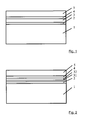
- the layer sequence of FIG. 1 is on a substrate 1 made of copper or a Copper-based alloy deposited.
- the cover layer 5 is made of tin or a Tin-based alloy that only partially covers the surface or, as in the Figure shown, is arranged area-wide.
- the barrier layer 2 is connected to the Substrate 1 in direct contact.
- the materials for the barrier layer 2 are made of the group Fe, Co, Nb, Mo or Ta.
- Between the cover layer 5 and the Barrier layer 2 is the intermediate layer 3 and the reaction layer 4, wherein the intermediate layer 3 in the example of a Cu / Ni alloy with a Proportion of up to 40 wt .-% Ni consists.
- the reaction layer has a thickness, which corresponds to about 1/3 of the thickness of the cover layer (5).
- Fig. 2 shows substantially the same layer sequence on the substrate 1 with the Difference that the intermediate layer 3 two layers of nickel and copper is trained.
- the Nickel layer 31 on the one hand in direct contact with the barrier layer 2, the On the other hand, copper layer 32 is in contact with the reaction layer 4, which consists of Ag.
- a strip 0.2 ⁇ 32 mm made of the Cu alloy C7025 (CuNi3Si1Mg) is coated with the layer sequence according to the invention.
- a Fe-Flash of 0.5 microns thickness is applied to the belt with a Galvanikstrom. So-called flash layers are deposits with a relatively small layer thickness.
- a nickel layer of 0.6 microns and then again a Cu-Flash of 0.2 microns thickness deposited.
- the reaction layer is a 0.5 .mu.m Ag layer and the last layer is a pure Sn layer of 1.0 micron thickness deposited and subjected to the layer composite of a reflow treatment.
- the ribbon-shaped composite material obtained is again stored at 125 ° C. and at 150 ° C. and examined at certain intervals. It is found that in contrast to the known method of the prior art at 150 ° C after 1000 h no detachment by peeling are observed. The swallows continued for up to 3,000 hours, but no signs of exfoliation were noted.
- the desired durability of the tin-plating can be achieved by the layer structure according to the invention.
- the formation of the SnAg 3 -IMP also keeps the contact resistance at a stable low level.
Landscapes
- Chemical & Material Sciences (AREA)
- Engineering & Computer Science (AREA)
- Organic Chemistry (AREA)
- Chemical Kinetics & Catalysis (AREA)
- Materials Engineering (AREA)
- Mechanical Engineering (AREA)
- Metallurgy (AREA)
- Microelectronics & Electronic Packaging (AREA)
- Manufacturing & Machinery (AREA)
- Laminated Bodies (AREA)
- Electroplating Methods And Accessories (AREA)
- Parts Printed On Printed Circuit Boards (AREA)
- Other Surface Treatments For Metallic Materials (AREA)
- Contacts (AREA)
- Ceramic Products (AREA)
- Glass Compositions (AREA)
Abstract
Description
- Fig. 1
- eine Schichtenfolge auf einem Substrat, und
- Fig. 2
- eine erfindungsgemäße Schichtenfolge mit zweilagiger Reaktionsschicht.
Ein Band 0,2 x 32 mm aus der Cu-Legierung C7025 (CuNi3Si1Mg) wird mit der erfindungsgemäßen Schichtenfolge beschichtet. Hierzu wird auf das Band mit einer Galvanikanlage ein Fe-Flash von 0,5 µm Dicke aufgebracht. So genannte Flashschichten sind Abscheidungen mit verhältnismäßig geringer Schichtdicke. Darauf wird eine Nickelschicht von 0,6 µm und darauf wiederum ein Cu-Flash von 0,2 µm Dicke abgeschieden. Als Reaktionsschicht dient eine 0,5 µm Ag-Schicht und als letzte Schicht wird eine reine Sn-Schicht von 1,0 µm Dicke abgeschieden und der Schichtverbund einer Reflow-Behandlung unterzogen.
Dabei stellt man fest, dass im Unterschied zu dem bekannten Verfahren des Standes der Technik bei 150 °C nach 1000 h keine Ablösungen durch Peeling beobachtet werden. Die Auslagerungen wurden bis zu 3000 h fortgesetzt, jedoch keine Anzeichen für Peeling festgestellt.
- 1
- Substrat
- 2
- Sperrschicht
- 3
- Zwischenschicht, Legierung
- 31
- Zwischenschicht, erste Schicht
- 32
- Zwischenschicht, zweite Schicht
- 4
- Reaktionsschicht
- 5
- Deckschicht
Claims (12)
- Schichtenfolge auf einem Substrat (1) aus Kupfer oder einer Kupferbasislegierung, aus Nickel oder einer Nickelbasislegierung oder eines verkupferten Substrates zur Herstellung eines Verbundmaterials, gekennzeichnet durch:eine Deckschicht (5), bestehend aus Zinn oder einer Legierung auf Zinnbasis, die zumindest über einem Teil des Substrates (1) angeordnet ist,eine Sperrschicht (2), die zwischen dem Substrat (1) und der Deckschicht (5) liegt und mit dem Substrat (1) unmittelbar in Kontakt steht, wobei die Sperrschicht (2) aus zumindest einem Element der Gruppe Fe, Co, Nb, Mo oder Ta besteht, undeine Zwischenschicht (3, 31,32), die zwischen der Sperrschicht (2) und der Deckschicht (5) liegt und mit der Sperrschicht (2) unmittelbar in Kontakt steht, wobei die Zwischenschicht (3, 31, 32) aus zumindest einem Element der Gruppe Cu oder Ni besteht.eine Reaktionsschicht (4), die zwischen Deckschicht (5) und Zwischenschicht (3) liegt und aus Ag oder einer Ag-Legierung, aus Pt oder Pd oder seinen Legierungen besteht.
- Schichtenfolge nach Anspruch 1, dadurch gekennzeichnet, dass die Sperrschicht (2) eine Dicke von 0,2 - 1,0 µm besitzt.
- Schichtenfolge nach Anspruch 1 oder 2, dadurch gekennzeichnet, dass die Zwischenschicht (3, 31, 32) eine Cu-Ni-Legierung oder eine Schichtenfolge einer Ni- und einer Cu-Schicht ist.
- Schichtenfolge nach Anspruch 3, dadurch gekennzeichnet, dass die Zwischenschicht (3, 31, 32) eine Dicke von 0,2 - 2,0 µm aufweist.
- Schichtenfolge nach einem der Ansprüche 1 bis 4, dadurch gekennzeichnet, dass die Reaktionsschicht (4) eine Dicke aufweist, welche zwischen 1/3 bis 1/1 der Dicke der Deckschicht (5) entspricht.
- Schichtenfolge nach einem der Ansprüche 1 bis 5, dadurch gekennzeichnet, dass die Reaktionsschicht (4) eine größere Dicke als die Sperrschicht (2) und die Zwischenschicht (3, 31, 32) aufweist.
- Schichtenfolge nach einem der Ansprüche 1 bis 6, dadurch gekennzeichnet, dass die gesamte Schichtdicke auf dem Substrat (1) geringer als 12 µm, vorzugsweise geringer als 3 µm ist.
- Schichtenfolge nach einem der vorstehenden Ansprüche, dadurch gekennzeichnet, dass es sich bei zumindest einer Schicht um eine Galvanikschicht, einer PVD- oder CVD-Schicht handelt.
- Verfahren zur Herstellung eines Verbundmaterials aus der Schichtenfolge nach einem der Ansprüche 1 bis 8, gekennzeichnet durch eine Wärmebehandlung der Schichtenfolge über der Schmelztemperatur der Deckschicht (5).
- Verfahren zur Herstellung eines Verbundmaterials aus der Schichtenfolge nach Anspruch 9, dadurch gekennzeichnet, dass die Wärmebehandlung in Öl, insbesondere in Parafinöl oder Esteröl, durchgeführt wird.
- Verbundmaterial, hergestellt nach dem Verfahren nach Anspruch 9 oder 10.
- Verwendung des Verbundmaterials nach Anspruch 11 für elektromechanische Bauelemente, Leadframes und starr und flexiblen Leiterplatten.
Priority Applications (3)
| Application Number | Priority Date | Filing Date | Title |
|---|---|---|---|
| JP2004335846A JP4739734B2 (ja) | 2003-11-28 | 2004-11-19 | 電子機械的構成要素用の複合材を製造するための連続層、その複合材及び使用方法 |
| US10/996,681 US7189630B2 (en) | 2003-11-28 | 2004-11-24 | Layer sequence for producing a composite material for electromechanical components |
| CN200410096264.8A CN1701952B (zh) | 2003-11-28 | 2004-11-26 | 用来制备用于电机构件的复合材料层结构 |
Applications Claiming Priority (2)
| Application Number | Priority Date | Filing Date | Title |
|---|---|---|---|
| DE10355724 | 2003-11-28 | ||
| DE10355724 | 2003-11-28 |
Publications (2)
| Publication Number | Publication Date |
|---|---|
| EP1535730A1 true EP1535730A1 (de) | 2005-06-01 |
| EP1535730B1 EP1535730B1 (de) | 2010-03-17 |
Family
ID=34442337
Family Applications (1)
| Application Number | Title | Priority Date | Filing Date |
|---|---|---|---|
| EP04023558A Expired - Lifetime EP1535730B1 (de) | 2003-11-28 | 2004-10-04 | Schichtenfolge zur Herstellung eines Verbundmaterials für elektromechanische Bauelemente |
Country Status (5)
| Country | Link |
|---|---|
| EP (1) | EP1535730B1 (de) |
| CN (1) | CN1701952B (de) |
| AT (1) | ATE461037T1 (de) |
| DE (1) | DE502004010902D1 (de) |
| ES (1) | ES2340161T3 (de) |
Cited By (2)
| Publication number | Priority date | Publication date | Assignee | Title |
|---|---|---|---|---|
| EP1898463A4 (de) * | 2005-05-23 | 2010-09-15 | Neomax Materials Co Ltd | Cu-Mo-SUBSTRAT UND VERFAHREN ZU SEINER HERSTELLUNG |
| DE102011078546A1 (de) * | 2011-07-01 | 2013-01-03 | Tyco Electronics Amp Gmbh | Elektrische Kontaktbeschichtung |
Families Citing this family (4)
| Publication number | Priority date | Publication date | Assignee | Title |
|---|---|---|---|---|
| TWI347643B (en) | 2007-06-13 | 2011-08-21 | Advanced Semiconductor Eng | Under bump metallurgy structure and die structure using the same and method of manufacturing die structure |
| JP6050664B2 (ja) * | 2012-06-27 | 2016-12-21 | Jx金属株式会社 | 電子部品用金属材料及びその製造方法、それを用いたコネクタ端子、コネクタ及び電子部品 |
| DE102020205537A1 (de) * | 2020-04-30 | 2021-11-04 | Robert Bosch Gesellschaft mit beschränkter Haftung | Verschleißschutzbeschichtetes Bauteil sowie Verfahren zum Beschichten desselben |
| KR102850769B1 (ko) * | 2023-08-18 | 2025-08-26 | 덕산하이메탈(주) | 연결핀 |
Citations (6)
| Publication number | Priority date | Publication date | Assignee | Title |
|---|---|---|---|---|
| DE3712691C1 (en) * | 1987-04-14 | 1988-06-23 | Prym Werke William | Electrical connecting pin, especially a coil former pin, and a method for its production |
| JPH10284667A (ja) * | 1997-04-04 | 1998-10-23 | Furukawa Electric Co Ltd:The | 耐食性、耐酸化性に優れる電気電子機器用部品材料、及びその製造方法 |
| US5916695A (en) * | 1995-12-18 | 1999-06-29 | Olin Corporation | Tin coated electrical connector |
| US6083633A (en) * | 1997-06-16 | 2000-07-04 | Olin Corporation | Multi-layer diffusion barrier for a tin coated electrical connector |
| US20030035977A1 (en) * | 2000-12-11 | 2003-02-20 | Amit Datta | Barrier layer for electrical connectors and methods of applying the layer |
| US20030091855A1 (en) * | 2001-01-19 | 2003-05-15 | Hitoshi Tanaka | Plated material, method of producing same, and electrical/electronic part using same |
Family Cites Families (1)
| Publication number | Priority date | Publication date | Assignee | Title |
|---|---|---|---|---|
| US5939212A (en) * | 1997-06-09 | 1999-08-17 | Atd Corporation | Flexible corrugated multilayer metal foil shields and method of making |
-
2004
- 2004-10-04 AT AT04023558T patent/ATE461037T1/de not_active IP Right Cessation
- 2004-10-04 EP EP04023558A patent/EP1535730B1/de not_active Expired - Lifetime
- 2004-10-04 ES ES04023558T patent/ES2340161T3/es not_active Expired - Lifetime
- 2004-10-04 DE DE502004010902T patent/DE502004010902D1/de not_active Expired - Lifetime
- 2004-11-26 CN CN200410096264.8A patent/CN1701952B/zh not_active Expired - Fee Related
Patent Citations (6)
| Publication number | Priority date | Publication date | Assignee | Title |
|---|---|---|---|---|
| DE3712691C1 (en) * | 1987-04-14 | 1988-06-23 | Prym Werke William | Electrical connecting pin, especially a coil former pin, and a method for its production |
| US5916695A (en) * | 1995-12-18 | 1999-06-29 | Olin Corporation | Tin coated electrical connector |
| JPH10284667A (ja) * | 1997-04-04 | 1998-10-23 | Furukawa Electric Co Ltd:The | 耐食性、耐酸化性に優れる電気電子機器用部品材料、及びその製造方法 |
| US6083633A (en) * | 1997-06-16 | 2000-07-04 | Olin Corporation | Multi-layer diffusion barrier for a tin coated electrical connector |
| US20030035977A1 (en) * | 2000-12-11 | 2003-02-20 | Amit Datta | Barrier layer for electrical connectors and methods of applying the layer |
| US20030091855A1 (en) * | 2001-01-19 | 2003-05-15 | Hitoshi Tanaka | Plated material, method of producing same, and electrical/electronic part using same |
Non-Patent Citations (2)
| Title |
|---|
| PATENT ABSTRACTS OF JAPAN vol. 013, no. 265 (M - 839) 19 June 1989 (1989-06-19) * |
| PATENT ABSTRACTS OF JAPAN vol. 1999, no. 01 29 January 1999 (1999-01-29) * |
Cited By (4)
| Publication number | Priority date | Publication date | Assignee | Title |
|---|---|---|---|---|
| EP1898463A4 (de) * | 2005-05-23 | 2010-09-15 | Neomax Materials Co Ltd | Cu-Mo-SUBSTRAT UND VERFAHREN ZU SEINER HERSTELLUNG |
| DE102011078546A1 (de) * | 2011-07-01 | 2013-01-03 | Tyco Electronics Amp Gmbh | Elektrische Kontaktbeschichtung |
| WO2013004515A1 (en) * | 2011-07-01 | 2013-01-10 | Tyco Electronics Amp Gmbh | Electrical contact coating |
| CN103781940A (zh) * | 2011-07-01 | 2014-05-07 | 泰科电子Amp有限责任公司 | 电接触涂层 |
Also Published As
| Publication number | Publication date |
|---|---|
| ES2340161T3 (es) | 2010-05-31 |
| CN1701952B (zh) | 2010-04-28 |
| EP1535730B1 (de) | 2010-03-17 |
| ATE461037T1 (de) | 2010-04-15 |
| CN1701952A (zh) | 2005-11-30 |
| DE502004010902D1 (de) | 2010-04-29 |
Similar Documents
| Publication | Publication Date | Title |
|---|---|---|
| AT410224B (de) | Schichtverbundwerkstoff für gleitelemente und verfahren zu seiner herstellung | |
| DE60200154T2 (de) | Metallischer Gegenstand mit mehrlagigem Belag | |
| DE10054461C2 (de) | Mehrschichtgleitlager | |
| AT509111B1 (de) | Gleitschicht | |
| EP0921211A1 (de) | Schichtverbundwerkstoff für Gleitlanger mit bleifreier Gleitschicht | |
| DE3401065A1 (de) | Kupferlegierungen mit verbesserter loetfaehigkeits-haltbarkeit | |
| DE4446848C2 (de) | Verfahren zur Herstellung eines Materials eines mehrschichtigen Gleitlagers | |
| EP1624081A1 (de) | Aluminiumlegierung für tribologisch beanspruchte Flächen | |
| DE60131338T2 (de) | Oberflächenbehandelte kupferfolie und ihre herstellung und kupferkaschiertes laminat daraus | |
| AT412877B (de) | Schichtwerkstoff | |
| DE10138204B4 (de) | Elektrischer Kontakt | |
| EP1535730B1 (de) | Schichtenfolge zur Herstellung eines Verbundmaterials für elektromechanische Bauelemente | |
| EP3797181B1 (de) | Kupferband zur herstellung von elektrischen kontakten und verfahren zur herstellung eines kupferbandes und steckverbinder | |
| DE3601439C1 (de) | Schichtverbundwerkstoff,insbesondere fuer Gleit- und Reibelemente,sowie Verfahren zu seiner Herstellung | |
| EP0018432B1 (de) | Mit einer verschleiss- und korrosionsfesten Wolframkarbid-Schutzschicht versehener Metallteil | |
| US7189630B2 (en) | Layer sequence for producing a composite material for electromechanical components | |
| DE102007049041A1 (de) | Gleitlager mit Gleit- und Einlaufschicht sowie dessen Herstellungsverfahren | |
| EP3087282B1 (de) | Mehrschichtgleitlager | |
| DE60108052T2 (de) | Verbindungsschicht für geätztes Dreischichtmetall | |
| DE1771388C3 (de) | Verfahren zur Herstellung von einer Reibungsbeanspruchung ausgesetzten Metallteilen | |
| AT505257A1 (de) | Verfahren zur herstellung einer bindeschicht für ein lagerelement | |
| DE102005055742A1 (de) | Verfahren zum Herstellen einer kontaktgeeigneten Schicht auf einem Metallelement | |
| EP2513356B1 (de) | Gleitlagerverbundwerkstoff | |
| DE10139953A1 (de) | Werkstoff für ein Metallband | |
| DE102006060899A1 (de) | Anschlussdraht, Verfahren zur Herstellung eines solchen und Baugruppe |
Legal Events
| Date | Code | Title | Description |
|---|---|---|---|
| PUAI | Public reference made under article 153(3) epc to a published international application that has entered the european phase |
Free format text: ORIGINAL CODE: 0009012 |
|
| 17P | Request for examination filed |
Effective date: 20041004 |
|
| AK | Designated contracting states |
Kind code of ref document: A1 Designated state(s): AT BE BG CH CY CZ DE DK EE ES FI FR GB GR HU IE IT LI LU MC NL PL PT RO SE SI SK TR |
|
| AX | Request for extension of the european patent |
Extension state: AL HR LT LV MK |
|
| AKX | Designation fees paid |
Designated state(s): AT BE BG CH CY CZ DE DK EE ES FI FR GB GR HU IE IT LI LU MC NL PL PT RO SE SI SK TR |
|
| GRAC | Information related to communication of intention to grant a patent modified |
Free format text: ORIGINAL CODE: EPIDOSCIGR1 |
|
| GRAP | Despatch of communication of intention to grant a patent |
Free format text: ORIGINAL CODE: EPIDOSNIGR1 |
|
| GRAS | Grant fee paid |
Free format text: ORIGINAL CODE: EPIDOSNIGR3 |
|
| GRAA | (expected) grant |
Free format text: ORIGINAL CODE: 0009210 |
|
| AK | Designated contracting states |
Kind code of ref document: B1 Designated state(s): AT BE BG CH CY CZ DE DK EE ES FI FR GB GR HU IE IT LI LU MC NL PL PT RO SE SI SK TR |
|
| REG | Reference to a national code |
Ref country code: GB Ref legal event code: FG4D Free format text: NOT ENGLISH |
|
| REG | Reference to a national code |
Ref country code: CH Ref legal event code: EP |
|
| REG | Reference to a national code |
Ref country code: IE Ref legal event code: FG4D |
|
| REF | Corresponds to: |
Ref document number: 502004010902 Country of ref document: DE Date of ref document: 20100429 Kind code of ref document: P |
|
| REG | Reference to a national code |
Ref country code: ES Ref legal event code: FG2A Ref document number: 2340161 Country of ref document: ES Kind code of ref document: T3 |
|
| REG | Reference to a national code |
Ref country code: NL Ref legal event code: VDEP Effective date: 20100317 |
|
| PG25 | Lapsed in a contracting state [announced via postgrant information from national office to epo] |
Ref country code: SI Free format text: LAPSE BECAUSE OF FAILURE TO SUBMIT A TRANSLATION OF THE DESCRIPTION OR TO PAY THE FEE WITHIN THE PRESCRIBED TIME-LIMIT Effective date: 20100317 Ref country code: FI Free format text: LAPSE BECAUSE OF FAILURE TO SUBMIT A TRANSLATION OF THE DESCRIPTION OR TO PAY THE FEE WITHIN THE PRESCRIBED TIME-LIMIT Effective date: 20100317 Ref country code: PL Free format text: LAPSE BECAUSE OF FAILURE TO SUBMIT A TRANSLATION OF THE DESCRIPTION OR TO PAY THE FEE WITHIN THE PRESCRIBED TIME-LIMIT Effective date: 20100317 |
|
| REG | Reference to a national code |
Ref country code: IE Ref legal event code: FD4D |
|
| PG25 | Lapsed in a contracting state [announced via postgrant information from national office to epo] |
Ref country code: SE Free format text: LAPSE BECAUSE OF FAILURE TO SUBMIT A TRANSLATION OF THE DESCRIPTION OR TO PAY THE FEE WITHIN THE PRESCRIBED TIME-LIMIT Effective date: 20100317 Ref country code: CY Free format text: LAPSE BECAUSE OF FAILURE TO SUBMIT A TRANSLATION OF THE DESCRIPTION OR TO PAY THE FEE WITHIN THE PRESCRIBED TIME-LIMIT Effective date: 20100317 Ref country code: EE Free format text: LAPSE BECAUSE OF FAILURE TO SUBMIT A TRANSLATION OF THE DESCRIPTION OR TO PAY THE FEE WITHIN THE PRESCRIBED TIME-LIMIT Effective date: 20100317 Ref country code: GR Free format text: LAPSE BECAUSE OF FAILURE TO SUBMIT A TRANSLATION OF THE DESCRIPTION OR TO PAY THE FEE WITHIN THE PRESCRIBED TIME-LIMIT Effective date: 20100618 Ref country code: NL Free format text: LAPSE BECAUSE OF FAILURE TO SUBMIT A TRANSLATION OF THE DESCRIPTION OR TO PAY THE FEE WITHIN THE PRESCRIBED TIME-LIMIT Effective date: 20100317 Ref country code: RO Free format text: LAPSE BECAUSE OF FAILURE TO SUBMIT A TRANSLATION OF THE DESCRIPTION OR TO PAY THE FEE WITHIN THE PRESCRIBED TIME-LIMIT Effective date: 20100317 |
|
| PG25 | Lapsed in a contracting state [announced via postgrant information from national office to epo] |
Ref country code: SK Free format text: LAPSE BECAUSE OF FAILURE TO SUBMIT A TRANSLATION OF THE DESCRIPTION OR TO PAY THE FEE WITHIN THE PRESCRIBED TIME-LIMIT Effective date: 20100317 Ref country code: BG Free format text: LAPSE BECAUSE OF FAILURE TO SUBMIT A TRANSLATION OF THE DESCRIPTION OR TO PAY THE FEE WITHIN THE PRESCRIBED TIME-LIMIT Effective date: 20100617 |
|
| PLBE | No opposition filed within time limit |
Free format text: ORIGINAL CODE: 0009261 |
|
| STAA | Information on the status of an ep patent application or granted ep patent |
Free format text: STATUS: NO OPPOSITION FILED WITHIN TIME LIMIT |
|
| PG25 | Lapsed in a contracting state [announced via postgrant information from national office to epo] |
Ref country code: DK Free format text: LAPSE BECAUSE OF FAILURE TO SUBMIT A TRANSLATION OF THE DESCRIPTION OR TO PAY THE FEE WITHIN THE PRESCRIBED TIME-LIMIT Effective date: 20100317 Ref country code: PT Free format text: LAPSE BECAUSE OF FAILURE TO SUBMIT A TRANSLATION OF THE DESCRIPTION OR TO PAY THE FEE WITHIN THE PRESCRIBED TIME-LIMIT Effective date: 20100719 Ref country code: IE Free format text: LAPSE BECAUSE OF FAILURE TO SUBMIT A TRANSLATION OF THE DESCRIPTION OR TO PAY THE FEE WITHIN THE PRESCRIBED TIME-LIMIT Effective date: 20100317 |
|
| 26N | No opposition filed |
Effective date: 20101220 |
|
| PG25 | Lapsed in a contracting state [announced via postgrant information from national office to epo] |
Ref country code: MC Free format text: LAPSE BECAUSE OF NON-PAYMENT OF DUE FEES Effective date: 20101031 |
|
| REG | Reference to a national code |
Ref country code: CH Ref legal event code: PL |
|
| PG25 | Lapsed in a contracting state [announced via postgrant information from national office to epo] |
Ref country code: LI Free format text: LAPSE BECAUSE OF NON-PAYMENT OF DUE FEES Effective date: 20101031 Ref country code: CH Free format text: LAPSE BECAUSE OF NON-PAYMENT OF DUE FEES Effective date: 20101031 |
|
| REG | Reference to a national code |
Ref country code: AT Ref legal event code: MM01 Ref document number: 461037 Country of ref document: AT Kind code of ref document: T Effective date: 20101004 |
|
| PG25 | Lapsed in a contracting state [announced via postgrant information from national office to epo] |
Ref country code: AT Free format text: LAPSE BECAUSE OF NON-PAYMENT OF DUE FEES Effective date: 20101004 |
|
| PG25 | Lapsed in a contracting state [announced via postgrant information from national office to epo] |
Ref country code: HU Free format text: LAPSE BECAUSE OF FAILURE TO SUBMIT A TRANSLATION OF THE DESCRIPTION OR TO PAY THE FEE WITHIN THE PRESCRIBED TIME-LIMIT Effective date: 20100918 Ref country code: LU Free format text: LAPSE BECAUSE OF NON-PAYMENT OF DUE FEES Effective date: 20101004 |
|
| PG25 | Lapsed in a contracting state [announced via postgrant information from national office to epo] |
Ref country code: TR Free format text: LAPSE BECAUSE OF FAILURE TO SUBMIT A TRANSLATION OF THE DESCRIPTION OR TO PAY THE FEE WITHIN THE PRESCRIBED TIME-LIMIT Effective date: 20100317 |
|
| PGFP | Annual fee paid to national office [announced via postgrant information from national office to epo] |
Ref country code: CZ Payment date: 20130917 Year of fee payment: 10 Ref country code: ES Payment date: 20130911 Year of fee payment: 10 |
|
| PGFP | Annual fee paid to national office [announced via postgrant information from national office to epo] |
Ref country code: BE Payment date: 20131014 Year of fee payment: 10 Ref country code: GB Payment date: 20131002 Year of fee payment: 10 |
|
| PG25 | Lapsed in a contracting state [announced via postgrant information from national office to epo] |
Ref country code: CZ Free format text: LAPSE BECAUSE OF NON-PAYMENT OF DUE FEES Effective date: 20141004 |
|
| GBPC | Gb: european patent ceased through non-payment of renewal fee |
Effective date: 20141004 |
|
| PG25 | Lapsed in a contracting state [announced via postgrant information from national office to epo] |
Ref country code: BE Free format text: LAPSE BECAUSE OF NON-PAYMENT OF DUE FEES Effective date: 20141031 |
|
| PG25 | Lapsed in a contracting state [announced via postgrant information from national office to epo] |
Ref country code: GB Free format text: LAPSE BECAUSE OF NON-PAYMENT OF DUE FEES Effective date: 20141004 |
|
| REG | Reference to a national code |
Ref country code: ES Ref legal event code: FD2A Effective date: 20151126 |
|
| PG25 | Lapsed in a contracting state [announced via postgrant information from national office to epo] |
Ref country code: ES Free format text: LAPSE BECAUSE OF NON-PAYMENT OF DUE FEES Effective date: 20141005 |
|
| REG | Reference to a national code |
Ref country code: FR Ref legal event code: PLFP Year of fee payment: 13 |
|
| REG | Reference to a national code |
Ref country code: FR Ref legal event code: PLFP Year of fee payment: 14 |
|
| PGFP | Annual fee paid to national office [announced via postgrant information from national office to epo] |
Ref country code: FR Payment date: 20170918 Year of fee payment: 14 |
|
| PGFP | Annual fee paid to national office [announced via postgrant information from national office to epo] |
Ref country code: DE Payment date: 20171031 Year of fee payment: 14 |
|
| PGFP | Annual fee paid to national office [announced via postgrant information from national office to epo] |
Ref country code: IT Payment date: 20171024 Year of fee payment: 14 |
|
| REG | Reference to a national code |
Ref country code: DE Ref legal event code: R119 Ref document number: 502004010902 Country of ref document: DE |
|
| PG25 | Lapsed in a contracting state [announced via postgrant information from national office to epo] |
Ref country code: DE Free format text: LAPSE BECAUSE OF NON-PAYMENT OF DUE FEES Effective date: 20190501 |
|
| PG25 | Lapsed in a contracting state [announced via postgrant information from national office to epo] |
Ref country code: FR Free format text: LAPSE BECAUSE OF NON-PAYMENT OF DUE FEES Effective date: 20181031 |
|
| PG25 | Lapsed in a contracting state [announced via postgrant information from national office to epo] |
Ref country code: IT Free format text: LAPSE BECAUSE OF NON-PAYMENT OF DUE FEES Effective date: 20181004 |