EP1535820A2 - Lichtsignal - Google Patents
Lichtsignal Download PDFInfo
- Publication number
- EP1535820A2 EP1535820A2 EP04090430A EP04090430A EP1535820A2 EP 1535820 A2 EP1535820 A2 EP 1535820A2 EP 04090430 A EP04090430 A EP 04090430A EP 04090430 A EP04090430 A EP 04090430A EP 1535820 A2 EP1535820 A2 EP 1535820A2
- Authority
- EP
- European Patent Office
- Prior art keywords
- led
- light
- range
- optics
- short
- Prior art date
- Legal status (The legal status is an assumption and is not a legal conclusion. Google has not performed a legal analysis and makes no representation as to the accuracy of the status listed.)
- Granted
Links
Images

Classifications
-
- B—PERFORMING OPERATIONS; TRANSPORTING
- B61—RAILWAYS
- B61L—GUIDING RAILWAY TRAFFIC; ENSURING THE SAFETY OF RAILWAY TRAFFIC
- B61L5/00—Local operating mechanisms for points or track-mounted scotch-blocks; Visible or audible signals; Local operating mechanisms for visible or audible signals
- B61L5/12—Visible signals
- B61L5/18—Light signals; Mechanisms associated therewith, e.g. blinders
- B61L5/1809—Daylight signals
- B61L5/1845—Optical systems, lenses
-
- B—PERFORMING OPERATIONS; TRANSPORTING
- B61—RAILWAYS
- B61L—GUIDING RAILWAY TRAFFIC; ENSURING THE SAFETY OF RAILWAY TRAFFIC
- B61L2207/00—Features of light signals
- B61L2207/02—Features of light signals using light-emitting diodes [LEDs]
Definitions
- the invention relates to a light signal with LED modules according to the preamble of claim 1.
- Illuminated or light signals based on LED (light-emitting diodes) instead from incandescent lamps are used in many areas, especially in the railway signal technology, increasingly applied. LEDs are comparatively inexpensive, durable and bright.
- the following Explanations relate essentially to the Long-range and short-range representation of signal terms at railways without the claimed inventive subject limited to this application should be.
- Known LED light signals consist essentially from a grid-like arrangement of LED, which each equipped with a reflector, where appropriate additionally at least one light-bundling optical element and a windscreen are provided.
- the light distribution especially with regard to the near and far range, is often unsatisfactory. Through sunlight reflections on the surfaces of the optics and the LED can be at low Sun the resulting phantom light component such be significant that the recognizability of the intended signal concept is significantly impaired.
- the signal brightness is often too low.
- the invention is based on the object, a light signal of specify type generic, the optimum radiation characteristics having. It should be strived for, for different Mounting and observation points, curve radii of the Rail and detection distances a single emission to realize universal applicability of the To enable light signal.
- the object is achieved with the characterizing Characteristics of claim 1 solved.
- the desired radiation characteristic for near and far range results from the Assignment of multiple LED to a bundling optics, where at least a short-range LED interacts with a light guide, the LED light near the exit surface of the Optics conducts where it is relatively disordered, especially sideways and comes down.
- the light distribution is at close range through the surface and edge design of the light guide influenced.
- a change in the distribution characteristic, which mainly affects the distance, is due to the change in the surface geometry of Light exit surface of the optics possible.
- LEDs are provided per LED module, wherein by the arrangement of the lower region of the optic absorbing sunlight blackened can be.
- Preferably four standard LED used in SMD construction. The LED must not at the upper limit of their power range be operated, so to expect a prolonged life is.
- the SMD design can also be used in modern chip-on-board technology be executed. In this way, there are several Compatible technologies for different LED designs available, which improves product availability becomes.
- the four LEDs can depend on the desired security concepts connected differently with regard to the LED failures become.
- a suitable solution for example a series connection of the four LEDs, but also other interconnections are conceivable.
- the incident on the exit surface of the optic sunlight becomes completely on the sun from 10 ° and higher Absorption surface of the optics steered. As annoying remains only the slight surface reflection at the exit surface. It is particularly advantageous that no sunlight directly gets into the LED, so that the dreaded effect that the LED are excited by the sunlight to shine, not occurs. Only at even lower sun position and frontal A small amount of sunlight can be irradiated to the sunlight LED penetrate. But even then the active LED modules appear much brighter than the reflected sunlight.
- the useful light of the LED goes through the optics virtually unhindered. As a result, the light efficiency is so good that already at a light output of 0.2 watts per LED module sufficient Light distribution is achievable.
- the preferred SMD LED is not conventional reflectors have their tendency to reflect less than in the usual LED, which have a specular reflector. To limit the tendency to reflect even further, can using chop-on-board technology around the individual LED chip a black mat surface are formed.
- the light signal will be several meters above the Floor set up with approximately horizontal radiation direction.
- the optics would produce extreme phantom light, since the Light emission and solar radiation coincide could.
- the existing optics on be mounted standing upside down. This results again a phantom light-poor arrangement.
- suitable Orientation of the light signal at floor mounting and / or by shading direct sunlight on the Signal can be prevented.
- the optics is housed in a housing, which advantageously in the vicinity of the light exit surface is sealingly inserted in a matrix plate and light entry side Has snap elements, in which a LED-populated Board is almost locked.
- the energization of four LEDs on the board can be made via two connecting wires, which together with other LED modules over a Multiple plug connected to an associated power source are.
- the LED board can be put into a small plastic case glued, which is above each of the four LEDs Lens formed if the LED itself no lens or optics having. This is especially the case with SMD construction.
- the lenses focus the light and increase the light efficiency.
- a dowel be provided, wherein the optical housing by pressing is pressed into the matrix plate plastically-elastic and this causes a good seal.
- the LED according to claim 4 with devices connected for air cooling. Temperature has the biggest Influence on the life of an LED.
- the performance limits are due to the maximum allowable temperature of the internal LED components and the heat loss during operation limited. On the one hand, this determines the internal heat flow between the LED components the maximum possible Limit load of a LED; On the other hand, the heat needs to be outside the LED can be derived.
- a good heat dissipation also lowers the temperature level inside the LED and increases it according to the life. When crossing the set operating parameters decreases the life of the LED due to overheating rapidly. But even with very strong underrun The values can affect the service life since internal processes do not yet proceed as planned.
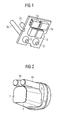
- FIG. 1 An essential component of a light signal is that shown in FIG 1, equipped with four LEDs 1a, 1b, 1c and 1d Board 2.
- the current supply of the LED 1a, 1b, 1c and 1d takes place via two connection wires 3a and 3b.
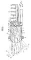
- the two upper LEDs 1a and 1b are light exit side with optical fibers 4a and 4b a illustrated in Figure 2 optics 5 connected.
- the both arranged approximately centrally on the board 2 LED 1c and 1d radiate their light on the upper part of a lens body 6 of the optics 5.
- the lower part of the lens body 6 is both light entry side and coat side with a Absorption surface 7 provided for sunlight.
- FIG. 3 shows the LED board 2 in the assembled state.
- the optics 5 is housed in a housing 8, which is close to the light exit surface the optic 5 in a matrix plate 9 sealing is pressed and rear locking elements for insertion the LED board 2 has.
- a housing 8 which is close to the light exit surface the optic 5 in a matrix plate 9 sealing is pressed and rear locking elements for insertion the LED board 2 has.
- LED modules 10 fully populated matrix plate 9, which is virtually the radiating surface of the light signal is shown in FIG. 4.
- the LED 1a. 1b. 1c, 1d with front lenses 11 are equipped for pre-focusing the LED light and that the LED board 2 for heat dissipation with a rib-shaped Heat sink 12 is connected.
- the light of the upper LED 1a and 1b, which is irradiated in the optical fibers 4a and 4b becomes thereby relatively wide, in particular down and to the side scattered, so that an optimal recognizability of the signal concept at close range.
- Some near-field rays are marked with 13.
- the lens body 6 beams 14 which are essentially of from the light of the LEDs 1c and 1d.
- Incident sunlight 15 is above a sun's position of 10 ° above the Horizon through the optics 5 completely on the absorption surface 7 directs that phantom light can not occur.
- the invention is not limited to the above Embodiment. Rather, it is a number of variants conceivable, which also with fundamentally different kind Execution of the features of the invention make use.
Landscapes
- Engineering & Computer Science (AREA)
- Mechanical Engineering (AREA)
- Non-Portable Lighting Devices Or Systems Thereof (AREA)
- Silicon Polymers (AREA)
- Cookers (AREA)
- Details Of Television Scanning (AREA)
- Illuminated Signs And Luminous Advertising (AREA)
- Traffic Control Systems (AREA)
- Led Device Packages (AREA)
- Gyroscopes (AREA)
- Audible And Visible Signals (AREA)
- Arrangement Of Elements, Cooling, Sealing, Or The Like Of Lighting Devices (AREA)
Abstract
Description
- Figur 1
- eine LED-Platine,
- Figur 2
- eine Optik mit Absorptionsfläche,
- Figur 3
- ein Optikgehäuse mit Matrixplatte und LED-Platine,
- Figur 4
- eine vollbestückte Matrixplatte und
- Figur 5
- einen Querschnitt durch ein LED-Modul mit Strahlengängen.
Claims (4)
- Lichtsignal mit einer Mehrzahl im Wesentlichen gleichartiger LED-Module (10), insbesondere zur Fernbereichs- und Nahbereichsdarstellung von Signalbegriffen bei schienengebundenen Verkehrswegen,
dadurch gekennzeichnet, dass jedes LED-Modul (10) mindestens eine Nahbereichs-LED (1a, 1b) und mindestens eine Fernbereichs-LED (1c, 1d) sowie eine das LED-Licht bündelnde Optik (5) aufweist, wobei die Nahbereichs-LED (1a, 1b) lichtaustrittsseitig mit einem zumindest teilweise in die Optik (5) integrierten Lichtleiter (4a, 4b) verbunden ist. - Lichtsignal nach Anspruch 1,
dadurch gekennzeichnet, dass jedes LED-Modul (10) zwei im Wesentlichen mittig zur Lichteintrittsfläche der Optik (5) angeordnete Fernbereichs-LED (1c, 1d) und zwei oberhalb derselben angeordnete Nahbereichs-LED (1a, 1b) aufweist, wobei die Optik (5) im unteren Bereich lichteintrittsseitig und mantelseitig eine Absorptionsfläche (7) für Sonnelicht aufweist. - Lichtsignal nach einem der vorangehenden Ansprüche,
dadurch gekennzeichnet, dass Optikgehäuse (8) vorgesehen sind, welche in einer vorgelochten Matrixplatte (9) dichtend eingedrückt und gegebenenfalls zusätzlich eingedübelt sind und an die lichteintrittsseitig LED-bestückte Platinen (2) angeschnappt sind. - Lichtsignal nach Anspruch 3,
dadurch gekennzeichnet, dass die Platinen (2) zur Wärmeableitung Durchkontaktierungen aufweisen, welche über Kupferflächen mit rippenförmigen Kühlkörpern (12) verbunden sind.
Priority Applications (2)
| Application Number | Priority Date | Filing Date | Title |
|---|---|---|---|
| SI200430340T SI1535820T1 (sl) | 2003-11-25 | 2004-11-12 | Svetlobni signal |
| PL04090430T PL1535820T3 (pl) | 2003-11-25 | 2004-11-12 | Sygnał świetlny |
Applications Claiming Priority (2)
| Application Number | Priority Date | Filing Date | Title |
|---|---|---|---|
| DE10355878A DE10355878B3 (de) | 2003-11-25 | 2003-11-25 | Lichtsignal |
| DE10355878 | 2003-11-25 |
Publications (3)
| Publication Number | Publication Date |
|---|---|
| EP1535820A2 true EP1535820A2 (de) | 2005-06-01 |
| EP1535820A3 EP1535820A3 (de) | 2006-06-07 |
| EP1535820B1 EP1535820B1 (de) | 2007-03-21 |
Family
ID=34442359
Family Applications (1)
| Application Number | Title | Priority Date | Filing Date |
|---|---|---|---|
| EP04090430A Expired - Lifetime EP1535820B1 (de) | 2003-11-25 | 2004-11-12 | Lichtsignal |
Country Status (8)
| Country | Link |
|---|---|
| EP (1) | EP1535820B1 (de) |
| AT (1) | ATE357362T1 (de) |
| DE (2) | DE10355878B3 (de) |
| DK (1) | DK1535820T3 (de) |
| ES (1) | ES2281751T3 (de) |
| PL (1) | PL1535820T3 (de) |
| PT (1) | PT1535820E (de) |
| SI (1) | SI1535820T1 (de) |
Cited By (2)
| Publication number | Priority date | Publication date | Assignee | Title |
|---|---|---|---|---|
| WO2011157597A1 (de) * | 2010-06-16 | 2011-12-22 | Siemens Aktiengesellschaft | Lichtsignal |
| EP3480078A1 (de) * | 2017-11-07 | 2019-05-08 | Siemens Schweiz AG | Lichtsignal zur anzeige von signalbegriffen für einen verkehrsweg |
Families Citing this family (1)
| Publication number | Priority date | Publication date | Assignee | Title |
|---|---|---|---|---|
| IT1396088B1 (it) † | 2009-10-16 | 2012-11-09 | Solari Di Udine S P A | Dispositivo di segnalazione luminosa a led e relativo procedimento di controllo |
Family Cites Families (6)
| Publication number | Priority date | Publication date | Assignee | Title |
|---|---|---|---|---|
| GB502980A (en) * | 1937-10-13 | 1939-03-29 | James Boot | Improvements in colour-light signals |
| DE930593C (de) * | 1949-07-29 | 1955-07-21 | Westinghouse Brake & Signal | Einrichtung zur Erzeugung eines Lichtbuendels |
| ATA174989A (de) * | 1989-07-20 | 1999-06-15 | Zelisko Josef Elektro Masch | Signalanordnung mit einem strahler |
| US5833355A (en) * | 1996-12-06 | 1998-11-10 | Dialight Corporation | Led illuminated lamp assembly |
| DE29706646U1 (de) * | 1997-04-14 | 1997-10-09 | Zentrum für Sonnenenergie- und Wasserstoff-Forschung Baden-Württemberg(ZSW), 70565 Stuttgart | Lichtquelle |
| DE19922361C2 (de) * | 1999-05-14 | 2003-05-28 | Osram Opto Semiconductors Gmbh | LED-Modul für Anzeigeeinrichtungen |
-
2003
- 2003-11-25 DE DE10355878A patent/DE10355878B3/de not_active Expired - Fee Related
-
2004
- 2004-11-12 ES ES04090430T patent/ES2281751T3/es not_active Expired - Lifetime
- 2004-11-12 PL PL04090430T patent/PL1535820T3/pl unknown
- 2004-11-12 EP EP04090430A patent/EP1535820B1/de not_active Expired - Lifetime
- 2004-11-12 DK DK04090430T patent/DK1535820T3/da active
- 2004-11-12 AT AT04090430T patent/ATE357362T1/de not_active IP Right Cessation
- 2004-11-12 DE DE502004003268T patent/DE502004003268D1/de not_active Expired - Lifetime
- 2004-11-12 PT PT04090430T patent/PT1535820E/pt unknown
- 2004-11-12 SI SI200430340T patent/SI1535820T1/sl unknown
Cited By (2)
| Publication number | Priority date | Publication date | Assignee | Title |
|---|---|---|---|---|
| WO2011157597A1 (de) * | 2010-06-16 | 2011-12-22 | Siemens Aktiengesellschaft | Lichtsignal |
| EP3480078A1 (de) * | 2017-11-07 | 2019-05-08 | Siemens Schweiz AG | Lichtsignal zur anzeige von signalbegriffen für einen verkehrsweg |
Also Published As
| Publication number | Publication date |
|---|---|
| PL1535820T3 (pl) | 2007-08-31 |
| DK1535820T3 (da) | 2007-07-30 |
| SI1535820T1 (sl) | 2007-08-31 |
| EP1535820A3 (de) | 2006-06-07 |
| PT1535820E (pt) | 2007-04-30 |
| ES2281751T3 (es) | 2007-10-01 |
| ATE357362T1 (de) | 2007-04-15 |
| DE502004003268D1 (de) | 2007-05-03 |
| DE10355878B3 (de) | 2005-08-25 |
| EP1535820B1 (de) | 2007-03-21 |
Similar Documents
| Publication | Publication Date | Title |
|---|---|---|
| EP3021041B1 (de) | Lichtquellenmodul für einen fahrzeugscheinwerfer | |
| EP1643188B1 (de) | Leuchtdiodenanordnung mit einer Kühlvorrichtung und Kfz-Scheinwerfer | |
| DE102010056313C5 (de) | Beleuchtungseinrichtung eines Kraftfahrzeugs | |
| DE69935547T2 (de) | Mit Vertiefungen versehner, optischer Verteiler für Fahrzeug-Beleuchtungssystem | |
| EP1805815B1 (de) | Beleuchtungseinrichtung, kfz-scheinwerfer und verfahren zur herstellung einer beleuctungseinrichtung | |
| EP2307792B1 (de) | Leuchte | |
| EP1327558A2 (de) | Fahrzeugleuchte | |
| DE202009011500U1 (de) | Optisches System für eine LED-Leuchte | |
| EP2816276A2 (de) | Kraftfahrzeug mit einer Leuchtvorrichtung | |
| AT512589B1 (de) | Lichtleitelement für einen Laser-Fahrzeugscheinwerfer sowie Fahrzeugscheinwerfer | |
| WO2019076550A1 (de) | Beleuchtungsvorrichtung für einen kraftfahrzeugscheinwerfer | |
| WO2013034395A1 (de) | Beleuchtungsvorrichtung | |
| DE202009014103U1 (de) | Leuchteinheit für eine Straßenlaterne | |
| DE102010013045A1 (de) | Fahrzeugleuchte mit einer Lichtleiter-Vorsatzoptik | |
| EP2494271B1 (de) | Leuchte zum ausleuchten eines zielbereiches mittels rückwärtsreflexion von licht eines leuchtdiodenmoduls an einem reflektor | |
| DE102008056049A1 (de) | Licht emittierende Vorrichtung umfassend mindestens eine Leuchtdiode und Beleuchtungseinrichtung für ein Kraftfahrzeug umfassend eine solche Vorrichtung | |
| DE20219483U1 (de) | Fahrzeugleuchte | |
| EP1431158A1 (de) | Signal- und Fahrlichtscheinwerfer für Schienenfahrzeuge | |
| DE10355878B3 (de) | Lichtsignal | |
| DE102020203735A1 (de) | Fahrzeug-Retrofit-Scheinwerferlampe mit einander zugewandten Reflektorbereichen | |
| DE102011051541A1 (de) | Beleuchtungsvorrichtung für Fahrzeuge | |
| DE20004188U1 (de) | Leuchte | |
| EP1913302B1 (de) | Leuchte für kraftfahrzeuge | |
| DE102014208504A1 (de) | Beleuchtungseinrichtung | |
| EP1362740B1 (de) | Fahrzeugleuchte |
Legal Events
| Date | Code | Title | Description |
|---|---|---|---|
| PUAI | Public reference made under article 153(3) epc to a published international application that has entered the european phase |
Free format text: ORIGINAL CODE: 0009012 |
|
| AK | Designated contracting states |
Kind code of ref document: A2 Designated state(s): AT BE BG CH CY CZ DE DK EE ES FI FR GB GR HU IE IS IT LI LU MC NL PL PT RO SE SI SK TR |
|
| AX | Request for extension of the european patent |
Extension state: AL HR LT LV MK YU |
|
| PUAL | Search report despatched |
Free format text: ORIGINAL CODE: 0009013 |
|
| AK | Designated contracting states |
Kind code of ref document: A3 Designated state(s): AT BE BG CH CY CZ DE DK EE ES FI FR GB GR HU IE IS IT LI LU MC NL PL PT RO SE SI SK TR |
|
| AX | Request for extension of the european patent |
Extension state: AL HR LT LV MK YU |
|
| 17P | Request for examination filed |
Effective date: 20060710 |
|
| GRAP | Despatch of communication of intention to grant a patent |
Free format text: ORIGINAL CODE: EPIDOSNIGR1 |
|
| GRAS | Grant fee paid |
Free format text: ORIGINAL CODE: EPIDOSNIGR3 |
|
| AKX | Designation fees paid |
Designated state(s): AT BE BG CH CY CZ DE DK EE ES FI FR GB GR HU IE IS IT LI LU MC NL PL PT RO SE SI SK TR |
|
| GRAA | (expected) grant |
Free format text: ORIGINAL CODE: 0009210 |
|
| AK | Designated contracting states |
Kind code of ref document: B1 Designated state(s): AT BE BG CH CY CZ DE DK EE ES FI FR GB GR HU IE IS IT LI LU MC NL PL PT RO SE SI SK TR |
|
| REG | Reference to a national code |
Ref country code: GB Ref legal event code: FG4D Free format text: NOT ENGLISH |
|
| REG | Reference to a national code |
Ref country code: RO Ref legal event code: EPE |
|
| REG | Reference to a national code |
Ref country code: CH Ref legal event code: EP |
|
| REG | Reference to a national code |
Ref country code: CH Ref legal event code: NV Representative=s name: SIEMENS SCHWEIZ AG Ref country code: PT Ref legal event code: SC4A Free format text: AVAILABILITY OF NATIONAL TRANSLATION Effective date: 20070416 |
|
| REF | Corresponds to: |
Ref document number: 502004003268 Country of ref document: DE Date of ref document: 20070503 Kind code of ref document: P |
|
| REG | Reference to a national code |
Ref country code: IE Ref legal event code: FG4D Free format text: LANGUAGE OF EP DOCUMENT: GERMAN |
|
| GBT | Gb: translation of ep patent filed (gb section 77(6)(a)/1977) |
Effective date: 20070523 |
|
| REG | Reference to a national code |
Ref country code: GR Ref legal event code: EP Ref document number: 20070401530 Country of ref document: GR |
|
| REG | Reference to a national code |
Ref country code: SE Ref legal event code: TRGR |
|
| PG25 | Lapsed in a contracting state [announced via postgrant information from national office to epo] |
Ref country code: IS Free format text: LAPSE BECAUSE OF FAILURE TO SUBMIT A TRANSLATION OF THE DESCRIPTION OR TO PAY THE FEE WITHIN THE PRESCRIBED TIME-LIMIT Effective date: 20070721 |
|
| REG | Reference to a national code |
Ref country code: DK Ref legal event code: T3 |
|
| ET | Fr: translation filed | ||
| REG | Reference to a national code |
Ref country code: PL Ref legal event code: T3 |
|
| REG | Reference to a national code |
Ref country code: ES Ref legal event code: FG2A Ref document number: 2281751 Country of ref document: ES Kind code of ref document: T3 |
|
| REG | Reference to a national code |
Ref country code: IE Ref legal event code: FD4D |
|
| PLBE | No opposition filed within time limit |
Free format text: ORIGINAL CODE: 0009261 |
|
| STAA | Information on the status of an ep patent application or granted ep patent |
Free format text: STATUS: NO OPPOSITION FILED WITHIN TIME LIMIT |
|
| PG25 | Lapsed in a contracting state [announced via postgrant information from national office to epo] |
Ref country code: IE Free format text: LAPSE BECAUSE OF FAILURE TO SUBMIT A TRANSLATION OF THE DESCRIPTION OR TO PAY THE FEE WITHIN THE PRESCRIBED TIME-LIMIT Effective date: 20070321 |
|
| 26N | No opposition filed |
Effective date: 20071227 |
|
| REG | Reference to a national code |
Ref country code: HU Ref legal event code: AG4A Ref document number: E002888 Country of ref document: HU |
|
| REG | Reference to a national code |
Ref country code: CH Ref legal event code: PCAR Free format text: SIEMENS SCHWEIZ AG;INTELLECTUAL PROPERTY FREILAGERSTRASSE 40;8047 ZUERICH (CH) |
|
| PGFP | Annual fee paid to national office [announced via postgrant information from national office to epo] |
Ref country code: CH Payment date: 20090205 Year of fee payment: 5 |
|
| PG25 | Lapsed in a contracting state [announced via postgrant information from national office to epo] |
Ref country code: CY Free format text: LAPSE BECAUSE OF FAILURE TO SUBMIT A TRANSLATION OF THE DESCRIPTION OR TO PAY THE FEE WITHIN THE PRESCRIBED TIME-LIMIT Effective date: 20070321 |
|
| PGFP | Annual fee paid to national office [announced via postgrant information from national office to epo] |
Ref country code: AT Payment date: 20091019 Year of fee payment: 6 Ref country code: CZ Payment date: 20091109 Year of fee payment: 6 Ref country code: DK Payment date: 20091110 Year of fee payment: 6 Ref country code: EE Payment date: 20091111 Year of fee payment: 6 Ref country code: ES Payment date: 20091207 Year of fee payment: 6 Ref country code: FI Payment date: 20091110 Year of fee payment: 6 Ref country code: LU Payment date: 20091113 Year of fee payment: 6 Ref country code: MC Payment date: 20091112 Year of fee payment: 6 Ref country code: SE Payment date: 20091110 Year of fee payment: 6 Ref country code: TR Payment date: 20091026 Year of fee payment: 6 |
|
| PGFP | Annual fee paid to national office [announced via postgrant information from national office to epo] |
Ref country code: NL Payment date: 20091118 Year of fee payment: 6 Ref country code: PL Payment date: 20091027 Year of fee payment: 6 Ref country code: SK Payment date: 20091109 Year of fee payment: 6 Ref country code: SI Payment date: 20091030 Year of fee payment: 6 |
|
| PGFP | Annual fee paid to national office [announced via postgrant information from national office to epo] |
Ref country code: PT Payment date: 20091026 Year of fee payment: 6 Ref country code: BG Payment date: 20091116 Year of fee payment: 6 |
|
| PGFP | Annual fee paid to national office [announced via postgrant information from national office to epo] |
Ref country code: FR Payment date: 20091203 Year of fee payment: 6 Ref country code: GB Payment date: 20091112 Year of fee payment: 6 Ref country code: HU Payment date: 20100122 Year of fee payment: 6 Ref country code: IT Payment date: 20091125 Year of fee payment: 6 Ref country code: RO Payment date: 20091103 Year of fee payment: 6 |
|
| PGFP | Annual fee paid to national office [announced via postgrant information from national office to epo] |
Ref country code: BE Payment date: 20091116 Year of fee payment: 6 Ref country code: DE Payment date: 20100118 Year of fee payment: 6 Ref country code: GR Payment date: 20091112 Year of fee payment: 6 |
|
| REG | Reference to a national code |
Ref country code: CH Ref legal event code: PL |
|
| PG25 | Lapsed in a contracting state [announced via postgrant information from national office to epo] |
Ref country code: LI Free format text: LAPSE BECAUSE OF NON-PAYMENT OF DUE FEES Effective date: 20091130 Ref country code: CH Free format text: LAPSE BECAUSE OF NON-PAYMENT OF DUE FEES Effective date: 20091130 |
|
| REG | Reference to a national code |
Ref country code: PT Ref legal event code: MM4A Free format text: LAPSE DUE TO NON-PAYMENT OF FEES Effective date: 20110512 |
|
| BERE | Be: lapsed |
Owner name: SIEMENS A.G. Effective date: 20101130 |
|
| REG | Reference to a national code |
Ref country code: NL Ref legal event code: V1 Effective date: 20110601 |
|
| REG | Reference to a national code |
Ref country code: SE Ref legal event code: EUG |
|
| PG25 | Lapsed in a contracting state [announced via postgrant information from national office to epo] |
Ref country code: MC Free format text: LAPSE BECAUSE OF NON-PAYMENT OF DUE FEES Effective date: 20101130 |
|
| REG | Reference to a national code |
Ref country code: DK Ref legal event code: EBP |
|
| GBPC | Gb: european patent ceased through non-payment of renewal fee |
Effective date: 20101112 |
|
| PG25 | Lapsed in a contracting state [announced via postgrant information from national office to epo] |
Ref country code: GR Free format text: LAPSE BECAUSE OF NON-PAYMENT OF DUE FEES Effective date: 20110602 Ref country code: EE Free format text: LAPSE BECAUSE OF NON-PAYMENT OF DUE FEES Effective date: 20101130 Ref country code: PT Free format text: LAPSE BECAUSE OF NON-PAYMENT OF DUE FEES Effective date: 20110512 Ref country code: HU Free format text: LAPSE BECAUSE OF NON-PAYMENT OF DUE FEES Effective date: 20101113 Ref country code: CZ Free format text: LAPSE BECAUSE OF NON-PAYMENT OF DUE FEES Effective date: 20101112 |
|
| REG | Reference to a national code |
Ref country code: SK Ref legal event code: MM4A Ref document number: E 1957 Country of ref document: SK Effective date: 20101112 |
|
| REG | Reference to a national code |
Ref country code: EE Ref legal event code: MM4A Ref document number: E001207 Country of ref document: EE Effective date: 20101130 |
|
| REG | Reference to a national code |
Ref country code: FR Ref legal event code: ST Effective date: 20110801 |
|
| PG25 | Lapsed in a contracting state [announced via postgrant information from national office to epo] |
Ref country code: FI Free format text: LAPSE BECAUSE OF NON-PAYMENT OF DUE FEES Effective date: 20101112 Ref country code: BG Free format text: LAPSE BECAUSE OF NON-PAYMENT OF DUE FEES Effective date: 20110630 Ref country code: AT Free format text: LAPSE BECAUSE OF NON-PAYMENT OF DUE FEES Effective date: 20101112 Ref country code: NL Free format text: LAPSE BECAUSE OF NON-PAYMENT OF DUE FEES Effective date: 20110601 Ref country code: SK Free format text: LAPSE BECAUSE OF NON-PAYMENT OF DUE FEES Effective date: 20101112 Ref country code: BE Free format text: LAPSE BECAUSE OF NON-PAYMENT OF DUE FEES Effective date: 20101130 |
|
| REG | Reference to a national code |
Ref country code: SI Ref legal event code: KO00 Effective date: 20110722 |
|
| REG | Reference to a national code |
Ref country code: DE Ref legal event code: R119 Ref document number: 502004003268 Country of ref document: DE Effective date: 20110601 Ref country code: DE Ref legal event code: R119 Ref document number: 502004003268 Country of ref document: DE Effective date: 20110531 |
|
| PG25 | Lapsed in a contracting state [announced via postgrant information from national office to epo] |
Ref country code: SE Free format text: LAPSE BECAUSE OF NON-PAYMENT OF DUE FEES Effective date: 20101113 |
|
| PG25 | Lapsed in a contracting state [announced via postgrant information from national office to epo] |
Ref country code: FR Free format text: LAPSE BECAUSE OF NON-PAYMENT OF DUE FEES Effective date: 20101130 Ref country code: DK Free format text: LAPSE BECAUSE OF NON-PAYMENT OF DUE FEES Effective date: 20101130 |
|
| PG25 | Lapsed in a contracting state [announced via postgrant information from national office to epo] |
Ref country code: RO Free format text: LAPSE BECAUSE OF NON-PAYMENT OF DUE FEES Effective date: 20101112 Ref country code: SI Free format text: LAPSE BECAUSE OF NON-PAYMENT OF DUE FEES Effective date: 20101113 Ref country code: GB Free format text: LAPSE BECAUSE OF NON-PAYMENT OF DUE FEES Effective date: 20101112 |
|
| PG25 | Lapsed in a contracting state [announced via postgrant information from national office to epo] |
Ref country code: IT Free format text: LAPSE BECAUSE OF NON-PAYMENT OF DUE FEES Effective date: 20101112 |
|
| REG | Reference to a national code |
Ref country code: PL Ref legal event code: LAPE |
|
| PG25 | Lapsed in a contracting state [announced via postgrant information from national office to epo] |
Ref country code: PL Free format text: LAPSE BECAUSE OF NON-PAYMENT OF DUE FEES Effective date: 20101112 |
|
| REG | Reference to a national code |
Ref country code: ES Ref legal event code: FD2A Effective date: 20120305 |
|
| PG25 | Lapsed in a contracting state [announced via postgrant information from national office to epo] |
Ref country code: ES Free format text: LAPSE BECAUSE OF NON-PAYMENT OF DUE FEES Effective date: 20101113 |
|
| PG25 | Lapsed in a contracting state [announced via postgrant information from national office to epo] |
Ref country code: LU Free format text: LAPSE BECAUSE OF NON-PAYMENT OF DUE FEES Effective date: 20101112 |
|
| PG25 | Lapsed in a contracting state [announced via postgrant information from national office to epo] |
Ref country code: TR Free format text: LAPSE BECAUSE OF NON-PAYMENT OF DUE FEES Effective date: 20101112 |
|
| PG25 | Lapsed in a contracting state [announced via postgrant information from national office to epo] |
Ref country code: DE Free format text: LAPSE BECAUSE OF NON-PAYMENT OF DUE FEES Effective date: 20110531 |