EP1536122B1 - Drive device for inductive electroactuators - Google Patents
Drive device for inductive electroactuators Download PDFInfo
- Publication number
- EP1536122B1 EP1536122B1 EP04106051A EP04106051A EP1536122B1 EP 1536122 B1 EP1536122 B1 EP 1536122B1 EP 04106051 A EP04106051 A EP 04106051A EP 04106051 A EP04106051 A EP 04106051A EP 1536122 B1 EP1536122 B1 EP 1536122B1
- Authority
- EP
- European Patent Office
- Prior art keywords
- control
- circuit
- drive device
- drive
- electrical
- Prior art date
- Legal status (The legal status is an assumption and is not a legal conclusion. Google has not performed a legal analysis and makes no representation as to the accuracy of the status listed.)
- Expired - Lifetime
Links
- 230000001939 inductive effect Effects 0.000 title claims abstract description 13
- 230000015654 memory Effects 0.000 claims abstract description 59
- 230000001105 regulatory effect Effects 0.000 claims abstract description 4
- 238000004891 communication Methods 0.000 claims description 10
- 230000001276 controlling effect Effects 0.000 claims description 7
- 238000005259 measurement Methods 0.000 claims description 4
- 230000004913 activation Effects 0.000 claims description 2
- 239000000446 fuel Substances 0.000 description 13
- 239000003990 capacitor Substances 0.000 description 12
- 238000002347 injection Methods 0.000 description 12
- 239000007924 injection Substances 0.000 description 12
- 230000006870 function Effects 0.000 description 9
- 230000009471 action Effects 0.000 description 3
- 230000005284 excitation Effects 0.000 description 3
- 230000001965 increasing effect Effects 0.000 description 3
- 230000000630 rising effect Effects 0.000 description 3
- 238000002485 combustion reaction Methods 0.000 description 2
- 239000004020 conductor Substances 0.000 description 2
- 238000010586 diagram Methods 0.000 description 2
- 231100001261 hazardous Toxicity 0.000 description 2
- VNWKTOKETHGBQD-UHFFFAOYSA-N methane Chemical compound C VNWKTOKETHGBQD-UHFFFAOYSA-N 0.000 description 2
- 238000012544 monitoring process Methods 0.000 description 2
- 238000011084 recovery Methods 0.000 description 2
- 238000012546 transfer Methods 0.000 description 2
- 238000013459 approach Methods 0.000 description 1
- 230000008859 change Effects 0.000 description 1
- 230000009977 dual effect Effects 0.000 description 1
- 238000009413 insulation Methods 0.000 description 1
- 239000000463 material Substances 0.000 description 1
- 238000012986 modification Methods 0.000 description 1
- 230000004048 modification Effects 0.000 description 1
- 230000008672 reprogramming Effects 0.000 description 1
- 230000000284 resting effect Effects 0.000 description 1
- 230000001360 synchronised effect Effects 0.000 description 1
- 230000007704 transition Effects 0.000 description 1
Images



Classifications
-
- F—MECHANICAL ENGINEERING; LIGHTING; HEATING; WEAPONS; BLASTING
- F02—COMBUSTION ENGINES; HOT-GAS OR COMBUSTION-PRODUCT ENGINE PLANTS
- F02D—CONTROLLING COMBUSTION ENGINES
- F02D41/00—Electrical control of supply of combustible mixture or its constituents
- F02D41/20—Output circuits, e.g. for controlling currents in command coils
-
- F—MECHANICAL ENGINEERING; LIGHTING; HEATING; WEAPONS; BLASTING
- F02—COMBUSTION ENGINES; HOT-GAS OR COMBUSTION-PRODUCT ENGINE PLANTS
- F02D—CONTROLLING COMBUSTION ENGINES
- F02D41/00—Electrical control of supply of combustible mixture or its constituents
- F02D41/24—Electrical control of supply of combustible mixture or its constituents characterised by the use of digital means
- F02D41/2406—Electrical control of supply of combustible mixture or its constituents characterised by the use of digital means using essentially read only memories
- F02D41/2425—Particular ways of programming the data
- F02D41/2487—Methods for rewriting
-
- F—MECHANICAL ENGINEERING; LIGHTING; HEATING; WEAPONS; BLASTING
- F02—COMBUSTION ENGINES; HOT-GAS OR COMBUSTION-PRODUCT ENGINE PLANTS
- F02D—CONTROLLING COMBUSTION ENGINES
- F02D41/00—Electrical control of supply of combustible mixture or its constituents
- F02D41/24—Electrical control of supply of combustible mixture or its constituents characterised by the use of digital means
- F02D41/26—Electrical control of supply of combustible mixture or its constituents characterised by the use of digital means using computer, e.g. microprocessor
- F02D41/266—Electrical control of supply of combustible mixture or its constituents characterised by the use of digital means using computer, e.g. microprocessor the computer being backed-up or assisted by another circuit, e.g. analogue
-
- F—MECHANICAL ENGINEERING; LIGHTING; HEATING; WEAPONS; BLASTING
- F02—COMBUSTION ENGINES; HOT-GAS OR COMBUSTION-PRODUCT ENGINE PLANTS
- F02D—CONTROLLING COMBUSTION ENGINES
- F02D41/00—Electrical control of supply of combustible mixture or its constituents
- F02D41/20—Output circuits, e.g. for controlling currents in command coils
- F02D2041/2003—Output circuits, e.g. for controlling currents in command coils using means for creating a boost voltage, i.e. generation or use of a voltage higher than the battery voltage, e.g. to speed up injector opening
- F02D2041/2006—Output circuits, e.g. for controlling currents in command coils using means for creating a boost voltage, i.e. generation or use of a voltage higher than the battery voltage, e.g. to speed up injector opening by using a boost capacitor
-
- F—MECHANICAL ENGINEERING; LIGHTING; HEATING; WEAPONS; BLASTING
- F02—COMBUSTION ENGINES; HOT-GAS OR COMBUSTION-PRODUCT ENGINE PLANTS
- F02D—CONTROLLING COMBUSTION ENGINES
- F02D41/00—Electrical control of supply of combustible mixture or its constituents
- F02D41/20—Output circuits, e.g. for controlling currents in command coils
- F02D2041/202—Output circuits, e.g. for controlling currents in command coils characterised by the control of the circuit
- F02D2041/2058—Output circuits, e.g. for controlling currents in command coils characterised by the control of the circuit using information of the actual current value
-
- F—MECHANICAL ENGINEERING; LIGHTING; HEATING; WEAPONS; BLASTING
- F02—COMBUSTION ENGINES; HOT-GAS OR COMBUSTION-PRODUCT ENGINE PLANTS
- F02D—CONTROLLING COMBUSTION ENGINES
- F02D41/00—Electrical control of supply of combustible mixture or its constituents
- F02D41/20—Output circuits, e.g. for controlling currents in command coils
- F02D2041/2068—Output circuits, e.g. for controlling currents in command coils characterised by the circuit design or special circuit elements
- F02D2041/2072—Bridge circuits, i.e. the load being placed in the diagonal of a bridge to be controlled in both directions
-
- H—ELECTRICITY
- H01—ELECTRIC ELEMENTS
- H01H—ELECTRIC SWITCHES; RELAYS; SELECTORS; EMERGENCY PROTECTIVE DEVICES
- H01H47/00—Circuit arrangements not adapted to a particular application of the relay and designed to obtain desired operating characteristics or to provide energising current
- H01H47/22—Circuit arrangements not adapted to a particular application of the relay and designed to obtain desired operating characteristics or to provide energising current for supplying energising current for relay coil
- H01H47/32—Energising current supplied by semiconductor device
- H01H47/325—Energising current supplied by semiconductor device by switching regulator
Definitions
- the present invention relates to a drive device for inductive electroactuators.
- the present invention is advantageously, but not exclusively, used for driving electrical injectors of a fuel injection system for a motor vehicle internal combustion engine, in particular for a common rail fuel injection system for a diesel engine, to which the following explanation will make explicit reference, without consequently restricting the general scope thereof.
- the drive device according to the invention may nevertheless be used for other kinds of engines, such as petrol, methane or LPG engines, or for any other kind of inductive electroactuators, such as for example solenoid valves for ABS systems and the like, solenoid valves for variable timing systems, etc..
- engines such as petrol, methane or LPG engines
- inductive electroactuators such as for example solenoid valves for ABS systems and the like, solenoid valves for variable timing systems, etc.
- an electrical injector comprises an external body defining a cavity which communicates with the outside through an injection jet and in which there is accommodated an axially mobile pin to open and close the jet under the opposing axial thrusts of the pressure of the injected fuel, on the one hand, and of a spring and a rod, on the other, said rod being arranged along the axis of the plunger on the opposite side of the jet and being actuated by an electromagnetically driven metering valve.
- the electromagnet excitation current in the initial phase is rather high (first holding value).
- the rapid rise in the current profile to the first holding value is necessary to ensure sufficient timing accuracy with regard to the moment of onset of actuation.
- Said excitation current profile has in the past been obtained by using a drive device in which the electrical injectors were connected, on the one hand, directly to a supply line and, on the other, to a ground line through a controlled electronic switch.
- said drive device exhibited the disadvantage that any short circuit to ground of one of the terminals of any of the electrical injectors, for example due to a loss of insulation on a cable conductor of the said electrical injectors and contact of said conductor with the motor vehicle's bodywork, resulted in permanent damage to the electrical injector itself and/or to the drive device, so causing the motor vehicle to shut down, which is highly hazardous when it is in motion.
- the elevated voltage necessary to bring about the rapid rise in current in the initial opening phase of the electrical injector is generated by means of a boost circuit which is capable of raising the voltage supplied by the motor vehicle battery and essentially consists of a DC-DC converter.
- the DC-DC converter is dimensioned in accordance with the power which can be supplied to the electrical injector and, in particular, that the dimensions of the DC-DC converter increase as a function of the power it is desired to obtain from the output of the said DC-DC converter
- raising the fuel injection pressure would entail the use of a DC-DC converter of considerably larger dimensions than that presently used, with a consequent increase in the area occupied by the DC-DC converter, the overall bulk of the drive device and the associated costs.
- a voltage boost circuit which is made up of a single capacitor, the circuit being capable of recharging said capacitor using one or more electrical injectors which are non-operational, i.e. not involved in a fuel injection operation.
- an electrical injector is first of all identified which at that moment is not involved in a fuel injection operation, electrical energy is then stored in said electrical injector and finally the stored electrical energy is transferred from the electrical injector to the capacitor of the voltage boost circuit.
- the storage of electrical energy in one of the electrical injectors not involved in a fuel injection operation and the transfer of said stored energy to the capacitor of the voltage boost circuit are achieved by using the drive device shown in the example of Figure 1 , said device comprising a power circuit, designated 10 overall, which in turn comprises a plurality of drive circuits 11, one for each electrical injector 12; and a control circuit (not shown) capable of controlling the operation of each drive circuit 11.
- Figure 1 shows two drive circuits 11 associated with two respective electrical injectors 12 belonging to the same cylinder bank of the engine (not shown), each of which injectors is shown in the Figure with its corresponding equivalent circuit made up of a resistor and an inductor connected in series.
- Each drive circuit 11 comprises a first and a second input terminal 13, 14, connected to the positive pole and the negative pole of the motor vehicle's battery 23, said battery supplying a voltage V BATT , the nominal value of which is typically 12 V; a third and a fourth input terminal 15, 16, connected to a first and a second output terminal of a boost circuit 8 which is common to all the drive circuits 11, between which it supplies a boosted voltage V BOOST greater than the battery voltage V BATT , for example 50 V; and a first and a second output terminal 19, 20, between which is connected the associated electrical injector 12.
- each electrical injector 12 connected to the first output terminal 19 of the associated drive circuit 11 is typically known as the "high” or “hot” side terminal, while the terminal of each electrical injector 12 connected to the second output terminal 20 of the associated drive circuit 11 is typically known as the "low” or “cold” side terminal.
- the boost circuit 8 is made up of a single, "boost" capacitor 21, connected between the first and the second output terminal of the boost circuit 8, and across which is connected a comparator stage with hysteresis 22 which outputs a logic signal which assumes a first logic level, for example high, when the voltage across the capacitor 21 is greater than a predetermined upper value, for example 50 V, and a second logic level, for example low, when the voltage across the capacitor 21 is less than a predetermined lower value, for example 49 V.
- a predetermined upper value for example 50 V
- a second logic level for example low
- Each drive circuit 11 moreover comprises a ground line 24 connected to the second input terminal 14 and to the fourth input terminal 16, and a supply line 25 connected, on the one hand, to the first input terminal 13 through a first diode 26, the anode of which is connected to the first input terminal 13 and the cathode of which is connected to the supply line 25, and, on the other, to the third input terminal 15 through a first MOS transistor 27, which has the gate terminal capable of receiving a first control signal from the control circuit (not shown), a well terminal connected to the third input terminal 15, and the source terminal connected to the supply line 25.
- Each drive circuit 11 moreover comprises a second MOS transistor 28 having a gate terminal receiving a second control signal supplied by the control circuit (not shown), a well terminal connected to the supply line 25, and a source terminal connected to the first output terminal 19; and a third MOS transistor 29 having a gate terminal receiving a third control signal supplied by the control circuit (not shown), a well terminal connected to the second output terminal 20, and a source terminal connected to the ground line 24 through a sensing stage made up of a sense resistor 31 across which there is connected an operational amplifier 32 generating an output voltage V s proportional to the current flowing in said sense resistor 31.
- Each drive circuit 11 moreover comprises a second, "free-wheeling" diode 33 with the anode connected to the ground line 24 and the cathode connected to the first output terminal 19; and a third, “boost” diode 34 with the anode connected to the second output terminal 20 and the cathode connected to the third input terminal 15.
- each drive circuit 11 may be subdivided into three main distinct phases characterised by a different profile of the current flowing in the electrical injector 12: a first, rapid charging or "boost" phase, in which the current rises rapidly up to a holding value capable of opening the electrical injector 12; a second, holding phase, in which the current oscillates with a sawtooth profile around the value reached in the preceding phase; and a third, rapid discharge phase, in which the current falls rapidly from the value assumed in the preceding phase to a final value, which may also be zero.
- a first, rapid charging or "boost" phase in which the current rises rapidly up to a holding value capable of opening the electrical injector 12
- a second, holding phase in which the current oscillates with a sawtooth profile around the value reached in the preceding phase
- a third, rapid discharge phase in which the current falls rapidly from the value assumed in the preceding phase to a final value, which may also be zero.
- the control circuit causes the transistors 27, 28 and 29 to close and the boosted voltage V BOOST is thus applied across the electrical injector 12.
- V BOOST the boosted voltage
- the current flows in the network comprising the capacitor 21, the transistor 27, the transistor 28, the electrical injector 12, the transistor 29 and the sense resistor 31, rising over time in substantially linear manner with a gradient equal to V BOOST /L (where L represents the equivalent series inductance of the electrical injector 12). Since V BOOST is much higher than V BATT , the current rises much more rapidly than could be achieved with V BATT .
- transistor 29 is closed, transistor 27 is open and transistor 28 is repeatedly closed and opened and the battery voltage V BATT (when transistor 28 is closed) and a zero voltage (when transistor 28 is open) are thus applied alternately across the electrical injector 12.
- the first case transistor 28 closed
- the second case transistor 28 open
- the control circuit causes the transistors 27, 28 and 29 to open, while current is passing through the electrical injector 12, the boosted voltage -V BOOST being applied across the electrical injector 12.
- current flows in the network comprising the capacitor 21, the boost diode 34, the electrical injector 12 and the free-wheeling diode 33, falling over time in substantially linear manner with a gradient equal to -V BOOST /L. Since V BOOST is much higher than V BATT , the current falls much more rapidly than could be achieved with V BATT .
- the percentage energy recovery associated with said phase may be at most around 25% (depending on the type of electrical injector, the materials used and the mechanical work performed by the electromagnet to move the rod).
- control signals for the above-stated transistors 27, 28 and 29 are generated by the control circuit on the basis of operating parameters stored in a memory integral with the said control device.
- EP 943 909 A1 An example with one control module for each drive circuit is shown in EP 943 909 A1 .
- control signals would be generated on the basis of non-homogeneous operating parameters, i.e. which do not relate to a single set of engine operating conditions, and this may result in the electroactuators being actuated in a manner which is inappropriate for current engine operating conditions.
- the object of the present invention is thus to provide a drive device for inductive electrical injectors which overcomes the above-described disadvantages.
- the present invention provides a drive device for inductive electroactuators equipped with a power circuit comprising a drive circuit for each electroactuator; each drive circuit comprising selectively controlled switching means for regulating the current flowing through said electroactuator; said drive device moreover comprising a control circuit which is capable of driving the operation of each control circuit of said power circuit and being characterised in that said control circuit comprises:
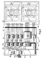
- 41 denotes the overall drive device for inductive electroactuators, which essentially comprises a power circuit 42 capable of supplying current to the electroactuators and a control circuit 43 capable of driving the power circuit 42 to regulate the current flowing through each electroactuator, in such a manner that, on the one hand, the current follows a predetermined profile over time, and on the other, the stored energy is transferred from an electrical injector to the capacitor of the voltage boost circuit (in accordance with the energy transfer criterion described above).
- the present invention is advantageously, but not exclusively, used for driving electrical injectors of a fuel injection system for a motor vehicle internal combustion engine, in particular for a common rail fuel injection system for a diesel engine, to which the following explanation will make explicit reference, without consequently restricting the general scope thereof.
- the power circuit 42 shown schematically in the example of Figure 2 is capable of controlling current in four electrical injectors 12 and comprises two power blocks 42a, 42b, each of which is made up of a circuit which is entirely similar to the power circuit 10 for controlling the two electrical injectors shown in Figure 1 , and consequently any elements in common with the power circuit 10 (of Figure 1 ) have been assigned the same reference numerals and will accordingly not be described in further detail.
- ASIC Application Specific Integrated Circuit
- the control circuit 43 essentially comprises: four control blocks 44 (only one of which is shown with a dashed line), one for each electrical injector (i.e. one for each drive circuit 11), a synchronisation block 45, a boost drive block 46, a current measurement block 47, and a communication block 48 capable of interfacing the control board or circuit 43 with one or more external control devices, in particular an external microcontroller 80.
- control bus 49 the various electrical blocks 43, 44, 45, 46, 47 and 48 stated above which make up the control circuit 43 are interconnected by means of a control bus 49, this bus being the means not only for exchanging control signals between the blocks themselves but also for exchanging control signals between said blocks and the external control devices, in particular with the external microcontroller 80.
- the measurement block 47 has the function of detecting, for each electrical injector 12, the voltage V s supplied by the corresponding sensing stage of the control circuit 11, of converting the analogue voltage signal V s into the digital signal S SENSE indicating the current flowing in the corresponding sense resistor 31, and, finally, of supplying the latter to a respective control block 44, whereas the communication block 48 manages the communication of control information, data or signals between the various blocks contained in the control circuit 43 and the external microcontroller 80.
- the communication block 48 is made up of a 16-bit communication interface (SPI interface) capable of effecting preferably synchronous communication and comprising a first control module (not shown) capable of managing the communication requests relating to data read/write operations made by the external microcontroller 80 or by the internal blocks; and a second control module (not shown) having the function of implementing a communication protocol capable of managing the addressing of data in the various memories and/or internal registers to the various blocks of the control circuit 43, in the various read/write operations.
- SPI interface 16-bit communication interface
- the boost drive block 46 has the function of controlling each first MOS transistor 27 of the drive device 41 for controlling the activation of the associated boost device.
- the boost drive circuit 46 is capable of managing the control of a pair of boost devices, each connected to two drive circuits 11, and is connected on the input side to the control bus 49 in order to receive a series of items of information, on the basis of which it generates the control signals of the first MOS transistors 27 of the boost devices.
- the synchronisation block 45 is connected to the control bus 49, from which it receives status signals S FLAG encoding information associated with the operating status of the control blocks 44, and outputs to the said control bus 49 a synchronisation signal S SINC capable of coordinating the drive actions issued by the control blocks 44 to the respective drive circuits 11.
- the control blocks 44 are capable of driving the operation of the respective drive circuits 11 and they check the instantaneous operating status of the corresponding electrical injectors 12.
- each control block 44 is capable of receiving the input signal S SENSE which indicates the value of the current flowing in the sense resistor 31 of the respective drive circuit 11; a feedback signal hs_fbk containing a series of items of information relating to the operating status of the second MOS transistor 28 (controlled switch 28 present on the "high side” of the drive circuit 11); and a feedback signal ls_ fbk containing a series of items of information relating to the operating status of the third MOS transistor 29 (controlled switch 29 present on the "low side” of the drive circuit 11).
- each control block 44 is moreover connected to the control bus 49 in order to receive from the latter a signal S SINC encoding a series of items of information capable of permitting the control block 44 itself to synchronise the commands to be issued to the drive circuit 11 with those issued by the other control blocks 44, in accordance with a predetermined common strategy for driving the electrical injectors 12.
- Each control block 44 is moreover capable of outputting a control signal hs_cmd to the second MOS transistor 28, a control signal ls_ cmd to the third MOS transistor 29, and a status signal S FLAG , which contains a series of items of information relating to the operating status of said control block 44, and is capable of being transmitted though the respective control bus 49 to the synchronisation block 45.
- the control block 44 encodes in the status signal S FLAG a plurality of control flags stored in some internal registers (not shown).
- each control block 44 comprises a pair of control stages, the first of which, hereinafter designated 44a, takes the form of an analogue circuit connected directly to a corresponding control circuit 11, while the second control stage, hereinafter designated 44b, is connected, on the one hand, to the control bus 49, and, on the other, to the first control stage 44a, to which it supplies the control signal hs_cmd from the second MOS transistor 28 and the control signal ls_cmd from the third MOS transistor 29.
- the first control stage 44a is provided with a series of output pins or terminals connected to the terminals of the second and third MOS transistor 28 and 29 in order to supply thereto polarisation voltages generated as a function of the control signals hs_cmd and ls_cmd.
- a first, second and third pin designated by the abbreviations DHS, GHS and SHS are respectively connected to the well, gate and source terminals of the second MOS transistor 29, while the fourth and fifth pin, respectively designated with the abbreviations DLS, GLS, are connected to the corresponding well and gate terminals of the second MOS transistor 29.
- the first control stage 44a is moreover provided with a circuit for monitoring the "high side” and a circuit for monitoring the "low side” (not shown), said circuits being capable of inputting into the second control stage 44b the respective feedback signals hs_fbk and ls_ fbk encoding the information relating to the operation of the second and third MOS transistors 28 and 29.
- the second control stage 44b is capable of receiving as input the feedback signals hs_fbk and ls_fbk from the first control stage 44a, and the synchronisation signal S SINC , and outputs the status signal S FLAG and the control signals hs_cmd and ls_cmd.
- the second control stage 44b is moreover capable of supplying, as a function of the feedback signals hs_fbk and ls_ fbk, the interrupt request signal to the external microcontroller 80, and a signal encoding a series of data generated by a request transmitted from the external microcontroller 80, and a signal S DAC which sets threshold levels for current quantisation in the comparators of the analogue circuit 47a.
- Figure 3 shows an example of the circuit architecture of the second control stage 44b, which essentially comprises a diagnostic block 60, a first counter block 61, an internal microcontroller 62, and a main memory 63.
- the diagnostic block 60 is capable of carrying out an instantaneous comparison between the output control signals hs_cmd and ls_cmd and the input feedback signals hs_fbk and ls_fbk, in such a manner as to detect any error conditions and then generate, as a function of said error conditions, the interrupt request signal to the internal microcontroller 62 and/or to the external microcontroller 80.
- the main memory 63 is capable of storing the program code containing the various instructions to be implemented in the internal microcontroller 62, and is made up of a RAM memory block (256x16) which cooperates with the first counter block 61 which stores the address relating to the instruction to be output to the internal microcontroller 62.
- the second control stage 44b moreover comprises a secondary memory 64 having two memory areas in which are stored the same operating parameters which characterise the operation of the electrical injector 12, and a series of pointer registers 71 which cooperate with the internal microcontroller 62 and with the external microcontroller 80 in order to define access of the internal microcontroller 62 to one memory area and, simultaneously, to define access of the external microcontroller 80 to the other memory area.
- the pointer registers 71 are moreover capable of cooperating with the internal microcontroller 62 and with the external microcontroller 80 to swap access rights to the two memory areas between the internal microcontroller 62 and the external microcontroller 80.
- read/write access operations of the secondary memory 64 are organised in such a manner that, when the internal microcontroller 62 accesses one of the two memory areas to read the operating parameters to be used in the ongoing control operations of the electrical injector 12, the external microcontroller 80 can only access the other memory area to carry out write operations (reprogramming or updating) on the operating parameters which will have to be used by the internal microcontroller 62 in the control operations of electrical injector 12 subsequent to the ongoing operations.
- the pointer registers 71 will alternately address the memory area accessible to the external microcontroller 80 and the memory area accessible to the internal microcontroller 62.
- Figures 4 and 5 illustrate schematically the subdivision and organisation of the secondary memory 64 in the two memory areas in two consecutive operating phases, in which in the first operating phase ( Figure 4 ) the pointer registers 71 address a first memory area 64a (highlighted in grey) to the external microcontroller 80, and an internal microcontroller 62 to a second memory area 64b.
- the first memory area 64a is thus only write-accessible to the external microcontroller 80 which overwrites or reprograms the operating parameters
- the second memory area 46b (not highlighted) is only read-accessible to the internal microcontroller 62, which accesses the operating parameters stored in said secondary memory area in order to generate control signals hs_cmd and ls_cmd as a function of said operating parameters.
- the transition from the first operating phase to the second operating phase takes place when the control block 44 receives a signal S START which indicates the onset of a new actuation of the electrical injector 12 and when the external microcontroller 80 has finished updating the control operating parameters in the first memory area 64a.
- first and second memory areas 64a and 64b are swapped, after which the first memory area 64a (not highlighted) becomes exclusively accessible to the internal microcontroller 62 which uses the previously modified operating parameters to control the new ongoing operations, while the second memory area 64b becomes exclusively accessible to the external microcontroller 80 which reprograms the operating parameters contained therein.
- the above-stated swapping of access rights to the two memory areas of the secondary memory 64 eliminates any data write/read conflict conditions between the internal microcontroller 62 and the external microcontroller 80 and advantageously makes it possible to implement a double buffer configuration in which the external microcontroller 80 can program the "new" operating parameters for the subsequent actuation control operations, while the "old” operating parameters remain unchanged, stable and available to the internal microcontroller 62 throughout the ongoing actuation control operations.
- the addresses associated to the first and second memory areas are temporarily stored in the respective pointer registers 71, the first pointer register (not shown) being capable of supplying to the internal microcontroller 62 the address of one of the two memory areas alternately assigned as read only, while a second register is capable of alternately supplying to the external microcontroller 80 the address of the other write-assigned memory area.
- the secondary memory 64 is preferably made up of a (32x16) DPRAM (Dual Port RAM) module comprising two memory blocks, each of which is capable of storing 16 words, and is connected to an address bus made up of 5 address lines in which four bits are used to address the words and a fifth bit is used to define access to the two memory blocks by the internal microcontroller 44b and the external microcontroller 80.
- DPRAM Dynamic RAM
- the second control stage 44b moreover comprises a series of first registers 70 used during data writing/reading in the second memory 64; a multiplexer block (not shown) capable of selecting the data to be stored in the first registers 70; and a second, preferably 8-bit, register (not shown) for storing the current quantisation thresholds of the measurement block 47.
- the second control stage 44b moreover comprises an auxiliary register 72 used as an auxiliary storage element during the management of the encoded instructions in the main memory 63, for example during execution of conditional or direct jump instructions.
- the internal microcontroller 62 has the function of receiving the instructions from the main memory 63, decoding them and executing them in such a manner as to generate the control signals hs_cmd and ls_cmd.
- the internal microcontroller 62 receives as input the actuation start command signal S START for the electrical injector, the feedback signals hs_fbk and ls_fbk, outputs the control signals hs_cmd and ls_cmd and is connected to the control bus 49 to exchange the control signals.
- the drive device 41 for electrical injectors is extremely advantageous in that the alternation of access rights by the external and internal microcontrollers to the operating parameters contained in the two memory areas of the secondary memory 64 ensures that the commands supplied to the electrical injectors are correctly generated, the commands being based on a set of operating parameters which are homogeneous, i.e. updated in accordance with the true operating conditions of the electroactuators themselves.
Landscapes
- Engineering & Computer Science (AREA)
- General Engineering & Computer Science (AREA)
- Chemical & Material Sciences (AREA)
- Combustion & Propulsion (AREA)
- Mechanical Engineering (AREA)
- Computer Hardware Design (AREA)
- Microelectronics & Electronic Packaging (AREA)
- Electrical Control Of Air Or Fuel Supplied To Internal-Combustion Engine (AREA)
- Fuel-Injection Apparatus (AREA)
- Electronic Switches (AREA)
- Control Of Electrical Variables (AREA)
- Control Of Electric Motors In General (AREA)
- Valve Device For Special Equipments (AREA)
- Control Of Stepping Motors (AREA)
Applications Claiming Priority (2)
| Application Number | Priority Date | Filing Date | Title |
|---|---|---|---|
| ITTO20030938 | 2003-11-25 | ||
| IT000938A ITTO20030938A1 (it) | 2003-11-25 | 2003-11-25 | Dispositivo di comando di elettroattuatori induttivi. |
Publications (3)
| Publication Number | Publication Date |
|---|---|
| EP1536122A2 EP1536122A2 (en) | 2005-06-01 |
| EP1536122A3 EP1536122A3 (en) | 2005-12-28 |
| EP1536122B1 true EP1536122B1 (en) | 2008-05-14 |
Family
ID=34452291
Family Applications (1)
| Application Number | Title | Priority Date | Filing Date |
|---|---|---|---|
| EP04106051A Expired - Lifetime EP1536122B1 (en) | 2003-11-25 | 2004-11-24 | Drive device for inductive electroactuators |
Country Status (6)
| Country | Link |
|---|---|
| US (1) | US7035728B2 (it) |
| EP (1) | EP1536122B1 (it) |
| JP (1) | JP4414324B2 (it) |
| AT (1) | ATE395507T1 (it) |
| DE (1) | DE602004013706D1 (it) |
| IT (1) | ITTO20030938A1 (it) |
Families Citing this family (8)
| Publication number | Priority date | Publication date | Assignee | Title |
|---|---|---|---|---|
| US7054737B2 (en) * | 2004-03-18 | 2006-05-30 | Ford Global Technologies, Llc | Power electronics circuit with voltage regulator for electromechanical valve actuator of an internal combustion engine |
| US7464689B2 (en) * | 2005-10-12 | 2008-12-16 | Gm Global Technology Operations, Inc. | Method and apparatus for controlling fuel injection into an engine |
| KR100967026B1 (ko) * | 2009-01-21 | 2010-06-30 | 주식회사 하이닉스반도체 | 불휘발성 메모리 장치 및 그 캐쉬리드 방법 |
| DK2633539T3 (en) * | 2010-10-25 | 2017-09-18 | Xio Inc | Method and apparatus for configurable actuation of a solenoid |
| US9291077B2 (en) * | 2012-04-27 | 2016-03-22 | Schaeffler Technologies AG & Co. KG | Operation control system for a solenoid valve of a combustion engine and method |
| FR3036222B1 (fr) | 2015-05-13 | 2017-04-28 | Stmicroelectronics Rousset | Procede de commande d'un changement d'etat de fonctionnement d'un organe electromecanique, par exemple un relais, et dispositif correspondant |
| US10087872B2 (en) | 2015-11-18 | 2018-10-02 | Infineon Technologies Ag | System and method for a synchronized driver circuit |
| US10221800B1 (en) * | 2018-01-22 | 2019-03-05 | Delphi Technologies Ip Limited | Fuel injector control including adaptive response |
Family Cites Families (7)
| Publication number | Priority date | Publication date | Assignee | Title |
|---|---|---|---|---|
| IT1195387B (it) * | 1983-02-22 | 1988-10-19 | Gianni Marani | Sequenziatore elettronico programmato e programmabile da utente direttamente dal pannello di comando della relativa apparecchiatura di servizio |
| DE3515040A1 (de) * | 1985-04-25 | 1986-07-24 | Klöckner, Wolfgang, Dr., 8033 Krailling | Verfahren und anordnung zur steuerung einer brennkraftmaschine |
| US5162998A (en) * | 1988-12-12 | 1992-11-10 | Matsushita Electric Industrial Co., Ltd. | Constant-speed regulating device for a vehicle |
| IT1296664B1 (it) * | 1997-12-19 | 1999-07-14 | Fiat Ricerche | Dispositivo di comando di elettroattuatori. |
| FR2776413B1 (fr) * | 1998-03-17 | 2000-05-26 | Renault | Systeme de generation de commandes d'actionneurs |
| US6735514B2 (en) * | 2000-10-16 | 2004-05-11 | Stmicroelectronics S.R.L. | Control device for a vehicle engine |
| JP2002357149A (ja) * | 2001-05-31 | 2002-12-13 | Aisan Ind Co Ltd | 電磁式燃料噴射弁の駆動回路 |
-
2003
- 2003-11-25 IT IT000938A patent/ITTO20030938A1/it unknown
-
2004
- 2004-11-17 US US10/989,725 patent/US7035728B2/en not_active Expired - Lifetime
- 2004-11-24 DE DE602004013706T patent/DE602004013706D1/de not_active Expired - Lifetime
- 2004-11-24 AT AT04106051T patent/ATE395507T1/de not_active IP Right Cessation
- 2004-11-24 EP EP04106051A patent/EP1536122B1/en not_active Expired - Lifetime
- 2004-11-25 JP JP2004340925A patent/JP4414324B2/ja not_active Expired - Fee Related
Also Published As
| Publication number | Publication date |
|---|---|
| EP1536122A3 (en) | 2005-12-28 |
| EP1536122A2 (en) | 2005-06-01 |
| DE602004013706D1 (de) | 2008-06-26 |
| JP4414324B2 (ja) | 2010-02-10 |
| US20050146805A1 (en) | 2005-07-07 |
| JP2005158080A (ja) | 2005-06-16 |
| ITTO20030938A1 (it) | 2005-05-26 |
| US7035728B2 (en) | 2006-04-25 |
| ATE395507T1 (de) | 2008-05-15 |
Similar Documents
| Publication | Publication Date | Title |
|---|---|---|
| JP2010174893A (ja) | 誘導型電気アクチュエータ用の動作装置 | |
| EP1536124B1 (en) | Drive device for electrical injectors of an internal combustion engine common rail fuel injection system | |
| GB2364576A (en) | A fuel injection conflict monitoring and resolution installation | |
| KR100284521B1 (ko) | 한 개 이상의 전자적 부하 제어장치 | |
| EP1536122B1 (en) | Drive device for inductive electroactuators | |
| JPH08512436A (ja) | 電磁的負荷を制御する装置及び方法 | |
| JP2000054932A (ja) | 少なくとも1つの磁石弁の制御方法及び装置 | |
| US5936827A (en) | Device for controlling at least one electromagnetic load | |
| WO1991017351A1 (en) | An apparatus for driving a piezoelectric actuator | |
| US7856964B2 (en) | Method of controlling a piezoelectric actuator | |
| JP2008514020A (ja) | 少なくとも1つの容量性負荷を充電および放電するための回路装置および方法 | |
| US6526945B2 (en) | Control circuit for controlling at least one solenoid valve for fuel metering in an internal combustion engine | |
| US5986360A (en) | Device and method for controlling at least one capacitive actuator | |
| US5907466A (en) | Device and process for activating at least two electromagnetic loads | |
| JP2001053348A (ja) | 複数の圧電素子を充電および放電するための装置 | |
| US20040196092A1 (en) | Electromagnetic load drive apparatus | |
| US20050231170A1 (en) | Circuit configuration for charging and discharging a plurality of capacitive actuators | |
| JP2021113538A (ja) | 電磁弁駆動装置 | |
| KR100886523B1 (ko) | 시스템 파라미터를 제어하기 위한 방법 및 장치 | |
| JP2018084198A (ja) | 電子制御装置 | |
| WO2005014992A1 (en) | Method for operating an inductive electroactuator control device | |
| US6943480B2 (en) | System for controlling a piezoelectric actuator, in particular for the fuel injectors of a diesel engine | |
| EP1860307B1 (en) | Method of controlling a piezoelectric actuator | |
| JPH11224816A (ja) | 電磁的負荷の制御方法および制御装置 | |
| CN104411956A (zh) | 用于操控至少一个燃料喷射阀的控制设备和带有这样控制设备的电路装置 |
Legal Events
| Date | Code | Title | Description |
|---|---|---|---|
| PUAI | Public reference made under article 153(3) epc to a published international application that has entered the european phase |
Free format text: ORIGINAL CODE: 0009012 |
|
| AK | Designated contracting states |
Kind code of ref document: A2 Designated state(s): AT BE BG CH CY CZ DE DK EE ES FI FR GB GR HU IE IS IT LI LU MC NL PL PT RO SE SI SK TR |
|
| AX | Request for extension of the european patent |
Extension state: AL HR LT LV MK YU |
|
| PUAL | Search report despatched |
Free format text: ORIGINAL CODE: 0009013 |
|
| 17P | Request for examination filed |
Effective date: 20051003 |
|
| AK | Designated contracting states |
Kind code of ref document: A3 Designated state(s): AT BE BG CH CY CZ DE DK EE ES FI FR GB GR HU IE IS IT LI LU MC NL PL PT RO SE SI SK TR |
|
| AX | Request for extension of the european patent |
Extension state: AL HR LT LV MK YU |
|
| RIC1 | Information provided on ipc code assigned before grant |
Ipc: 7F 02D 41/20 B Ipc: 7F 02D 41/26 A |
|
| AKX | Designation fees paid |
Designated state(s): AT BE BG CH CY CZ DE DK EE ES FI FR GB GR HU IE IS IT LI LU MC NL PL PT RO SE SI SK TR |
|
| GRAP | Despatch of communication of intention to grant a patent |
Free format text: ORIGINAL CODE: EPIDOSNIGR1 |
|
| GRAS | Grant fee paid |
Free format text: ORIGINAL CODE: EPIDOSNIGR3 |
|
| GRAA | (expected) grant |
Free format text: ORIGINAL CODE: 0009210 |
|
| AK | Designated contracting states |
Kind code of ref document: B1 Designated state(s): AT BE BG CH CY CZ DE DK EE ES FI FR GB GR HU IE IS IT LI LU MC NL PL PT RO SE SI SK TR |
|
| REG | Reference to a national code |
Ref country code: GB Ref legal event code: FG4D |
|
| REG | Reference to a national code |
Ref country code: CH Ref legal event code: EP |
|
| REG | Reference to a national code |
Ref country code: IE Ref legal event code: FG4D Free format text: LANGUAGE OF EP DOCUMENT: FRENCH |
|
| REF | Corresponds to: |
Ref document number: 602004013706 Country of ref document: DE Date of ref document: 20080626 Kind code of ref document: P |
|
| PG25 | Lapsed in a contracting state [announced via postgrant information from national office to epo] |
Ref country code: SI Free format text: LAPSE BECAUSE OF FAILURE TO SUBMIT A TRANSLATION OF THE DESCRIPTION OR TO PAY THE FEE WITHIN THE PRESCRIBED TIME-LIMIT Effective date: 20080514 |
|
| PG25 | Lapsed in a contracting state [announced via postgrant information from national office to epo] |
Ref country code: FI Free format text: LAPSE BECAUSE OF FAILURE TO SUBMIT A TRANSLATION OF THE DESCRIPTION OR TO PAY THE FEE WITHIN THE PRESCRIBED TIME-LIMIT Effective date: 20080514 Ref country code: ES Free format text: LAPSE BECAUSE OF FAILURE TO SUBMIT A TRANSLATION OF THE DESCRIPTION OR TO PAY THE FEE WITHIN THE PRESCRIBED TIME-LIMIT Effective date: 20080825 |
|
| NLV1 | Nl: lapsed or annulled due to failure to fulfill the requirements of art. 29p and 29m of the patents act | ||
| PG25 | Lapsed in a contracting state [announced via postgrant information from national office to epo] |
Ref country code: NL Free format text: LAPSE BECAUSE OF FAILURE TO SUBMIT A TRANSLATION OF THE DESCRIPTION OR TO PAY THE FEE WITHIN THE PRESCRIBED TIME-LIMIT Effective date: 20080514 Ref country code: AT Free format text: LAPSE BECAUSE OF FAILURE TO SUBMIT A TRANSLATION OF THE DESCRIPTION OR TO PAY THE FEE WITHIN THE PRESCRIBED TIME-LIMIT Effective date: 20080514 Ref country code: PL Free format text: LAPSE BECAUSE OF FAILURE TO SUBMIT A TRANSLATION OF THE DESCRIPTION OR TO PAY THE FEE WITHIN THE PRESCRIBED TIME-LIMIT Effective date: 20080514 |
|
| PG25 | Lapsed in a contracting state [announced via postgrant information from national office to epo] |
Ref country code: IS Free format text: LAPSE BECAUSE OF FAILURE TO SUBMIT A TRANSLATION OF THE DESCRIPTION OR TO PAY THE FEE WITHIN THE PRESCRIBED TIME-LIMIT Effective date: 20080914 |
|
| PG25 | Lapsed in a contracting state [announced via postgrant information from national office to epo] |
Ref country code: PT Free format text: LAPSE BECAUSE OF FAILURE TO SUBMIT A TRANSLATION OF THE DESCRIPTION OR TO PAY THE FEE WITHIN THE PRESCRIBED TIME-LIMIT Effective date: 20081014 Ref country code: CZ Free format text: LAPSE BECAUSE OF FAILURE TO SUBMIT A TRANSLATION OF THE DESCRIPTION OR TO PAY THE FEE WITHIN THE PRESCRIBED TIME-LIMIT Effective date: 20080514 Ref country code: DK Free format text: LAPSE BECAUSE OF FAILURE TO SUBMIT A TRANSLATION OF THE DESCRIPTION OR TO PAY THE FEE WITHIN THE PRESCRIBED TIME-LIMIT Effective date: 20080514 Ref country code: SE Free format text: LAPSE BECAUSE OF FAILURE TO SUBMIT A TRANSLATION OF THE DESCRIPTION OR TO PAY THE FEE WITHIN THE PRESCRIBED TIME-LIMIT Effective date: 20080814 |
|
| PG25 | Lapsed in a contracting state [announced via postgrant information from national office to epo] |
Ref country code: RO Free format text: LAPSE BECAUSE OF FAILURE TO SUBMIT A TRANSLATION OF THE DESCRIPTION OR TO PAY THE FEE WITHIN THE PRESCRIBED TIME-LIMIT Effective date: 20080514 Ref country code: BE Free format text: LAPSE BECAUSE OF FAILURE TO SUBMIT A TRANSLATION OF THE DESCRIPTION OR TO PAY THE FEE WITHIN THE PRESCRIBED TIME-LIMIT Effective date: 20080514 Ref country code: SK Free format text: LAPSE BECAUSE OF FAILURE TO SUBMIT A TRANSLATION OF THE DESCRIPTION OR TO PAY THE FEE WITHIN THE PRESCRIBED TIME-LIMIT Effective date: 20080514 |
|
| PLBE | No opposition filed within time limit |
Free format text: ORIGINAL CODE: 0009261 |
|
| STAA | Information on the status of an ep patent application or granted ep patent |
Free format text: STATUS: NO OPPOSITION FILED WITHIN TIME LIMIT |
|
| 26N | No opposition filed |
Effective date: 20090217 |
|
| PG25 | Lapsed in a contracting state [announced via postgrant information from national office to epo] |
Ref country code: EE Free format text: LAPSE BECAUSE OF FAILURE TO SUBMIT A TRANSLATION OF THE DESCRIPTION OR TO PAY THE FEE WITHIN THE PRESCRIBED TIME-LIMIT Effective date: 20080514 Ref country code: BG Free format text: LAPSE BECAUSE OF FAILURE TO SUBMIT A TRANSLATION OF THE DESCRIPTION OR TO PAY THE FEE WITHIN THE PRESCRIBED TIME-LIMIT Effective date: 20080814 |
|
| PG25 | Lapsed in a contracting state [announced via postgrant information from national office to epo] |
Ref country code: MC Free format text: LAPSE BECAUSE OF NON-PAYMENT OF DUE FEES Effective date: 20081130 |
|
| REG | Reference to a national code |
Ref country code: CH Ref legal event code: PL |
|
| GBPC | Gb: european patent ceased through non-payment of renewal fee |
Effective date: 20081124 |
|
| REG | Reference to a national code |
Ref country code: IE Ref legal event code: MM4A |
|
| PG25 | Lapsed in a contracting state [announced via postgrant information from national office to epo] |
Ref country code: CH Free format text: LAPSE BECAUSE OF NON-PAYMENT OF DUE FEES Effective date: 20081130 Ref country code: IE Free format text: LAPSE BECAUSE OF NON-PAYMENT OF DUE FEES Effective date: 20081124 Ref country code: LI Free format text: LAPSE BECAUSE OF NON-PAYMENT OF DUE FEES Effective date: 20081130 |
|
| PG25 | Lapsed in a contracting state [announced via postgrant information from national office to epo] |
Ref country code: GB Free format text: LAPSE BECAUSE OF NON-PAYMENT OF DUE FEES Effective date: 20081124 |
|
| PG25 | Lapsed in a contracting state [announced via postgrant information from national office to epo] |
Ref country code: LU Free format text: LAPSE BECAUSE OF NON-PAYMENT OF DUE FEES Effective date: 20081124 Ref country code: HU Free format text: LAPSE BECAUSE OF FAILURE TO SUBMIT A TRANSLATION OF THE DESCRIPTION OR TO PAY THE FEE WITHIN THE PRESCRIBED TIME-LIMIT Effective date: 20081115 Ref country code: CY Free format text: LAPSE BECAUSE OF FAILURE TO SUBMIT A TRANSLATION OF THE DESCRIPTION OR TO PAY THE FEE WITHIN THE PRESCRIBED TIME-LIMIT Effective date: 20080514 |
|
| PG25 | Lapsed in a contracting state [announced via postgrant information from national office to epo] |
Ref country code: GR Free format text: LAPSE BECAUSE OF FAILURE TO SUBMIT A TRANSLATION OF THE DESCRIPTION OR TO PAY THE FEE WITHIN THE PRESCRIBED TIME-LIMIT Effective date: 20080815 |
|
| REG | Reference to a national code |
Ref country code: FR Ref legal event code: PLFP Year of fee payment: 12 |
|
| REG | Reference to a national code |
Ref country code: FR Ref legal event code: PLFP Year of fee payment: 13 |
|
| REG | Reference to a national code |
Ref country code: FR Ref legal event code: PLFP Year of fee payment: 14 |
|
| PGFP | Annual fee paid to national office [announced via postgrant information from national office to epo] |
Ref country code: TR Payment date: 20201111 Year of fee payment: 17 |
|
| PGFP | Annual fee paid to national office [announced via postgrant information from national office to epo] |
Ref country code: FR Payment date: 20201126 Year of fee payment: 17 Ref country code: DE Payment date: 20201130 Year of fee payment: 17 |
|
| REG | Reference to a national code |
Ref country code: DE Ref legal event code: R119 Ref document number: 602004013706 Country of ref document: DE |
|
| PG25 | Lapsed in a contracting state [announced via postgrant information from national office to epo] |
Ref country code: DE Free format text: LAPSE BECAUSE OF NON-PAYMENT OF DUE FEES Effective date: 20220601 |
|
| PG25 | Lapsed in a contracting state [announced via postgrant information from national office to epo] |
Ref country code: FR Free format text: LAPSE BECAUSE OF NON-PAYMENT OF DUE FEES Effective date: 20211130 |
|
| PGFP | Annual fee paid to national office [announced via postgrant information from national office to epo] |
Ref country code: IT Payment date: 20221020 Year of fee payment: 19 |
|
| PG25 | Lapsed in a contracting state [announced via postgrant information from national office to epo] |
Ref country code: TR Free format text: LAPSE BECAUSE OF NON-PAYMENT OF DUE FEES Effective date: 20211124 |
|
| PG25 | Lapsed in a contracting state [announced via postgrant information from national office to epo] |
Ref country code: IT Free format text: LAPSE BECAUSE OF NON-PAYMENT OF DUE FEES Effective date: 20231124 |
|
| PG25 | Lapsed in a contracting state [announced via postgrant information from national office to epo] |
Ref country code: IT Free format text: LAPSE BECAUSE OF NON-PAYMENT OF DUE FEES Effective date: 20231124 |