EP1536123B1 - Drive device for inductive electrical actuators - Google Patents
Drive device for inductive electrical actuators Download PDFInfo
- Publication number
- EP1536123B1 EP1536123B1 EP04106052A EP04106052A EP1536123B1 EP 1536123 B1 EP1536123 B1 EP 1536123B1 EP 04106052 A EP04106052 A EP 04106052A EP 04106052 A EP04106052 A EP 04106052A EP 1536123 B1 EP1536123 B1 EP 1536123B1
- Authority
- EP
- European Patent Office
- Prior art keywords
- control
- circuit
- drive device
- synchronization
- signal
- Prior art date
- Legal status (The legal status is an assumption and is not a legal conclusion. Google has not performed a legal analysis and makes no representation as to the accuracy of the status listed.)
- Expired - Lifetime
Links
- 230000001939 inductive effect Effects 0.000 title claims abstract description 10
- 230000009471 action Effects 0.000 claims abstract description 8
- 238000004891 communication Methods 0.000 claims description 31
- 238000005259 measurement Methods 0.000 claims description 5
- 230000004913 activation Effects 0.000 claims description 3
- 239000003990 capacitor Substances 0.000 description 14
- 239000000446 fuel Substances 0.000 description 13
- 238000002347 injection Methods 0.000 description 12
- 239000007924 injection Substances 0.000 description 12
- 238000012423 maintenance Methods 0.000 description 6
- 230000015654 memory Effects 0.000 description 6
- 230000006870 function Effects 0.000 description 4
- 230000001965 increasing effect Effects 0.000 description 3
- 230000007257 malfunction Effects 0.000 description 3
- 238000002485 combustion reaction Methods 0.000 description 2
- 239000004020 conductor Substances 0.000 description 2
- 230000003247 decreasing effect Effects 0.000 description 2
- 238000010586 diagram Methods 0.000 description 2
- 208000028659 discharge Diseases 0.000 description 2
- VNWKTOKETHGBQD-UHFFFAOYSA-N methane Chemical compound C VNWKTOKETHGBQD-UHFFFAOYSA-N 0.000 description 2
- 238000012544 monitoring process Methods 0.000 description 2
- 238000011084 recovery Methods 0.000 description 2
- 230000000630 rising effect Effects 0.000 description 2
- 238000012546 transfer Methods 0.000 description 2
- 238000009825 accumulation Methods 0.000 description 1
- 238000013459 approach Methods 0.000 description 1
- 230000008859 change Effects 0.000 description 1
- 230000002401 inhibitory effect Effects 0.000 description 1
- 238000009413 insulation Methods 0.000 description 1
- 239000000463 material Substances 0.000 description 1
- 238000000034 method Methods 0.000 description 1
- 238000012986 modification Methods 0.000 description 1
- 230000004048 modification Effects 0.000 description 1
- 230000008569 process Effects 0.000 description 1
- 230000004044 response Effects 0.000 description 1
Images


Classifications
-
- F—MECHANICAL ENGINEERING; LIGHTING; HEATING; WEAPONS; BLASTING
- F02—COMBUSTION ENGINES; HOT-GAS OR COMBUSTION-PRODUCT ENGINE PLANTS
- F02D—CONTROLLING COMBUSTION ENGINES
- F02D41/00—Electrical control of supply of combustible mixture or its constituents
- F02D41/24—Electrical control of supply of combustible mixture or its constituents characterised by the use of digital means
- F02D41/26—Electrical control of supply of combustible mixture or its constituents characterised by the use of digital means using computer, e.g. microprocessor
- F02D41/266—Electrical control of supply of combustible mixture or its constituents characterised by the use of digital means using computer, e.g. microprocessor the computer being backed-up or assisted by another circuit, e.g. analogue
-
- F—MECHANICAL ENGINEERING; LIGHTING; HEATING; WEAPONS; BLASTING
- F02—COMBUSTION ENGINES; HOT-GAS OR COMBUSTION-PRODUCT ENGINE PLANTS
- F02D—CONTROLLING COMBUSTION ENGINES
- F02D41/00—Electrical control of supply of combustible mixture or its constituents
- F02D41/20—Output circuits, e.g. for controlling currents in command coils
Definitions
- the present invention relates to an drive device for inductive electrical actuators.
- the present invention can be applied advantageously but not exclusively to the operating of electrical injectors of a fuel injection system of an internal combustion engine of a motor vehicle, particularly those of a common rail fuel injection system of a diesel engine, to which the following description will refer expressly without thereby losing any of its generality.
- the electrical injectors of a common rail fuel injection system are usually controlled by supplying to each electrical injector a current whose variation in time comprises a stage of rapid increase to a first set value, a first stage in which the amplitude oscillates about the first set value, a first stage of decrease to a second set value, a second stage in which the amplitude oscillates about the second set value, and a second stage of rapid decrease to a value of approximately zero.
- an electrical injector comprises an outer body forming a cavity communicating with the outside by means of an injection nozzle, in which is housed an axially movable plug for opening and closing the nozzle, in response to the opposing axial forces provided by the pressure of the injected fuel, on the one hand, and by a spring and a rod, on the other hand, this rod being positioned along the axis of the needle on the opposite end to the nozzle and being operated by an electromagnetic dosing valve.
- the energizing current of the electromagnet in the first phase is rather high (the first set value).
- the rapid rise of the current to the first set value is necessary to make the instant of the start of actuation sufficiently precise in time.
- this drive device had the drawback that any short circuit to ground of one of the terminals of any one of the electrical injectors, due for example to a loss of insulation in a conductor of the wiring of the said electrical injectors and the contact of this conductor with the bodywork of the motor vehicle, would cause irremediable damage to the said electrical injector and/or to the drive device, thus causing the vehicle to stop, which would be a highly dangerous situation if it occurred during travel.
- European Patent EP 0 924 589 in the name of the present applicant proposed an drive device in which the electrical injectors were floating with respect to the supply lines, in other words were connected to the supply line and to the ground line through corresponding controlled electronic switches.
- any short circuit to ground or to the power supply of one of the terminals of the electrical injectors would not cause any damage to the drive device with the consequent stopping of the motor vehicle, but would simply cause the single electrical injector in question to go out of use, enabling the vehicle to continue running in the absence of one electrical injector.
- the high voltage required to cause the rapid rise in current in the initial stage of opening of the electrical injector is generated by means of a booster circuit which raises the voltage supplied by the battery of the motor vehicle, and which essentially consists of a DC/DC converter.
- the DC/DC converter is designed to match the power to be supplied to the electrical injector, and particularly since the dimensions of the DC/DC converter increase with a rise in the power to be obtained at the output of the said DC/DC converter, the raising of the fuel injection pressure would require the use of a DC/DC converter having considerably larger dimensions than that used at present, with a consequent increase in the area occupied by the DC/DC converter, the overall dimensions of the drive device, and the corresponding costs.
- a booster circuit consisting of a single capacitor has recently been developed, this circuit being capable of recharging this capacitor by means of one or more of the electrical injectors which are not operational, in other words not involved in an injection of fuel.
- an electrical injector which at that instant is not involved in an injection of fuel is identified in the first place, electrical energy is then accumulated in this electrical injector, and finally the electrical energy accumulated by the electrical injector is transferred to the capacitor of the voltage booster circuit.
- the aforementioned drive device comprises a power circuit, indicated as a whole by 10, comprising in turn a plurality of drive circuits 11, one for each electrical injector 12; and a control circuit for operating the operating circuits.
- FIG. 1 shows four drive circuits 11 for four electrical injectors 12 belonging to the same cylinder bank of the engine (not shown), each of which is shown in the figure with its corresponding equivalent circuit formed by a resistor and an inductor connected in series.
- Each drive circuit 11 comprises a first and a second input terminal 13, 14, connected to the positive pole and to the negative pole of the battery 23 of the motor vehicle, which supplies a voltage V BATT whose nominal value is typically 12 V; a third and a fourth input terminal 15, 16, connected to a first and a second output terminal of a booster circuit 8 common to all the operating circuits, to which it supplies a boosted voltage V BOOST which is greater than the battery voltage V BATT , for example 50 V; and a first and a second output terminal 19, 20, between which the corresponding electrical injector 12 is connected.
- each electrical injector 12 connected to the first output terminal 19 of the corresponding drive circuit 11 is typically called the "high side” terminal, while the terminal of each electrical injector 12 connected to the second output terminal 20 of the corresponding drive circuit 11 is typically called the "low side” terminal.
- the booster circuit 8 is formed by a single capacitor 21, called the "boost capacitor", connected between the first and the second output terminal of the booster circuit 8, a comparator stage with hysteresis 22 being connected across the terminals of this capacitor and supplying at its output a logic signal having a first logic level, high for example, when the voltage across the terminals of the capacitor 21 is greater than a predetermined upper value, for example 50 V, and a second logic level, low in this example, when the voltage across the terminals of the capacitor 21 is lower than a predetermined lower value, for example 49 V.
- a predetermined upper value for example 50 V
- a second logic level low in this example, when the voltage across the terminals of the capacitor 21 is lower than a predetermined lower value, for example 49 V.
- Each drive circuit 11 also comprises a ground line 24 connected to the second input terminal 14 and to the fourth input terminal 16, and a power supply line 25 connected on one hand to the first input terminal 13 through a first diode 26, whose anode is connected to the first input terminal 13 and whose cathode is connected to the supply line 25, and on the other hand to the third input terminal 15 through a first MOS transistor 27, having a gate terminal connected to the control circuit (not shown) from which it receives a first control signal, a drain terminal connected to the third input terminal 15, and the source terminal connected to the supply line 25.
- Each drive circuit 11 also comprises a second MOS transistor 28 having a gate terminal receiving a second control signal from the control circuit (not shown), a drain terminal connected to the supply line 25, and a source terminal connected to the first output terminal 19; and a third MOS transistor 29 having a gate terminal receiving a third control signal from the control circuit (not shown), a drain terminal connected to the second output terminal 20, and a source terminal connected to the ground line 24 through a sense stage formed by a sense resistor 31 across which is connected an operational amplifier 32 generating at its output a voltage V S proportional to the current flowing in the said sense resistor 31.
- Each drive circuit 11 also comprises a second diode 33, called a “free-wheeling” diode, having its anode connected to the ground line 24 and its cathode connected to the first output terminal 19; and a third diode 34, called the “boost” diode, having its anode connected to the second output terminal 20 and its cathode connected to the third input terminal 15.
- each drive circuit 11 can be divided into three distinct principal stages, characterized by a different variation of the current flowing in the electrical injector 12: a first stage, called the fast charging or "boost" stage, in which the current increases rapidly to a set value at which the electrical injector 12 is opened; a second stage, called the maintenance stage, in which the current oscillates in a sawtooth pattern about the value reached in the preceding stage; and a third stage, called the fast discharge stage, in which the current decrease rapidly from the value taken in the preceding stage to a final value, which can possibly be zero.
- a first stage called the fast charging or "boost" stage
- the maintenance stage in which the current oscillates in a sawtooth pattern about the value reached in the preceding stage
- the fast discharge stage in which the current decrease rapidly from the value taken in the preceding stage to a final value, which can possibly be zero.
- the booster circuit 8 (not shown) sends the control signals to cause the closing of the transistors 27, 28 and 29, and consequently the boosted voltage V BOOST is applied to the terminals of the electrical injector 12.
- V BOOST the boosted voltage
- the current flows in the circuit comprising the capacitor 21, the transistor 27, the transistor 28, the electrical injector 12, the transistor 29 and the sense resistor 31, rising over time in a substantially linear way with a slope of V BOOST /L (where L represents the equivalent series inductance of the electrical injector 12). Since V BOOST is much greater than V BATT , the rise in current is much faster than that obtainable with V BATT .
- the transistor 29 is closed, the transistor 27 is open and the transistor 28 is repeatedly closed and opened, and therefore the terminals of the electrical injector 12 are alternately supplied with the battery voltage V BATT (when the transistor 28 is closed) and a zero voltage (when the transistor 28 is open).
- the current flows in the circuit comprising the battery 23, the diode 26, the transistor 28, the electrical injector 12, the transistor 29, and the sense resistor 31, rising exponentially over time, while in the second case (with the transistor 28 open), the current flows in the circuit comprising the electrical injector 12, the transistor 29, the sense resistor 31 and the free-wheeling diode 33, decreasing exponentially over time.
- the control circuit 8 (not shown) sends the control signals to open the transistors 27, 28 and 29, and consequently the boosted voltage -V BOOST is applied to the terminals of the electrical injector 12 until current flows through the electrical injector 12.
- the current flows in the circuit comprising the capacitor 21, the booster diode 34, the electrical injector 12 and the free-wheeling diode 33, decreasing over time in a substantially linear way with a slope of -V BOOST /L. Since V BOOST is much greater than V BATT , the decrease in current is much faster than that obtainable with V BATT .
- Calculations which have been carried out show that the percentage of energy recovery associated with this stage can reach a maximum of approximately 25% (depending on the type of electrical injector, the materials used, and the mechanical work done by the electromagnet to move the rod).
- the object of the present invention is to provide an drive device for inductive electrical actuators, which provides synchronization of the control signals supplied to each operating circuit during each of the three different stages of current maintenance and control.
- EP-A1-0 943 909 discloses a system comprising set of actuators having means for synchronizing their command signals by measurement of the synchronization data in an operating cycle supplied by the motor propulsion group; several control parameter generators each connected to an actuator; time base and clock for synchronization; interface between control command generator and rest of system. A further interface connects the individual command parameter generators to the actuators.
- the number 41 indicates the whole of an drive device for inductive electrical actuators.
- the present invention is advantageously, but not exclusively, applicable to the operating of electrical injectors of a fuel injection system of an internal combustion engine of a motor vehicle, in particular to the operating of a common rail fuel injection system of a diesel engine, to which the following description will refer expressly without thereby losing any of its generality.
- the drive device 41 essentially comprises a power circuit 42 for supplying the current to the electrical injectors, and a control circuit 43 for operating the power circuit 42 to regulate the current supplied to each electrical injector, in such a way that, on the one hand, the current varies in a predetermined way over time, and, on the other hand, the energy accumulated by an electrical injector is transferred to the capacitor of the voltage booster circuit (as described in detail above).
- the power circuit 42 shown schematically in the example of Figure 2 can control the current in four electrical injectors 12 and comprises two power blocks 42a and 42b, each of which consists of a circuit entirely similar to the power circuit 10 for controlling the two electrical injectors shown in Figure 1, and consequently the elements in common with the power circuit 10 (of Figure 1) have been assigned the same reference numbers, and will therefore not be described further.
- control circuit 43 this preferably takes the form of an integrated circuit card of the type known as ASIC (acronym for Application Specific Integrated Circuit), whose architecture or circuit structure is shown schematically in Figure 2, which shows an example of a control circuit for operating the four drive circuits 11 of the power circuit 42, to which the following description will refer expressly without thereby losing any of its generality.
- ASIC application Specific Integrated Circuit
- the control circuit 43 essentially comprises: four control blocks 44 (only one of which is indicated by a broken line), one for each electrical injector (in other words, one for each drive circuit 11), a synchronization block 45, a boost control block 46, a current measurement block 47, and a communication block 48 which can "interface" the control card or circuit 43 with one or more external control devices, particularly a main external microcontroller (not shown).
- control bus 49 which is used both for the exchange of the control signals between the said blocks and the exchange of the control signals between the blocks and the external control devices.
- the main control bus 49 consists of four state buses 49a (shown in solid lines), each of which connects a corresponding control block 44 to the synchronization block 45; a synchronization bus 49b (shown in broken lines) which provides the connection between the synchronization block 45 and all the control blocks 44; and a communication bus 49c, which is used for exchanging the control signals between the aforementioned blocks and the external control devices.
- the measurement block 47 has the function of detecting, for each electrical injector 12, the voltage V S supplied by the corresponding sense stage of the drive circuit 11, converting the analogue signal relating to the voltage V S to the digital signal S SENSE indicating the current flowing in the corresponding sense resistor 31, and, finally, supplying the latter signal to the corresponding control block 44; while the communication block 48 controls the communication of information, data and signals between the various blocks contained in the control circuit 43 and the external control devices, particularly a main external microcontroller (not shown).
- the communication block 48 consists of a 16-bit communications interface (SPI interface), comprising a first control module (not shown) for controlling the communication requests for both the read and the write operations executed by the main external microcontroller or by the internal blocks; and a second control module (not shown) having the function of implementing a communication protocol for controlling the addressing of the data in the various stores and/or registers in the various blocks of the control circuit 43, in the read/write operations.
- SPI interface 16-bit communications interface
- the boost control block 46 has the function of controlling the first MOS transistor 27 of the drive device 41 in such a way as to control the activation of the booster device.
- the boost control block 46 can control a pair of booster devices, each connected to two drive circuits 11.
- each control block 44 can operate a corresponding drive circuit 11 of an electrical injector 12, and checks, instant by instant, the operating state of the said drive circuit 11.
- each control block 44 can receive at its input a signal S SENSE indicating the value of the current flowing in the sense resistor 31 of the corresponding drive circuit 11; a feedback signal hs_fbk containing a set of data relating to the operation of the second MOS transistor 28 (the controlled switch 28 present on the "high side” of the drive circuit 11); and a feedback signal ls_fbk containing a set of data relating to the third MOS transistor 29 (the controlled switch 29 present on the "low side” of the drive circuit 11) .
- Each control block 44 can supply at its output a control signal hs_cmd to the second MOS transistor 28, a control signal ls_cmd to the third MOS transistor 29, and a state signal S FLAG , which contains a set of data relating to the operating state of the said control block 44, and can be transmitted via the corresponding state bus 49a to the synchronization block 45.
- the control block 44 encodes a plurality of control flags stored in a number of internal registers (not shown) in the state signal S FLAG .
- Each control block 44 consists essentially of a pair of control stages, of which a first control stage, indicated below by the number 44a, is formed by an analogue circuit connected directly to a corresponding drive circuit 11, while the second control stage, indicated below by the number 44b, is connected on one hand to the communication bus 49 and on the other hand to the first control stage 44a, to which it supplies the control signal hs_cmd for the second MOS transistor 28, and the control signal ls_cmd for the third MOS transistor 29.
- the first control stage 44a is provided with a set of pins or outputs, connected to the terminals of the second and third MOS transistors 28 and 29, to supply these transistors with bias voltages generated in accordance with the control signals hs_cmd and ls_cmd, and is provided, with a circuit for monitoring the "high side” and a circuit for monitoring the "low side” (not shown), which can supply to the input of the second control stage 44b the corresponding feedback signals hs_fbk and ls_fbk encoding the information relating to the operation of the second and third MOS transistors 28 and 29.
- the second control stage 44b can receive at its input the feedback signals hs_fbk and ls_fbk from the first control stage 44a, and the synchronization signal S SINC , and supplies at its output the state signal S FLAG , and the control signals hs_cmd and ls_cmd.
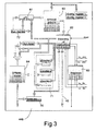
- Figure 3 shows an example of the circuit architecture of the second control stage 44b, which essentially comprises a diagnostic block 60, a first counter block 61, an internal microcontroller 62, a main memory 63, and a secondary memory 64 in which are stored a plurality of parameters which characterize the operation of the electrical injector 12.
- the diagnostic block 60 can make a comparison, instant by instant, between the control signals hs_cmd and ls_cmd supplied at the output, and the feedback signals hs_fbk and ls_fbk received at the input, in such a way as to detect any error conditions and then to generate, in accordance with these errors, the interruption request signal to the internal microcontroller 62 or to the main external microcontroller (not shown).
- the main memory 63 stores the program code containing the various instructions to be implemented in the internal microcontroller 62, and consists of a RAM memory block (256x16) which interacts with the first counter block 61 which stores, instant by instant, the address relating to the instruction to be supplied at the output to the internal microcontroller 62.
- this can "interface" the internal microcontroller with the main external microcontroller, and has the function of storing a plurality of control parameters which characterize the operation of the electrical injector.
- each control block 44 is connected to the synchronization bus 49b to receive from the latter a signal S SINC which encodes a set of data to enable the said control block 44 to synchronize the commands to be sent to the drive circuit 11 with those sent by the other control blocks 44, according to a predetermined common command strategy for the electrical injectors.
- synchronization block 45 this is connected to the four state buses 49a, from which it receives the four corresponding state signals S FLAG , and, in accordance with these, identifies the operating state of each control block 44, so that it can coordinate and synchronize, on the basis of the detected states, the operating actions for the electrical injectors implemented by the said control blocks 44.
- the synchronization block 45 supplies at its output, on the basis of the four state signals S FLAG , the synchronization signal S SINC on the synchronization bus 49b, by means of which the said signal S SINC is supplied to the inputs of the four control blocks 44.
- the synchronization block 45 is also connected by means of an I/O port (not shown) to the communication bus 49c by means of which it receives and/or transmits control signals to or from external control devices (not shown).
- the synchronization block 45 comprises two synchronization logic stages, which can implement a first set of logical operations on the most significant bits (flags) of the state signals S FLAG , denoted below by the abbreviation MSB, and a second set of logical operations on the least significant bits (flags) of the state signals S FLAG , denoted below by the abbreviation LSB.
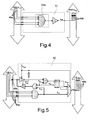
- the synchronization logic stage 51 comprises an AND circuit 51a, which is provided with four inputs connected to the corresponding four state buses 49a to receive the MSBs of the four corresponding state signals S FLAG , and an output connected to the synchronization bus 49b on which it supplies the MSBs of the synchronization signal S SINC .
- the AND circuit 51a is provided with a set of AND logic gates (only one of which is shown schematically in Figure 4), each of which can implement the AND operation between the corresponding MSBs contained in the four state signals S FLAG .
- each logic gate can execute the AND operation between the bits of the four state signals S FLAG which occupy the same coding position within the state signals S FLAG .
- the synchronization logic stage 51 therefore supplies at its output, and transfers to the synchronization bus 49b, the 12 MSBs which make up the synchronization signal S SINC , each of which is obtained by means of the AND operation executed between the four corresponding bits (flags) of the state signals S FLAG .
- the input of the synchronization logic stage 52 is connected to the four state buses 49a to receive the LSBs of the four state signals S FLAG , and its output is connected to the synchronization bus 49b, to which it supplies the 4 LSBs which, together with the 12 MSBs supplied at the output of the synchronization logic stage 51, make up the 16 bits which encode the signal S SINC .
- the synchronization logic stage 52 is also connected to the communication bus 49c to receive and/or transmit the control signals from or to the external devices and/or to the main external microcontroller (not shown), and can operate selectively, according to an command signal S DIR , between a first and a second operating condition.
- the synchronization logic stage 52 implements the logical AND between the corresponding LSBs (flags) of the four state signals S FLAG and supplies the 4 bits (flags) resulting from this operation both at its output, thus completing the synchronization signal S SINC , and to the communication bus 49c, overwriting the LSBs of the control signal with the corresponding 4 bits of the control signal.
- the synchronization logic stage 52 supplies directly on its output the 4 LSBs belonging to the control signal received on the communication bus 49c, thus overwriting the 4 LSBs of the synchronization signal S SINC .
- the synchronization logic stage 52 comprises four logical circuits which are identical with each other (only one of which is shown in Figure 5), each of which can process the four LSBs occupying the same position in the corresponding four state signals S FLAG .
- each logic circuit of the synchronization logic stage 52 comprises an AND logic gate, a multiplexer, a pair of XOR (OR-exclusive) gates, two three-state gates, and a flip-flop.
- the AND logic gate is provided with four inputs, each of which receives an LSB of a corresponding state signal S FLAG and is provided with an output supplying a signal S INT encoding the bit obtained from the AND operation among the four incoming bits; a first XOR gate having a first input connected to the output of the AND gate to receive the signal S INT , a second input for receiving a signal S FP for switching the polarities of the bits, and an output connected to the communication bus 49c by means of a first three-state gate which can be activated by the negated command signal S DIR .
- the second XOR gate has an input connected to the communication bus 49c by means of the second three-state gate which can be activated by the command signal S DIR , a second input receiving the signal S FP and an output connected to the input of the flip-flop.
- this has a first input connected to the output of the flip-flop, a second input connected to the output of the AND gate, an output connected to the synchronization bus 49b, and, finally, a third input receiving the command signal S DIR which selectively activates the connection between the output and one of the two inputs.
- the negated command signal S DIR activates the first three-state gate which connects the output of the first XOR gate to the communication bus 49c, the multiplexer is activated and supplies on its output the signal S INT available on the corresponding first input, while the command signal S DIR switches the second three-state gate to the high-impedance state.
- the signal S INT resulting from the AND operation of the four LSBs of the four input signals is supplied, on the one hand, to the output of the multiplexer, forming one of the LSBs of the signal S SINC , and, on the other hand, following the XOR logic operation (executed by the first XOR logic gate on the basis of the signal S FP ), to the communication bus 49c, in which one LSB of the control signal on the said communication bus 49c is overwritten.
- the command signal S DIR activates the second three-state gate which connects the first input of the second XOR gate to the communication bus 49c and the multiplexer is activated, supplying at its output the signal supplied by the flip-flop.
- the negated command signal S DIR switches the first three-state gate to the high impedance state, thus disabling the output of the first XOR gate and inhibiting the writing of the signal S INT to the communication bus 49c.
- one of the 4 LSBs of the control signal present in the communication bus 49c is received at the input of the second XOR gate, which, following the logic operation, supplies it to the flip-flop, which in turn supplies it through the multiplexer to the synchronization bus 49b, thus causing the overwriting of a corresponding LSB of the signal S SINC .
- the synchronization block 45 is provided not only with the two synchronization logic stages 51 and 52 described above, but also with a set of internal configuration registers, for example: a register containing the information on the polarity to be assigned to the flags according to which the signal S FP is generated; a register containing the information on the read/write "direction" or route to be assigned to the flags, according to which the command signal S DIR is generated; and a register containing the information on the control of the configuration of the bits or flags associated with the current thresholds in the measurement block 47.
- the synchronization block 45 also comprises a first configuration block (not shown), which stores an access mode to the data stored in the internal memories of the control blocks 44 by external devices, such as the main external microcontroller (not shown).
- the synchronization block 45 comprises a malfunction control block (not shown) for receiving interruption request signals (Interrupt) transmitted by the control blocks 44 if a specified condition of malfunction of the electrical injectors is detected.
- a malfunction control block (not shown) for receiving interruption request signals (Interrupt) transmitted by the control blocks 44 if a specified condition of malfunction of the electrical injectors is detected.
- the malfunction control block can receive from each control block 44 a corresponding interruption request signal, and generates at its output, in accordance with these signals, a main interrupt signal, which is transmitted to the main external microcontroller, which identifies the control block(s) 44 which have diagnosed the problem.
- the operation of the drive device 41 can easily be deduced from the above description and requires no special explanation.
- the drive device 41 for electrical actuators is highly advantageous in that it can coordinate the control actions implemented on the electrical injectors by the corresponding control blocks, thus providing a correct synchronization of the activation of the electrical injectors in the various stages of current maintenance and control.
Landscapes
- Engineering & Computer Science (AREA)
- Computer Hardware Design (AREA)
- General Engineering & Computer Science (AREA)
- Microelectronics & Electronic Packaging (AREA)
- Chemical & Material Sciences (AREA)
- Combustion & Propulsion (AREA)
- Mechanical Engineering (AREA)
- Fuel-Injection Apparatus (AREA)
- Electrical Control Of Air Or Fuel Supplied To Internal-Combustion Engine (AREA)
- Electronic Switches (AREA)
- Control Of Electrical Variables (AREA)
- Dc-Dc Converters (AREA)
- Control Of Stepping Motors (AREA)
- Valve Device For Special Equipments (AREA)
- Reciprocating, Oscillating Or Vibrating Motors (AREA)
- Control Of Electric Motors In General (AREA)
Applications Claiming Priority (2)
| Application Number | Priority Date | Filing Date | Title |
|---|---|---|---|
| ITTO20030939 | 2003-11-25 | ||
| IT000939A ITTO20030939A1 (it) | 2003-11-25 | 2003-11-25 | Dispositivo di comando di elettroattuatori induttivi. |
Publications (2)
| Publication Number | Publication Date |
|---|---|
| EP1536123A1 EP1536123A1 (en) | 2005-06-01 |
| EP1536123B1 true EP1536123B1 (en) | 2006-10-11 |
Family
ID=34452292
Family Applications (1)
| Application Number | Title | Priority Date | Filing Date |
|---|---|---|---|
| EP04106052A Expired - Lifetime EP1536123B1 (en) | 2003-11-25 | 2004-11-24 | Drive device for inductive electrical actuators |
Country Status (7)
| Country | Link |
|---|---|
| US (1) | US7280339B2 (it) |
| EP (1) | EP1536123B1 (it) |
| JP (2) | JP4897211B2 (it) |
| AT (1) | ATE342437T1 (it) |
| DE (1) | DE602004002748T2 (it) |
| ES (1) | ES2271787T3 (it) |
| IT (1) | ITTO20030939A1 (it) |
Cited By (1)
| Publication number | Priority date | Publication date | Assignee | Title |
|---|---|---|---|---|
| CN101340141B (zh) * | 2007-07-06 | 2012-02-15 | 日产自动车株式会社 | 功率变换装置 |
Families Citing this family (11)
| Publication number | Priority date | Publication date | Assignee | Title |
|---|---|---|---|---|
| JP3981882B2 (ja) * | 2003-03-05 | 2007-09-26 | 株式会社デンソー | 回路保護装置およびエアバッグシステム |
| US7054737B2 (en) * | 2004-03-18 | 2006-05-30 | Ford Global Technologies, Llc | Power electronics circuit with voltage regulator for electromechanical valve actuator of an internal combustion engine |
| DE102007045508B4 (de) * | 2007-09-24 | 2017-05-11 | Continental Automotive Gmbh | Endstufenvorrichtung zum Steuern einer Fluidzumessvorrichtung |
| DE102010027989A1 (de) * | 2010-04-20 | 2011-10-20 | Robert Bosch Gmbh | Verfahren zum Betreiben einer Brennkraftmaschine, bei dem ein Magnetventil zum Einspritzen von Kraftstoff betätigt wird |
| US9989947B2 (en) * | 2013-08-20 | 2018-06-05 | Infineon Technologies Ag | Driver circuit for driving electromagnetic actuators |
| US9404434B2 (en) * | 2014-01-09 | 2016-08-02 | Infineon Technologies Ag | Universal solenoid driver |
| US10087866B2 (en) | 2015-08-31 | 2018-10-02 | Infineon Technologies Ag | Detecting fuel injector timing with current sensing |
| US10087872B2 (en) | 2015-11-18 | 2018-10-02 | Infineon Technologies Ag | System and method for a synchronized driver circuit |
| EP3220406B1 (en) * | 2016-03-14 | 2018-10-03 | ABB S.p.A. | A coil actuator for lv or mv applications |
| US10184860B2 (en) | 2016-04-08 | 2019-01-22 | Infineon Technologies Ag | Control system for power train control |
| DE102019200179A1 (de) * | 2019-01-09 | 2020-07-09 | Robert Bosch Gmbh | Ansteuervorrichtung für Injektoren |
Family Cites Families (14)
| Publication number | Priority date | Publication date | Assignee | Title |
|---|---|---|---|---|
| FR1485621A (fr) * | 1966-04-13 | 1967-06-23 | Perfectionnements aux dispositifs électroniques d'injecteur et aux injecteurs utilisés avec ces dispositifs | |
| US4327693A (en) * | 1980-02-01 | 1982-05-04 | The Bendix Corporation | Solenoid driver using single boost circuit |
| JPH06213063A (ja) * | 1993-01-19 | 1994-08-02 | Nippondenso Co Ltd | 車両用電子制御装置 |
| JPH07166953A (ja) * | 1994-08-23 | 1995-06-27 | Nippondenso Co Ltd | 制御システムの状態出力装置 |
| SE503397C2 (sv) * | 1994-09-11 | 1996-06-03 | Mecel Ab | Arrangemang och förfarande för ett reglersystem till en förbränningsmotor innefattande ett distribuerat datornät |
| IT1296664B1 (it) * | 1997-12-19 | 1999-07-14 | Fiat Ricerche | Dispositivo di comando di elettroattuatori. |
| FR2776413B1 (fr) * | 1998-03-17 | 2000-05-26 | Renault | Systeme de generation de commandes d'actionneurs |
| DE19813138A1 (de) * | 1998-03-25 | 1999-09-30 | Bosch Gmbh Robert | Verfahren und Vorrichtung zur Ansteuerung eines elektromagnetischen Verbrauchers |
| EP0989297B1 (de) * | 1998-09-21 | 2004-09-29 | Wärtsilä Schweiz AG | Hubkolbenbrennkraftmaschine |
| JP3905247B2 (ja) * | 1999-05-13 | 2007-04-18 | 三菱電機株式会社 | 筒内噴射式インジェクタの制御装置 |
| DE60023446T2 (de) * | 2000-04-01 | 2006-05-18 | Robert Bosch Gmbh | Verfahren und Vorrichtung zur Bestimmung der Ladungsquantität während des Auf- und Entladens von piezoelektrischen Elementen |
| JP4037632B2 (ja) * | 2001-09-28 | 2008-01-23 | 株式会社日立製作所 | 燃料噴射装置を備えた内燃機関の制御装置 |
| ITTO20030940A1 (it) * | 2003-11-25 | 2005-05-26 | Fiat Ricerche | Dispositivo di comando di elettroiniettori di un impianto di iniezione del combustibile a collettore comune per un motore a combustione interna. |
| JP2005180217A (ja) * | 2003-12-16 | 2005-07-07 | Mitsubishi Electric Corp | 筒内噴射式エンジンのインジェクタ制御装置 |
-
2003
- 2003-11-25 IT IT000939A patent/ITTO20030939A1/it unknown
-
2004
- 2004-11-17 US US10/989,726 patent/US7280339B2/en not_active Expired - Lifetime
- 2004-11-24 ES ES04106052T patent/ES2271787T3/es not_active Expired - Lifetime
- 2004-11-24 AT AT04106052T patent/ATE342437T1/de not_active IP Right Cessation
- 2004-11-24 DE DE602004002748T patent/DE602004002748T2/de not_active Expired - Lifetime
- 2004-11-24 EP EP04106052A patent/EP1536123B1/en not_active Expired - Lifetime
- 2004-11-25 JP JP2004341011A patent/JP4897211B2/ja not_active Expired - Fee Related
-
2010
- 2010-02-15 JP JP2010030371A patent/JP2010174893A/ja active Pending
Cited By (1)
| Publication number | Priority date | Publication date | Assignee | Title |
|---|---|---|---|---|
| CN101340141B (zh) * | 2007-07-06 | 2012-02-15 | 日产自动车株式会社 | 功率变换装置 |
Also Published As
| Publication number | Publication date |
|---|---|
| DE602004002748T2 (de) | 2007-08-16 |
| ES2271787T3 (es) | 2007-04-16 |
| JP2005201248A (ja) | 2005-07-28 |
| JP4897211B2 (ja) | 2012-03-14 |
| ITTO20030939A1 (it) | 2005-05-26 |
| US7280339B2 (en) | 2007-10-09 |
| EP1536123A1 (en) | 2005-06-01 |
| ATE342437T1 (de) | 2006-11-15 |
| JP2010174893A (ja) | 2010-08-12 |
| US20050141167A1 (en) | 2005-06-30 |
| DE602004002748D1 (de) | 2006-11-23 |
Similar Documents
| Publication | Publication Date | Title |
|---|---|---|
| JP2010174893A (ja) | 誘導型電気アクチュエータ用の動作装置 | |
| EP1536124B1 (en) | Drive device for electrical injectors of an internal combustion engine common rail fuel injection system | |
| US6016040A (en) | Device and method for driving at least one capacitive actuator | |
| US5130598A (en) | Apparatus for driving a piezoelectric actuator | |
| GB2364576A (en) | A fuel injection conflict monitoring and resolution installation | |
| KR19980702719A (ko) | 한 개 이상의 전자적 부하 제어 장치 | |
| JPH08512436A (ja) | 電磁的負荷を制御する装置及び方法 | |
| JP3955622B2 (ja) | 少なくとも1つの電磁的負荷の制御装置 | |
| US5986360A (en) | Device and method for controlling at least one capacitive actuator | |
| US20140121946A1 (en) | Direct Injection Cross Point Switching for Multiplexing Control in an Engine Control System | |
| US20020035650A1 (en) | Vehicle-mounted electronic control apparatus | |
| US7035728B2 (en) | Drive device for inductive electroactuators | |
| US6081062A (en) | Method and device for driving at least one capacitive actuator | |
| US20140121846A1 (en) | Software Hierarchy for Controlling Multiple Injection Events | |
| KR100886523B1 (ko) | 시스템 파라미터를 제어하기 위한 방법 및 장치 | |
| US9048775B2 (en) | H-bridge for combined solenoid and piezo injection control | |
| EP0685030B1 (en) | Internal combustion engine fuel injector control system | |
| WO2005014992A1 (en) | Method for operating an inductive electroactuator control device | |
| US6943480B2 (en) | System for controlling a piezoelectric actuator, in particular for the fuel injectors of a diesel engine | |
| KR100867480B1 (ko) | 제어 시스템으로 또는 제어 시스템 내에서 제어 파라미터를 제공하는 방법 및 장치 | |
| USRE38470E1 (en) | Method and device for driving at least one capacitive actuator | |
| JP2014098343A (ja) | インジェクタ駆動装置 | |
| JP2014101801A (ja) | インジェクタ駆動装置 | |
| CN1031127A (zh) | 阀门电动装置 | |
| JP2018204524A (ja) | 燃料噴射制御装置 |
Legal Events
| Date | Code | Title | Description |
|---|---|---|---|
| PUAI | Public reference made under article 153(3) epc to a published international application that has entered the european phase |
Free format text: ORIGINAL CODE: 0009012 |
|
| AK | Designated contracting states |
Kind code of ref document: A1 Designated state(s): AT BE BG CH CY CZ DE DK EE ES FI FR GB GR HU IE IS IT LI LU MC NL PL PT RO SE SI SK TR |
|
| AX | Request for extension of the european patent |
Extension state: AL HR LT LV MK YU |
|
| 17P | Request for examination filed |
Effective date: 20051129 |
|
| AKX | Designation fees paid |
Designated state(s): AT BE BG CH CY CZ DE DK EE ES FI FR GB GR HU IE IS IT LI LU MC NL PL PT RO SE SI SK TR |
|
| GRAP | Despatch of communication of intention to grant a patent |
Free format text: ORIGINAL CODE: EPIDOSNIGR1 |
|
| GRAS | Grant fee paid |
Free format text: ORIGINAL CODE: EPIDOSNIGR3 |
|
| GRAA | (expected) grant |
Free format text: ORIGINAL CODE: 0009210 |
|
| AK | Designated contracting states |
Kind code of ref document: B1 Designated state(s): AT BE BG CH CY CZ DE DK EE ES FI FR GB GR HU IE IS IT LI LU MC NL PL PT RO SE SI SK TR |
|
| PG25 | Lapsed in a contracting state [announced via postgrant information from national office to epo] |
Ref country code: IT Free format text: LAPSE BECAUSE OF FAILURE TO SUBMIT A TRANSLATION OF THE DESCRIPTION OR TO PAY THE FEE WITHIN THE PRESCRIBED TIME-LIMIT;WARNING: LAPSES OF ITALIAN PATENTS WITH EFFECTIVE DATE BEFORE 2007 MAY HAVE OCCURRED AT ANY TIME BEFORE 2007. THE CORRECT EFFECTIVE DATE MAY BE DIFFERENT FROM THE ONE RECORDED. Effective date: 20061011 Ref country code: SI Free format text: LAPSE BECAUSE OF FAILURE TO SUBMIT A TRANSLATION OF THE DESCRIPTION OR TO PAY THE FEE WITHIN THE PRESCRIBED TIME-LIMIT Effective date: 20061011 Ref country code: CH Free format text: LAPSE BECAUSE OF FAILURE TO SUBMIT A TRANSLATION OF THE DESCRIPTION OR TO PAY THE FEE WITHIN THE PRESCRIBED TIME-LIMIT Effective date: 20061011 Ref country code: FI Free format text: LAPSE BECAUSE OF FAILURE TO SUBMIT A TRANSLATION OF THE DESCRIPTION OR TO PAY THE FEE WITHIN THE PRESCRIBED TIME-LIMIT Effective date: 20061011 Ref country code: PL Free format text: LAPSE BECAUSE OF FAILURE TO SUBMIT A TRANSLATION OF THE DESCRIPTION OR TO PAY THE FEE WITHIN THE PRESCRIBED TIME-LIMIT Effective date: 20061011 Ref country code: AT Free format text: LAPSE BECAUSE OF FAILURE TO SUBMIT A TRANSLATION OF THE DESCRIPTION OR TO PAY THE FEE WITHIN THE PRESCRIBED TIME-LIMIT Effective date: 20061011 Ref country code: LI Free format text: LAPSE BECAUSE OF FAILURE TO SUBMIT A TRANSLATION OF THE DESCRIPTION OR TO PAY THE FEE WITHIN THE PRESCRIBED TIME-LIMIT Effective date: 20061011 Ref country code: SK Free format text: LAPSE BECAUSE OF FAILURE TO SUBMIT A TRANSLATION OF THE DESCRIPTION OR TO PAY THE FEE WITHIN THE PRESCRIBED TIME-LIMIT Effective date: 20061011 Ref country code: NL Free format text: LAPSE BECAUSE OF FAILURE TO SUBMIT A TRANSLATION OF THE DESCRIPTION OR TO PAY THE FEE WITHIN THE PRESCRIBED TIME-LIMIT Effective date: 20061011 Ref country code: BE Free format text: LAPSE BECAUSE OF FAILURE TO SUBMIT A TRANSLATION OF THE DESCRIPTION OR TO PAY THE FEE WITHIN THE PRESCRIBED TIME-LIMIT Effective date: 20061011 Ref country code: RO Free format text: LAPSE BECAUSE OF FAILURE TO SUBMIT A TRANSLATION OF THE DESCRIPTION OR TO PAY THE FEE WITHIN THE PRESCRIBED TIME-LIMIT Effective date: 20061011 Ref country code: CZ Free format text: LAPSE BECAUSE OF FAILURE TO SUBMIT A TRANSLATION OF THE DESCRIPTION OR TO PAY THE FEE WITHIN THE PRESCRIBED TIME-LIMIT Effective date: 20061011 |
|
| REG | Reference to a national code |
Ref country code: GB Ref legal event code: FG4D |
|
| REG | Reference to a national code |
Ref country code: CH Ref legal event code: EP |
|
| REG | Reference to a national code |
Ref country code: IE Ref legal event code: FG4D |
|
| REF | Corresponds to: |
Ref document number: 602004002748 Country of ref document: DE Date of ref document: 20061123 Kind code of ref document: P |
|
| PG25 | Lapsed in a contracting state [announced via postgrant information from national office to epo] |
Ref country code: IE Free format text: LAPSE BECAUSE OF NON-PAYMENT OF DUE FEES Effective date: 20061124 |
|
| PG25 | Lapsed in a contracting state [announced via postgrant information from national office to epo] |
Ref country code: MC Free format text: LAPSE BECAUSE OF NON-PAYMENT OF DUE FEES Effective date: 20061130 |
|
| REG | Reference to a national code |
Ref country code: SE Ref legal event code: TRGR |
|
| PG25 | Lapsed in a contracting state [announced via postgrant information from national office to epo] |
Ref country code: DK Free format text: LAPSE BECAUSE OF FAILURE TO SUBMIT A TRANSLATION OF THE DESCRIPTION OR TO PAY THE FEE WITHIN THE PRESCRIBED TIME-LIMIT Effective date: 20070111 Ref country code: BG Free format text: LAPSE BECAUSE OF FAILURE TO SUBMIT A TRANSLATION OF THE DESCRIPTION OR TO PAY THE FEE WITHIN THE PRESCRIBED TIME-LIMIT Effective date: 20070111 |
|
| PG25 | Lapsed in a contracting state [announced via postgrant information from national office to epo] |
Ref country code: IS Free format text: LAPSE BECAUSE OF FAILURE TO SUBMIT A TRANSLATION OF THE DESCRIPTION OR TO PAY THE FEE WITHIN THE PRESCRIBED TIME-LIMIT Effective date: 20070211 |
|
| PG25 | Lapsed in a contracting state [announced via postgrant information from national office to epo] |
Ref country code: PT Free format text: LAPSE BECAUSE OF FAILURE TO SUBMIT A TRANSLATION OF THE DESCRIPTION OR TO PAY THE FEE WITHIN THE PRESCRIBED TIME-LIMIT Effective date: 20070319 |
|
| NLV1 | Nl: lapsed or annulled due to failure to fulfill the requirements of art. 29p and 29m of the patents act | ||
| ET | Fr: translation filed | ||
| REG | Reference to a national code |
Ref country code: ES Ref legal event code: FG2A Ref document number: 2271787 Country of ref document: ES Kind code of ref document: T3 |
|
| REG | Reference to a national code |
Ref country code: CH Ref legal event code: PL |
|
| PLBE | No opposition filed within time limit |
Free format text: ORIGINAL CODE: 0009261 |
|
| STAA | Information on the status of an ep patent application or granted ep patent |
Free format text: STATUS: NO OPPOSITION FILED WITHIN TIME LIMIT |
|
| 26N | No opposition filed |
Effective date: 20070712 |
|
| PG25 | Lapsed in a contracting state [announced via postgrant information from national office to epo] |
Ref country code: GR Free format text: LAPSE BECAUSE OF FAILURE TO SUBMIT A TRANSLATION OF THE DESCRIPTION OR TO PAY THE FEE WITHIN THE PRESCRIBED TIME-LIMIT Effective date: 20070112 |
|
| PG25 | Lapsed in a contracting state [announced via postgrant information from national office to epo] |
Ref country code: EE Free format text: LAPSE BECAUSE OF FAILURE TO SUBMIT A TRANSLATION OF THE DESCRIPTION OR TO PAY THE FEE WITHIN THE PRESCRIBED TIME-LIMIT Effective date: 20061011 |
|
| PG25 | Lapsed in a contracting state [announced via postgrant information from national office to epo] |
Ref country code: TR Free format text: LAPSE BECAUSE OF FAILURE TO SUBMIT A TRANSLATION OF THE DESCRIPTION OR TO PAY THE FEE WITHIN THE PRESCRIBED TIME-LIMIT Effective date: 20061011 Ref country code: HU Free format text: LAPSE BECAUSE OF FAILURE TO SUBMIT A TRANSLATION OF THE DESCRIPTION OR TO PAY THE FEE WITHIN THE PRESCRIBED TIME-LIMIT Effective date: 20070412 Ref country code: LU Free format text: LAPSE BECAUSE OF NON-PAYMENT OF DUE FEES Effective date: 20061124 |
|
| PG25 | Lapsed in a contracting state [announced via postgrant information from national office to epo] |
Ref country code: CY Free format text: LAPSE BECAUSE OF FAILURE TO SUBMIT A TRANSLATION OF THE DESCRIPTION OR TO PAY THE FEE WITHIN THE PRESCRIBED TIME-LIMIT Effective date: 20061011 |
|
| PGFP | Annual fee paid to national office [announced via postgrant information from national office to epo] |
Ref country code: GB Payment date: 20101124 Year of fee payment: 7 |
|
| PGFP | Annual fee paid to national office [announced via postgrant information from national office to epo] |
Ref country code: ES Payment date: 20111216 Year of fee payment: 8 Ref country code: SE Payment date: 20111115 Year of fee payment: 8 |
|
| GBPC | Gb: european patent ceased through non-payment of renewal fee |
Effective date: 20121124 |
|
| PG25 | Lapsed in a contracting state [announced via postgrant information from national office to epo] |
Ref country code: SE Free format text: LAPSE BECAUSE OF NON-PAYMENT OF DUE FEES Effective date: 20121125 |
|
| PG25 | Lapsed in a contracting state [announced via postgrant information from national office to epo] |
Ref country code: GB Free format text: LAPSE BECAUSE OF NON-PAYMENT OF DUE FEES Effective date: 20121124 |
|
| REG | Reference to a national code |
Ref country code: ES Ref legal event code: FD2A Effective date: 20140305 |
|
| PG25 | Lapsed in a contracting state [announced via postgrant information from national office to epo] |
Ref country code: ES Free format text: LAPSE BECAUSE OF NON-PAYMENT OF DUE FEES Effective date: 20121125 |
|
| REG | Reference to a national code |
Ref country code: FR Ref legal event code: PLFP Year of fee payment: 12 |
|
| REG | Reference to a national code |
Ref country code: FR Ref legal event code: PLFP Year of fee payment: 13 |
|
| REG | Reference to a national code |
Ref country code: FR Ref legal event code: PLFP Year of fee payment: 14 |
|
| PGFP | Annual fee paid to national office [announced via postgrant information from national office to epo] |
Ref country code: DE Payment date: 20201130 Year of fee payment: 17 Ref country code: FR Payment date: 20201126 Year of fee payment: 17 |
|
| REG | Reference to a national code |
Ref country code: DE Ref legal event code: R119 Ref document number: 602004002748 Country of ref document: DE |
|
| PG25 | Lapsed in a contracting state [announced via postgrant information from national office to epo] |
Ref country code: DE Free format text: LAPSE BECAUSE OF NON-PAYMENT OF DUE FEES Effective date: 20220601 |
|
| PG25 | Lapsed in a contracting state [announced via postgrant information from national office to epo] |
Ref country code: FR Free format text: LAPSE BECAUSE OF NON-PAYMENT OF DUE FEES Effective date: 20211130 |
|
| PGFP | Annual fee paid to national office [announced via postgrant information from national office to epo] |
Ref country code: IT Payment date: 20221020 Year of fee payment: 19 |
|
| PG25 | Lapsed in a contracting state [announced via postgrant information from national office to epo] |
Ref country code: IT Free format text: LAPSE BECAUSE OF NON-PAYMENT OF DUE FEES Effective date: 20231124 |
|
| PG25 | Lapsed in a contracting state [announced via postgrant information from national office to epo] |
Ref country code: IT Free format text: LAPSE BECAUSE OF NON-PAYMENT OF DUE FEES Effective date: 20231124 |