EP1537675B1 - Verfahren und System zur Neumodulation unter Verwendung von Null ZF - Google Patents
Verfahren und System zur Neumodulation unter Verwendung von Null ZF Download PDFInfo
- Publication number
- EP1537675B1 EP1537675B1 EP03749388A EP03749388A EP1537675B1 EP 1537675 B1 EP1537675 B1 EP 1537675B1 EP 03749388 A EP03749388 A EP 03749388A EP 03749388 A EP03749388 A EP 03749388A EP 1537675 B1 EP1537675 B1 EP 1537675B1
- Authority
- EP
- European Patent Office
- Prior art keywords
- signal
- frequency
- reference oscillator
- modulated
- version
- Prior art date
- Legal status (The legal status is an assumption and is not a legal conclusion. Google has not performed a legal analysis and makes no representation as to the accuracy of the status listed.)
- Expired - Lifetime
Links
Images











Classifications
-
- H—ELECTRICITY
- H03—ELECTRONIC CIRCUITRY
- H03D—DEMODULATION OR TRANSFERENCE OF MODULATION FROM ONE CARRIER TO ANOTHER
- H03D7/00—Transference of modulation from one carrier to another, e.g. frequency-changing
- H03D7/16—Multiple-frequency-changing
- H03D7/161—Multiple-frequency-changing all the frequency changers being connected in cascade
-
- H—ELECTRICITY
- H03—ELECTRONIC CIRCUITRY
- H03D—DEMODULATION OR TRANSFERENCE OF MODULATION FROM ONE CARRIER TO ANOTHER
- H03D7/00—Transference of modulation from one carrier to another, e.g. frequency-changing
- H03D7/16—Multiple-frequency-changing
- H03D7/165—Multiple-frequency-changing at least two frequency changers being located in different paths, e.g. in two paths with carriers in quadrature
- H03D7/166—Multiple-frequency-changing at least two frequency changers being located in different paths, e.g. in two paths with carriers in quadrature using two or more quadrature frequency translation stages
-
- H—ELECTRICITY
- H04—ELECTRIC COMMUNICATION TECHNIQUE
- H04L—TRANSMISSION OF DIGITAL INFORMATION, e.g. TELEGRAPHIC COMMUNICATION
- H04L27/00—Modulated-carrier systems
Definitions
- the present invention relates to the field of communications systems. More particularly, the present invention relates to electronic circuitry for use in modulating and demodulating digital communication signals.
- Modulation techniques find wide application in communications systems.
- modulation techniques are used to facilitate the transmission of communications signals over many mediums including wired and wireless systems.
- modulation techniques are used to transmit communications signals over wired systems such as coaxial or twisted pair.
- modulation techniques are used to transmit communications signals over the air such as in microwave or satellite communications.
- CPE customer premise equipment
- a heterodyne technique Prior attempts have been made to solve the problem of translating a modulated signal from a relatively low modulation frequency to a relatively high modulation frequency by using a heterodyne technique.
- a first modulation at a relatively low frequency is implemented for transmitting a communications signal over a cable.
- the signal at the relatively low modulation frequency is then re-modulated to a relatively high frequency.
- the first modulation frequency needs to be low enough in frequency so that the interconnecting cable loss is minimized.
- this heterodyne approach requires carefully designed image rejection filters to achieve adequate frequency translation.
- the first modulation frequency must be as high as possible to make the image rejection filter easier to build which is in conflict with the need to keep the first modulation frequency as low as possible.
- the presence of the image rejection filter greatly reduces the ability to tune the second modulator to an arbitrary frequency. This technique, developed many years ago, is still quite common in many radio products from a variety of manufacturers.
- a second technique places the modulation source at the end of the cable near the microwave transmitter and uses direct conversion to modulate to a relatively high frequency suitable for application to a microwave transmission.
- Direct conversion by its nature allows for a wide tuning variation.
- Data must be transmitted through the cable so that it can be modulated at the other end of the cable. To do this requires additional hardware to detect the data and correct for signal transmission impairments induced by the cable as well as to recover data and the timing information associated with it.
- This direct modulation approach suffers from the fact that data and clock need to be applied to a modulator at the cable end. Therefore, a. modulator is required to drive the cable and a demodulator is required at the cable end to receive the data and regenerate the timing information associated with that data.
- the present invention addresses the foregoing and related issues.
- an arrangement comprising a reference oscillator signal, a first version of a periodic signal based on the reference oscillator signal, an input signal having a first spectral content, a first modulator coupled to receive the first version of the periodic signal and the input signal, wherein the modulator is configured to produce a first modulated signal, a signal assembler configured to assemble the reference oscillator signal and the first modulated signal, a transmission medium configured to carry the assembled first modulated and reference oscillator signals, a signal disassembler receiving from the transmission medium the assembled reference oscillator and first modulated signals, the signal disassembler providing a representation of the reference oscillator signal, a demodulator coupled to the signal disassembler, wherein the demodulator is configured to demodulate the first modulated signal using a second version of the periodic signal to produce an approximation of the input signal.
- an apparatus comprising a first reference oscillator configured to generate a first reference oscillator signal at a first frequency, a device configured to generate a first version of a periodic signal based on the first reference oscillator signal, an input signal having a first spectral content, a first modulator coupled to receive the first version of the periodic signal and the input signal, wherein the modulator is configured to produce a first modulated signal, a transmission medium configured to carry the first modulated signal, a second reference oscillator configured to generate a second reference oscillator signal at a frequency substantially equal to the first frequency, a second device configured to generate a second version of the periodic signal based on the second reference oscillator signal, a demodulator configured to demodulate the representation of the first modulated input signal using the second version of the periodic signal to produce an approximation of the input signal.
- the present invention solves many of the problems of the prior art by providing for a first modulation at an arbitrary frequency and a second modulation at another arbitrary frequency.
- the present invention demodulates the first modulation using the same reference oscillator signal that was used in the first modulation. Because modulation and demodulation are achieved using the same reference oscillator signal, a close approximation of the original signals is achieved. With this close approximation, a subsequent re-modulation can be readily achieved at a second arbitrary frequency and can further be achieved using low-cost synthesizer and modulation components.
- a first modulation is achieved at a first frequency; the first modulation is then demodulated to zero frequency; and, in turn, a second modulation ( i.e ., re-modulation) is achieved at a second frequency.
- a reference oscillator signal is used to generate a first modulation frequency.
- the first modulation frequency is then used to generate a first modulated signal.
- the reference oscillator signal and the modulated signal are then transmitted over the same medium to a destination.
- the reference oscillator signal is used to demodulate the modulated signal to, in effect, generate approximations of the baseband signals.
- a zero frequency demodulation is achieved.
- a second modulation is implemented at an arbitrary frequency.
- a first modulation frequency signal and the modulated signal are transmitted over the same medium to a destination.
- the first modulation frequency signal is used to demodulate the modulated signal to, in effect, generate approximations of the baseband signals.
- a zero frequency demodulation is achieved.
- a second modulation is implemented at an arbitrary frequency.
- the present invention solves many of the problems of traditional approaches.
- the present invention provides for frequency translation of a modulated signal from a first IF to a second IF frequency without the need for image rejection filtering. Because the first and second IF frequencies can be arbitrary and no image rejection filtering is required, a wide tuning variability of the second IF can be realized which, in turn, simplifies a third conversion to microwave RF.
- the function, f ( t ), has Fourier transform, F ( s ) , as shown in Figure 2A such that the bandpass signal x ( t ), has Fourier transform.
- ⁇ as 1 a ⁇ ⁇ s where a is again a scaling factor.
- a periodic signal, z ( t ) 2cos( ⁇ 1 + ⁇ 2 ) t , is provided at input 106 to mixer 104.
- the frequency, ⁇ 2 is a shifting frequency that for the purposes of the present discussion can be a negative value; further note that the amplitude, 2, is chosen for convenience in scaling as will become evident.
- the term 1 2 ⁇ F ⁇ s + 2 ⁇ ⁇ 1 + ⁇ 2 2 ⁇ ⁇ is shown as signal 224 in Figure 2C ; the term 1 2 ⁇ F ⁇ s - 2 ⁇ ⁇ 1 + ⁇ 2 2 ⁇ ⁇ is shown as signal 230; the term 1 2 ⁇ F ⁇ s + ⁇ 2 2 ⁇ ⁇ as signal 226; and the term 1 2 ⁇ F ⁇ s - ⁇ 2 2 ⁇ ⁇ as signal 228.
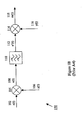
- Mixer 104 of Figure 1A can be used as part of a tuner including single-conversion and dual-conversion tuners. More recently, dual conversion tuners find wide application in telecommunications. In a dual conversion tuner, as the name implies, two conversions (i.e. , two mixers) are implemented. Moreover, in a dual conversion tuner, the input frequency, 2 ⁇ 1 + ⁇ 2 , to bandpass filter 110 is referred to as an image frequency of the desired frequency, ⁇ 2 . The image frequency can sometimes be a problem and therefore needs to be filtered in such tuner applications.
- a first mixer 104 (note that like-numbered components between Figure 1A and Figure 1B operate similarly) up-converts a signal, x ( t ), received at input 102 to a signal, e ( t ), at mixer output 108 having a first intermediate frequency (IF) higher than the frequency of x ( t ).
- the first IF signal, e ( t ) is then filtered by filter 110.
- the filtered signal, e' ( t ) is then at a nominal amplitude while all the rejected signals are at a much lower amplitude.
- the filtered signal, e' ( t ) is then input to a second mixer 114 where mixer 114 mixes signal y ( t ) at input 116 to up-convert the filtered signal, e ' ( t), into a desired IF signal, m(t), at output 118.
- the desired IF signal, m ( t ) is thus the frequency a user desires. In actual implementation, amplification of signals and other factors need to be considered as will be discussed below.
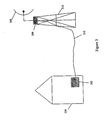
- IDU 302 indoor unit
- ODU 306 outdoor unit
- the desired communications information is usually modulated at a first intermediate frequency (IF) using techniques as described above.
- IF first intermediate frequency
- the IF frequency needs to be low enough in frequency so that the interconnecting cable loss is minimized.
- the desired communications information is modulated at an RF frequency appropriate for transmission over the air also using techniques as described above. Note that two modulations are required to achieve the end result of transmission over the air. This technique is quite common in many radio products from a variety of manufacturers.
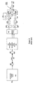
- FIG. 5 Previously, a standard heterodyne architecture has been used such as shown in Figure 5 .
- desired digital communications information is provided at input 501. Such information is then mapped and filtered to produce an in-phase and quadrature signals according to quadrature amplitude modulation (QAM) as shown at block 502.
- QAM quadrature amplitude modulation
- digital-to-analog converters 504 and 506 convert the QAM information into an appropriate baseband signal with frequency content as shown in Figure 4A .
- Low pass filters 508 ( Figure 5 ) and 510 then filter undesired signals to produce a filtered output as shown in Figure 4B .
- the filtered signals are scaled as needed using amplifiers 512 and 514 which produce a scaled version of the signal of Figure 4B .
- the baseband signal is then modulated using a periodic signal having a first frequency.
- the periodic signal is generated at synthesizer or oscillator 516.
- Ninety-degree phase shifting is provided at phase shifter 524.
- Phase shifter 524 then provides phase shifted signals at the first frequency as shown in Figure 4C where the in-phase periodic signal is represented as a real component and the phase shifted periodic signal is represented as an imaginary component. Note that real and imaginary spectral content are represented in solid and dashed lines, respectively.
- the scaled and filtered baseband signals are mixed with the periodic signals at mixers 518 and 520 to generate the modulated in-phase and quadrature signals with spectral content as shown in Figure 4D .
- summer 530 is provided in order to assemble or accumulate multiple modulated signals, however, only one is shown in Figure 5 . Indeed, such a device can be implemented in many ways such as through a summer as shown or a N -plexer as will be described in another embodiment. Moreover, many other types of assemblers, appropriate for use in the present invention, may be developed in the future.
- a divider 534 receives the signals carried on cable 532.
- divider 534 is provided to handle multiple modulated signals.
- Divider 534 can be implemented in many ways. For example, divider 534 can be implemented using filters or a similar N -plexer as used for summer 530.
- Divider 534 provides the appropriate modulated signal (here we have only one) to automatic gain control using (AGC) 536 which amplifies the signal as necessary.
- AGC 536 automatic gain control using the signal is a scaled version of the modulated signal.
- AGC automatic gain control
- a second modulation is implemented.
- Oscillator 540 generates a periodic signal at a second frequency; such signal is then provided to mixer 538.
- the output of mixer 538 is a second modulated signal with undesired spectral content.
- the spectral content of this result is shown in Figure 4E where signals 454 and 456 are desired and signals 450 and 452 are undesired.
- bandpass filter 542 (with filter response 458 as shown in Figure 4E ) is therefore provided to eliminate the undesired signals and produce the desired and scaled, through the use of amplifier 544, output signal with spectral content as shown in Figure 4F .
- the communications information is said to be modulated at a second IF.
- the second modulation at the ODU presents various problems.
- the ODU requires careful attention to image filtering conducted by bandpass filter 542.
- tuning range can become such a problem at certain frequencies that several stages of conversion and tuning become necessary.
- the tuning range of certain oscillators such as oscillator 540 could be as high as 600 MHz, for example, such that any simple conversion to microwave frequencies would put an undesired image frequency within a frequency band of interest unless additional switchable filtering was present.
- the first IF is 100 MHz and the tuning range of the second IF is 600 MHz centered around 2GHz.
- the image will be well within the tuning band requiring multiple image rejection filters with extremely sharp rejection characteristics. Indeed, many filters would have to be switched in and out in order to provide full tuning.
- Another previously known technique places modulation sources at the end of the cable in the ODU near the microwave transceiver.
- This technique uses direct conversion to modulate communications information to a high modulation frequency suitable for application in a microwave transceiver.
- digital communications information is provided at input 601 to block 602 where such information is filtered and amplified.
- Block 602 is typically performed at an IDU.
- the information is passed through a summer 604 in order to accommodate other digital communications inputs.
- the baseband digital information is directed to cable 606 for transmission to an ODU.
- the transmitted signal is received by divider 608 to separate out various streams of information that may have been transmitted over cable 606.
- divider 608 to separate out various streams of information that may have been transmitted over cable 606.
- block 610 Upon dividing out the appropriate stream of information, the transmitted signal is processed at block 610.
- block 610 provides cable equalization and clock recovery.
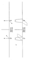
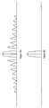
- the problems of direct modulation can be understood with reference to an "eye diagram used in digital communications to visualize how waveforms used to send multiple bits of data can potentially lead to errors in the interpretation of those bits.
- Shown in Figure 7A is a representation of a modulated signal at the input of cable 606.
- Shown in Figure 7B is a representation of the modulated signal received at the other end of cable 606.
- the eye diagram of Figure 7B illustrates the dispersion that can lead to inter-symbol interference as the received signal is distorted.
- the processing at block 610 recovers a clocking signal associated with the received signal and further corrects for its distortion.
- the output of block 610 is therefore an approximation of the signal provided at input 601. Moreover, the output of 610 is provided to a modulation circuit substantially similar to those discussed above.
- the modulation circuit is made up of components 612-636 that are used to modulate at a frequency appropriate for direct input to a microwave RF transceiver.
- Synthesizer 626 generates the appropriate periodic signal for input to the RF transceiver.
- Synthesizer 626 typically has a broader tuning range than does oscillator 540 of Figure 5 such that the scheme of Figure 6 allows for more agile tuning. In fact, direct conversion by its nature allows for a wide tuning variation in the IF frequency. Data, however, must be transmitted through the cable and applied to a cable driver contained within block 602. In doing this, additional hardware such as contained in block 610 is needed to detect the transmitted data and to correct for cable transmission impairments, to recover the transmitted data, and to recover timing information associated with the data. The scheme of Figure 6 is further complicated when various signals are carried on the cable 606. For example, the data rates must be chosen so that the transmitted data signals do not interfere with each other.
- the heterodyne approach requires carefully designed image rejection filters to implement a successful frequency translation.
- This requires that the first IF be as high as possible in order to make the image rejection filter easier to build. But this is in direct conflict with the need to keep the first IF frequency as low as possible to reduce the effects of cable loss.
- the presence of the image reject filter greatly reduces the ability to tune the second IF to whatever frequency is desired.
- the direct modulation also has its disadvantages. It suffers from the fact that data and clock need to be applied to the cable driver such that another modulator of some form is required to drive the cable and a companion demodulator is required at the other end of the cable in order to receive the data and regenerate the timing information associated it.
- the present invention solves many of the problems of such traditional approaches.
- the present invention provides for frequency translation of a modulated signal from an first IF to a second IF frequency without the need for image rejection filtering. Because the first and second IF frequencies can be arbitrary and no image rejection filtering is required, a wide tuning variability of the second IF can be realized which, in turn, simplifies a third conversion to microwave RF.
- a quadrature-modulated signal at a first low IF is transmitted over a length of cable.
- the low IF provides for low cable loss.
- the received signal is translated to a much higher IF that can be applied to a microwave transceiver. The achieved wide tuning range without narrow image filtering requirements makes tuning the final microwave frequency easier with less expensive hardware.
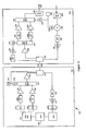
- digital data is provided at input 801 to block 802 where it is mapped and filtered for subsequent quadrature amplitude modulation (OAM) to produce in-phase and quadrature signals according to the QAM format which is as shown at block 502.
- OFAM quadrature amplitude modulation
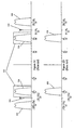
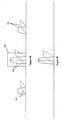
- digital-to-analog converters 804 and 806 convert the QAM information into an appropriate baseband signal with frequency content as shown in Figure 9A .
- Low pass filters 808 and 810 then filter undesired signals to produce a filtered output as shown in Figure 9B .
- the filtered signals are scaled as needed using amplifiers 812 and 814 which produce a scaled version of the signal of Figure 9B .
- the baseband signal is then modulated using a periodic signal at a first IF frequency.
- the periodic signal is generated by means of reference oscillator 816 coupled to synthesizer 818. Synthesizer 818 then generates the periodic signal at a desired first low IF.
- the periodic signal is directed to quadrature phase shifter 824 for appropriate phase shifting. Phase shifter 824 then provides phase shifted periodic signals at a first frequency as shown in Figure 9C .
- the scaled and filtered input signals are then mixed with the periodic signals at mixers 820 and 822 to generate the modulated in-phase and quadrature signals with spectral content as shown in Figure 9D . At this point the information is said to be modulated at a first IF.
- the modulated signals are then summed at summer 826 to generate the composite quadrature modulated signal which is then amplified as necessary at amplifier 828 and directed to another summer 830.
- the present invention further provides the signal from the reference oscillator 816 to summer 830.
- the modulated data signal at a first IF and the reference oscillator signal are both transmitted over cable 832.
- the spectral content of the signals transmitted over cable 832 are as shown in Figure 9D .
- summer 830 is provided in order to accumulate various modulated signals and various reference oscillator signals, however, only one is shown in Figure 8 .
- a signal divider 834 receives the modulated and reference oscillator signals carried on cable 832.
- signal divider 834 and summer 830 are provided to handle various modulated and reference signals.
- Signal divider 834 provides the appropriate modulated signal (here we have only one) to AGC 836 which amplifies the signal as necessary. Also, and in contrast to the prior art heterodyne approach, the divider separates out the reference oscillator signal and provides it to reference bandpass filter 838 to clean up the reference oscillator signal. Moreover, amplification is provided by AGC 840. This processed reference oscillator signal is then provided to synthesizer 842 in much the same manner as reference oscillator 816 signal was provided to synthesizer 818. Through the use of synthesizer 842 in conjunction with components 844 through 856, the received modulated signal is demodulated to baseband in-phase and quadrature signals.
- this demodulation is simply another modulation; the demodulation is achieved by a second modulation using a periodic signal at the same frequency.
- synthesizer 842 receives the reference oscillator signal at the same frequency as synthesizer 818, it can similarly produce the same output frequency which is used to demodulate an already modulated signal.
- the complex demodulated signal is shown in Figure 9E where we note the desired baseband signal 950 with other undesired signals 952 and 954.
- the undesired signals 952 and 954 are filtered out by lowpass filters 850 and 852 to leave only the desired complex baseband signals 956 as shown in Figure 9F .
- Amplifiers 854 and 856 scale the signals shown in Figure 9F .
- the quadrature modulated signals are said to be modulated at zero IF.
- the remaining desired signals present at the outputs of amplifiers 854 and 856 are very close approximations of the original I and Q baseband signals present at the output of amplifiers 812 and 814.
- I ' and Q ' the original signals are referred to as I and Q as shown in Figure 8 .
- synthesizer 864 with a wide tuning range can be used in conjunction with components 858 and 864 to modulate the I ' and Q ' signals to a desired RF signal appropriate for microwave communications.
- circuit delays can cause the constellation pair ( I',Q' ) to appear rotated with respect to the originating constellation pair ( I , Q ).
- the low pass filters 850 and 852 which are wide enough to pass the widest signal frequency, are needed to remove the double frequency components from the demodulator. Low data rates that result in lower bandwidths can therefore use low pass filters with the same bandwidth as for the wideband signals.
- the oscillator frequency ( F osc ) signal, 1016 is transmitted over the cable, for use in demodulation, along with the modulated signal at the first IF frequency.
- the oscillator frequency is divided by an integer, N , which can take on values of 1, 2, 3, etc.
- N the integer
- F osc N x (First IF frequency).
- N the periodic signal from oscillator 1016 is in the passband of the modulated signal at the output of amplifier 1028, and is also transmifted over cable 1032.
- N may place the frequency of oscillator 1016 outside the passband of the modulated signal as seen at the output of summer 1030. Both signals are provided to summer 1030.
- the spectral content of the signals transmitted over cable 1032 is as shown in Figure 11 .
- narrow filter 1036 is used to extract the periodic signal which is amplified by AGC 1038, divided hy signal divider 1039, and then used in conjunction with components 1042 through 1054, in a similar manner as described with reference to Figure 8 , to demodulate the received signal to zero IF.
- the periodic signal is preferably transmitted with amplitude significantly greater than the modulated signal for easier bandpass filtering.
- each zero IF demodulator locks on to its own reference oscillator 1016 and 1090.
- the rest of the block diagram of Figure 10B is essentially the same as that of Figure 10A . It should be noted that because slight frequency errors may occur in generating individual reference oscillator signals, this embodiment may provide less optimal results, but nonetheless quite functional. Whereas RF and microwave applications have been mentioned, it is noted that the present invention can be used for any modulated signal that can have a quadrature representation at zero IF, such as FM, QAM, or PSK (phase shift keying), for instance. It can also simplify some frequency hopping systems.
- an important advantage of the present invention is that it preserves the advantage of direct modulation, for example, facilitating a wide tuning range in a second IF and eliminating the need for image rejection filtering.
- the present invention also addresses problems with direct modulation, for example, the need for data and clock regeneration at the destination end of a cable.
- the present invention provides a way for quadrature modulated data at an arbitrary first IF frequency to be transported over a sizeable length of cable (1000 feet for instance) and to be converted to an arbitrary second IF frequency at the end of the cable without the limitations of image filtering used in heterodyne approaches. Another advantage is that there is no need for data and clock regeneration at the cable end as in the direct modulation approach. Accordingly, the present invention provides for arbitrary first and second IF frequencies. Moreover, no image rejection filtering is required. Indeed, wide band data transmission is possible over cable because the primary modulation is done at the head end of the cable. Also, a wide tuning range of the second IF frequency is achieved with relatively low cost components.
- FIG. 12 Two preferred embodiments of the present invention are shown in Figures 12 and 13 .
- the embodiment of Figure 12 is used for passing wide-bandwidth signals at two different IF frequencies between and IDU and ODU.
- the embodiments shown can be implemented, for example, as QAM modulation with symbol rates at 1xSTM-1 (one channel of Synchronous Transfer Mode-1).
- the embodiment of Figure 13 is similar to that of Figure 12 with some key differences, most notably 2xSTM1 capability.
- STM-1 operates at a gross data rate of 155.52 Mbps such that 1xSTM-1 provides data at such data rate and 2xSTM-1 at twice such data rate.
- the embodiments of the present invention to be described provide cost and power advantages over the prior art and preserve a simplified wide tuning range of the transmitter.
- IDU 1202 the IDU Bus 1206 and IDU interface 1208 provide digital data to QAM mapping and filter module 1210 in a manner consistent with Figures 8 and 10 .
- QAM mapping and filter module 1210 is a VANTEX chip produced by Stratex Networks of San Jose, California. Also appropriate are other QAM receivers with adaptive equalization capable of correcting quadrature errors and I / Q imbalances.
- the operation of components 1212 through 1232 also have direct correspondence to Figure 8 such that it is readily understood a modulated signal and a reference oscillator signal are carried on cable 1212.
- modulator 1224 note that it is set to baseband mode.
- reference oscillator 1228 operates at 10.7 MHz and the I and Q signals are modulated using a 310 MHz signal generated by synthesizer 1226.
- Demodulation in ODU 1204 is accomplished by components 1244 through 1262 in much the same manner as described with reference to Figure 8 .
- the received signal is demodulated to a zero frequency IF with an inexpensive I / Q quadrature demodulator 1252 and a using synthesizer 1254 operating at 310 MHz.
- this PLL uses the same 10.7 MHz reference as the one in the IDU 1202.
- the reference frequency at 10.7 MHz can be easily filtered by an inexpensive ceramic filter 1248, which is the reason for choosing that reference frequency.
- FIG. 12 further detail is shown with regard to the manner of modulating the zero IF signals, I' and Q' , that are present at the output of amplifiers 1260 and 1262.
- modulator 1264 modulates the I' and Q' signals to an appropriate RF and then directs such signals to transmitter circuit 1266 which then provides transceiver signal 1268.
- the resulting zero IF signals, I ' and Q' will not be constantly changing in phase (sometimes called rotating). Instead, there is a fixed phase angle of rotation on the signal dependent upon IDU 1202 to ODU 1204 cable longth
- transceiver signal 1284 may also carry a received signal containing communications information.
- Components 1270 through 1282 are used to down convert to a 125 MHz IF.
- the received signal is sent down the cable to IDU 1202 where it is demodulated using components 1234 through 1240. After demodulation at demodulator 1240, digital information is passed through IDU interface 1208 and, in turn, to IDU bus 1206.
- IDU 1302 has no significant change except for baseband filters 1340 and 1342 that might have to be switch selectable in bandwidth to accommodate various high data rate wide bandwidths signals, but no manufacturing change would be required. Importantly, no changes are needed in ODU 1304, except to pass the widest bandwidth signal. Moreover, because demodulation components are typically contained on a plug-in card, IDU 1302 is configured to simply accept multiple, demodulator cards containing, for example, components 1340 through 1350.
- the present invention provides for generating modulated I and Q signals at a first frequency for transmission over a medium. Moreover, the present invention provides for also transmitting a periodic signal or a signal used to produce such periodic signal over the same medium.
- demodulating circuitry uses the received periodic signal (or the received signal used to produce the periodic signal) to demodulate the received modulated signal.
- the present invention demodulates the received modulated signal to zero IF such that approximations, I ' and Q ', are generated of the original I and Q signals. With such approximations, re-modulation at another arbitrary frequency is possible using relatively inexpensive components while providing for a wide modulation range.
Landscapes
- Engineering & Computer Science (AREA)
- Power Engineering (AREA)
- Computer Networks & Wireless Communication (AREA)
- Signal Processing (AREA)
- Digital Transmission Methods That Use Modulated Carrier Waves (AREA)
- Transmitters (AREA)
- Stabilization Of Oscillater, Synchronisation, Frequency Synthesizers (AREA)
- Amplifiers (AREA)
- Amplitude Modulation (AREA)
Claims (24)
- Vorrichtung, die aufweist:einen Referenzoszillator (816; 1016), der zum Erzeugen eines Referenzoszillatorsignals bei einer ersten Frequenz konfiguriert ist;eine erste Frequenzwechselvorrichtung (818; 1018), die zum Erzeugen einer ersten Version eines periodischen Signals bei einer zweiten Frequenz basierend auf dem Referenzoszillatorsignal;ein Eingangssignal mit einem ersten spektralen Inhalt;einen ersten Modulator (820, 822; 1020, 1022), der gekoppelt ist, um die erste Version des periodischen Signals und das Eingangssignal zu empfangen, wenn der Modulator zum Erzeugen eines ersten modulierten Signals konfiguriert ist;einen Signal-Assembler (830; 1030), der zum Zusammensetzen des Referenzoszillatorsignals und des ersten modulierten Signals konfiguriert ist;ein Übertragungsmedium (832; 1032), das zum Übertragen des zusammengesetzten ersten modulierten Signals und des Referenzoszillatorsignals konfiguriert ist;einen Signal-Disassembler (834; 1034), der vom Übertragungsmedium (832; 1032) das aus dem Referenzoszillatorsignal (816; 1016) und dem ersten modulierten Signal zusammengesetzte Signal empfängt, wobei der Signal-Disassembler (834; 1034) eine Darstellung des Referenzoszillatorsignals liefert;eine zweite Frequenzwechselvorrichtung (842; 1039), die zum Erzeugen einer zweiten Version des periodischen Signals bei der zweiten Frequenz basierend auf der Darstellung des Referenzoszillatorsignals konfiguriert ist;einen Demodulator (844, 846; 1042, 1044), der an den Signal-Disassembler (834; 1034) gekoppelt ist, während der Demodulator zum Demodulieren des ersten modulierten Signals unter Verwendung der zweiten Version des periodischen Signals konfiguriert ist, um eine Näherung des Eingangssignals zu erzeugen; undeinen zweiten Modulator (858, 860; 1056, 1060), der zum Empfangen der Näherung des Eingangssignals vom Demodulator und zum Modulieren der Näherung des Eingangssignals bei einer dritten Frequenz konfiguriert ist.
- Vorrichtung nach Anspruch 1, die des Weiteren einen Verstärker (828; 1028) aufweist, der zum Empfangen des ersten modulierten Signals und des Referenzsignals und zum Verstärken des ersten modulierten Signals und des Referenzoszillatorsignals konfiguriert ist.
- Vorrichtung nach Anspruch 1, wobei der Signal-Assembler eine Vorrichtung aufweist, die aus einer Gruppe bestehend aus einer Summiereinrichtung (830; 1030) und einem N-Plexer ausgewählt ist.
- Vorrichtung nach Anspruch 1, wobei der Signal-Disassembler (834; 1034) eine Vorrichtung aufweist, die aus einer Gruppe bestehend aus einem Bandpassfilter und einem N-Plexer ausgewählt ist.
- Vorrichtung, die aufweist:einen ersten Referenzoszillator (1016), der zum Erzeugen eines ersten Referenzoszillatorsignals bei einer ersten Frequenz konfiguriert ist;einer ersten Frequenzwechseleinrichtung, die zum Erzeugen einer ersten Version eines periodischen Signals bei einer zweiten Frequenz basierend auf dem ersten Referenzoszillatorsignal konfiguriert ist;ein Eingangssignal mit einem ersten spektralen Inhalt;einen ersten Modulator (1020; 1024), der gekoppelt ist, um die erste Version des periodischen Signals und des Eingangssignals zu empfangen, wobei der Modulator zum Erzeugen eines ersten modulierten Signals konfiguriert ist;ein Übertragungsmedium (1032), das zum Übertragen des ersten modulierten Signals konfiguriert ist;einen zweiten Referenzoszillator (1080), der zum Erzeugen eines zweiten Referenzoszillatorsignals mit einer Frequenz konfiguriert ist, die im Wesentlichen gleich der ersten Frequenz ist;einer zweiten Frequenzwechseleinrichtung (1039), die zum Erzeugen einer zweiten Version des periodischen Signals bei einer Frequenz, die im Wesentlichen gleich der zweiten Frequenz ist, basierend auf dem zweiten Referenzoszillatorsignal konfiguriert ist;ein Demodulator (1042, 1044), der zum Demodulieren einer Darstellung des ersten modulierten Eingangssignals unter Verwendung der zweiten Version des periodischen Signals konfiguriert ist, um eine Näherung des Eingangssignals zu erzeugen; undeinen zweiten Modulator (1056, 1062), der zum Empfangen der Näherung des Eingangssignals vom Demodulator und zum Modulieren der Näherung des Eingangssignals bei einer dritten Frequenz konfiguriert ist.
- Vorrichtung nach Anspruch 1 oder 5, wobei die erste Frequenzwechseleinrichtung aus einer Gruppe bestehend aus einem Synthesizer und einem Frequenzteiler ausgewählt ist.
- Vorrichtung nach Anspruch 1 oder 5, wobei die zweite Frequenzwechseleinrichtung aus einer Gruppe bestehend aus einem Synthesizer und einem Frequenzteiler ausgewählt ist.
- Vorrichtung nach Anspruch 5, die des Weiteren einen Verstärker (1028) zum Empfangen der Darstellung des ersten modulierten Eingangssignals von dem Demodulator zwecks Verstärkung der Darstellung des ersten modulierten Eingangssignals aufweist.
- Vorrichtung nach Anspruch 1 oder 5, wobei das Eingangssignal, welches durch den ersten Modulator empfangen wird, ein Quadraturamplitudenmoduliertes Signal QAM ist.
- Vorrichtung nach Anspruch 1 oder 5, wobei das Übertragungsmedium aus einer Gruppe bestehend aus einer Leitung, Luft und Vakuum ausgewählt ist.
- Verfahren zum Erzeugen eines Signals, das die folgenden Schritte aufweist:Erzeugen eines Referenzoszillatorsignals bei einer ersten Frequenz;Erzeugen einer ersten Version eines periodischen Signals bei einer zweiten Frequenz unter Verwendung des Referenzoszillatorsignals;Erzeugen eines Eingangssignals, das einen ersten spektralen Inhalt aufweist;Modulieren des Eingangssignals unter Verwendung der ersten Version des periodischen Signals, um ein erstes moduliertes Eingangssignal zu erzeugen;Zusammensetzen des Referenzoszillatorsignals und des ersten modulierten Eingangssignals;Übertragen des aus dem ersten modulierten Eingangssignal und dem Referenzoszillatorsignal zusammengesetzten Signals über ein Übertragungsmedium;Zerlegen des übertragenen, aus dem Referenzoszillatorsignal und dem ersten modulierten Eingangssignal zusammengesetzten Signals, um eine Darstellung des Referenzoszillatorsignals vorzusehen;Erzeugen einer zweiten Version des periodischen Signals bei der zweiten Frequenz unter Verwendung der Darstellung des Referenzoszillatorsignals; Demodulieren einer Darstellung des ersten modulierten Eingangssignals unterVerwendung des empfangenen Referenzoszillatorsignals, um eine Näherung des Eingangssignals zu erzeugen; undModulieren der Näherung des Eingangssignals bei einer dritten Frequenz.
- Verfahren nach Anspruch 11, wobei das Erzeugen der ersten Version des periodischen Signals ein Zusammenfügen des Referenzoszillatorsignals aufweist.
- Verfahren nach Anspruch 11, wobei das Erzeugen der ersten Version des periodischen Signals ein Teilen der ersten Frequenz des Referenzoszillatorsignals aufweist.
- Verfahren nach Anspruch 11, wobei das Erzeugen der zweiten Version des periodischen Signals ein Zusammenfügen der Darstellung des Referenzoszillatorsignals aufweist.
- Verfahren nach Anspruch 11, wobei das Erzeugen der zweiten Version des periodischen Signals ein Teilen einer Frequenz der Darstellung des Referenzoszillatorsignals aufweist.
- Verfahren nach Anspruch 11, das nach einer Demodulation des Weiteren ein Verstärken der Darstellung des ersten modulierten Eingangssignals und des periodischen Signals aufweist.
- Verfahren zum Erzeugen eines Signals, das die Schritte aufweist:Erzeugen eines ersten Referenzoszillatorsignals bei einer ersten Frequenz;Erzeugen einer ersten Version eines periodischen Signals bei einer zweiten Frequenz unter Verwendung des Referenzoszillatorsignals;Erzeugen eines Eingangssignals mit einem ersten spektralen Inhalt;Modulieren des Eingangssignals unter Verwendung der ersten Version des periodischen Signals, um ein erstes moduliertes Eingangssignal zu erzeugen;Übertragen des ersten modulierten Eingangssignals über ein Übertragungsmedium;Erzeugen eines zweiten Referenzoszillatorsignals bei einer Frequenz, die im Wesentlichen gleich der ersten Frequenz ist;Erzeugen einer zweiten Version des periodischen Signals bei einer Frequenz, die im Wesentlichen gleich der zweiten Frequenz ist, unter Verwendung des zweiten Referenzoszillatorsignals;Demodulieren einer Darstellung des ersten modulierten Eingangssignals unter Verwendung der zweiten Version des periodischen Signals, um eine Näherung des Eingangssignals zu erzeugen; undModulieren der Näherung des Eingangssignals bei einer zweiten Frequenz.
- Verfahren nach Anspruch 17, wobei das Erzeugen der ersten Version des periodischen Signals ein Zusammenfügen des ersten Referenzoszillatorsignals aufweist.
- Verfahren nach Anspruch 17, wobei das Erzeugen der ersten Version des periodischen Signals ein Teilen der ersten Frequenz des ersten Referenzoszillatorsignals aufweist.
- Verfahren nach Anspruch 17, wobei ein Erzeugen der zweiten Version des periodischen Signals ein Zusammenfügen des zweiten Referenzoszillatorsignals aufweist.
- Verfahren nach Anspruch 17, wobei das Erzeugen der zweiten Version des periodischen Signals ein Teilen der Frequenz aufweist, die im Wesentlichen gleich der ersten Frequenz des zweiten Referenzoszillatorsignals ist.
- Verfahren nach Anspruch 17, das des Weiteren nach dem Erzeugen des zweiten Referenzoszillatorsignals ein Verstärken des übertragenen ersten modulierten Eingangssignals und des zweiten Referenzoszillatorsignals aufweist.
- Verfahren nach Anspruch 11 oder 17, wobei das erzeugte Eingangssignal mit dem ersten spektralen Inhalt ein Quadraturenamplituden-moduliertes Signal QAM ist.
- Verfahren nach Anspruch 11 oder 17, wobei die Übertragung über ein Medium erreicht wird, welches aus einer Gruppe bestehend aus einer Leitung, Luft und Vakuum ausgewählt ist.
Priority Applications (1)
| Application Number | Priority Date | Filing Date | Title |
|---|---|---|---|
| SI200332117T SI1537675T1 (sl) | 2002-09-13 | 2003-09-05 | Postopek in sistem za remoduliranje z uporabo ničelne medfrekvence (zero IF) |
Applications Claiming Priority (5)
| Application Number | Priority Date | Filing Date | Title |
|---|---|---|---|
| US41056702P | 2002-09-13 | 2002-09-13 | |
| US410567P | 2002-09-13 | ||
| US350468 | 2003-01-23 | ||
| US10/350,468 US6844787B2 (en) | 2002-09-13 | 2003-01-23 | Method and apparatus for re-modulation using zero IF |
| PCT/US2003/027630 WO2004025844A1 (en) | 2002-09-13 | 2003-09-05 | Method and system for re-modulation using zero if |
Publications (3)
| Publication Number | Publication Date |
|---|---|
| EP1537675A1 EP1537675A1 (de) | 2005-06-08 |
| EP1537675A4 EP1537675A4 (de) | 2008-11-05 |
| EP1537675B1 true EP1537675B1 (de) | 2011-12-14 |
Family
ID=31996989
Family Applications (1)
| Application Number | Title | Priority Date | Filing Date |
|---|---|---|---|
| EP03749388A Expired - Lifetime EP1537675B1 (de) | 2002-09-13 | 2003-09-05 | Verfahren und System zur Neumodulation unter Verwendung von Null ZF |
Country Status (7)
| Country | Link |
|---|---|
| US (1) | US6844787B2 (de) |
| EP (1) | EP1537675B1 (de) |
| CN (1) | CN100395958C (de) |
| AT (1) | ATE537610T1 (de) |
| AU (1) | AU2003268423A1 (de) |
| SI (1) | SI1537675T1 (de) |
| WO (1) | WO2004025844A1 (de) |
Families Citing this family (19)
| Publication number | Priority date | Publication date | Assignee | Title |
|---|---|---|---|---|
| WO2007046877A2 (en) * | 2005-10-12 | 2007-04-26 | Thomson Licensing | Cable remodulator |
| US20080102761A1 (en) * | 2006-10-27 | 2008-05-01 | Stratex Networks, Inc. | System and method for compensation of phase hits |
| DE102007055529A1 (de) * | 2007-08-06 | 2009-02-12 | Rhode & Schwarz Gmbh & Co. Kg | Verfahren und Anordnung zum Erzeugen eines frequenzmodulierten Signals |
| US9008593B2 (en) * | 2010-09-30 | 2015-04-14 | Broadcom Corporation | Method and system for 60 GHz distributed communication |
| US8942645B2 (en) * | 2010-09-30 | 2015-01-27 | Broadcom Corporation | Method and system for communication via subbands in a 60 GHZ distributed communication system |
| US8942646B2 (en) * | 2010-09-30 | 2015-01-27 | Broadcom Corporation | Method and system for a 60 GHz communication device comprising multi-location antennas for pseudo-beamforming |
| US8977219B2 (en) * | 2010-09-30 | 2015-03-10 | Broadcom Corporation | Method and system for mitigating leakage of a 60 GHz transmitted signal back into an RF input of a 60 GHz device |
| US9002300B2 (en) * | 2010-09-30 | 2015-04-07 | Broadcom Corporation | Method and system for time division duplexing (TDD) in a 60 GHZ distributed communication system |
| US8942647B2 (en) * | 2010-09-30 | 2015-01-27 | Broadcom Corporation | Method and system for antenna switching for 60 GHz distributed communication |
| US8913951B2 (en) * | 2007-09-30 | 2014-12-16 | Broadcom Corporation | Method and system for 60 GHz distributed communication utilizing a mesh network of repeaters |
| US7945217B2 (en) * | 2007-11-13 | 2011-05-17 | Provigent Ltd. | Multi-mode baseband-IF converter |
| US7991368B2 (en) * | 2007-12-27 | 2011-08-02 | Provigent Ltd | Integrated RF-IF converter |
| US20110053536A1 (en) | 2009-09-03 | 2011-03-03 | Provigent Ltd | Receiver with re-demodulation |
| US8532237B2 (en) * | 2010-02-09 | 2013-09-10 | Provigent Ltd | Correction of alternating I/Q imbalance and frequency offset impairments |
| US8565352B2 (en) * | 2010-05-03 | 2013-10-22 | Telefonaktiebolaget L M Ericsson (Publ) | Digital IQ imbalance compensation for dual-carrier double conversion receiver |
| US8750441B2 (en) * | 2010-12-20 | 2014-06-10 | Texas Instruments Incorporated | Signal cancellation to reduce phase noise, period jitter, and other contamination in local oscillator, frequency timing, or other timing generators or signal sources |
| US8406709B2 (en) * | 2011-02-27 | 2013-03-26 | Provigent Ltd. | Carrier recovery in re-modulation communication systems |
| SG11201400983YA (en) | 2011-09-26 | 2014-06-27 | Aviat Networks Inc | Systems and methods for asynchronous re-modulation with adaptive i/q adjustment |
| CN116470854B (zh) * | 2023-06-19 | 2023-09-05 | 成都世源频控技术股份有限公司 | 一种宽带变频自适应均衡瞬时带内平坦度装置 |
Family Cites Families (6)
| Publication number | Priority date | Publication date | Assignee | Title |
|---|---|---|---|---|
| US31295A (en) | 1861-02-05 | Guard to flat-irons | ||
| USRE31295E (en) * | 1971-03-01 | 1983-06-28 | Bell Telephone Laboratories, Incorporated | Carrier supply for frequency division multiplexed systems |
| DE2221892C2 (de) * | 1972-05-04 | 1979-12-20 | Siemens Ag, 1000 Berlin U. 8000 Muenchen | Schaltungsanordnung zur Trägerriickgewinnung bei TF-Video- und Datenübertragungssystemen |
| JPH0298238A (ja) * | 1988-10-04 | 1990-04-10 | Nec Corp | 無線通信装置 |
| KR960038686A (ko) * | 1995-04-13 | 1996-11-21 | 김광호 | 단일 주파수에 의한 신호 송수신회로 |
| WO1997040590A1 (en) * | 1996-04-19 | 1997-10-30 | Lgc Wireless, Inc. | Distribution of radio-frequency signals through low bandwidth infrastructures |
-
2003
- 2003-01-23 US US10/350,468 patent/US6844787B2/en not_active Expired - Lifetime
- 2003-09-05 EP EP03749388A patent/EP1537675B1/de not_active Expired - Lifetime
- 2003-09-05 WO PCT/US2003/027630 patent/WO2004025844A1/en not_active Ceased
- 2003-09-05 CN CNB038103966A patent/CN100395958C/zh not_active Expired - Lifetime
- 2003-09-05 SI SI200332117T patent/SI1537675T1/sl unknown
- 2003-09-05 AU AU2003268423A patent/AU2003268423A1/en not_active Abandoned
- 2003-09-05 AT AT03749388T patent/ATE537610T1/de active
Also Published As
| Publication number | Publication date |
|---|---|
| SI1537675T1 (sl) | 2012-08-31 |
| US6844787B2 (en) | 2005-01-18 |
| CN100395958C (zh) | 2008-06-18 |
| WO2004025844A1 (en) | 2004-03-25 |
| ATE537610T1 (de) | 2011-12-15 |
| EP1537675A1 (de) | 2005-06-08 |
| EP1537675A4 (de) | 2008-11-05 |
| AU2003268423A1 (en) | 2004-04-30 |
| CN1653701A (zh) | 2005-08-10 |
| US20040051598A1 (en) | 2004-03-18 |
Similar Documents
| Publication | Publication Date | Title |
|---|---|---|
| EP1537675B1 (de) | Verfahren und System zur Neumodulation unter Verwendung von Null ZF | |
| US5412351A (en) | Quadrature local oscillator network | |
| US8626082B2 (en) | Polar feedback receiver for modulator | |
| US5495500A (en) | Homodyne radio architecture for direct sequence spread spectrum data reception | |
| US10090971B2 (en) | Systems and methods for asynchronous re-modulation with adaptive I/Q adjustment | |
| US6741139B2 (en) | Optical to microwave converter using direct modulation phase shift keying | |
| US7177372B2 (en) | Method and apparatus to remove effects of I-Q imbalances of quadrature modulators and demodulators in a multi-carrier system | |
| EP1335512B1 (de) | Signalvorverarbeitung der überlagerten Signale in einem digitalen Modulationsschema mit überlagerten Signalen zur Verwendung von bestehenden Empfängern | |
| US7426243B2 (en) | Preprocessing signal layers in a layered modulation digital signal system to use legacy receivers | |
| JP3432156B2 (ja) | 変調された単側波帯信号を生成する方法および装置 | |
| JPH11500882A (ja) | 位相変調器及び周波数逓倍器を備えた送信器を用いる伝送システム | |
| Henderson et al. | Microwave mixer technology and applications | |
| US6671337B1 (en) | Carrier modulator for use in a transmitter or transceiver | |
| US6693969B1 (en) | Phase-locked loop methods and structures for generating modulated communication signals with nonconstant envelopes | |
| US6301310B1 (en) | Efficient implementation for systems using CEOQPSK | |
| CN100477544C (zh) | 用于频率转换的设备和方法 | |
| NO318457B1 (no) | Frekvensomformerkrets for millimeterbolgeradio og fremgangsmate derved | |
| JPH08510612A (ja) | 無線トランシーバ回路および無線方法 | |
| US6496079B1 (en) | Optical to microwave converter using direct modulation phase shift keying | |
| US20040151237A1 (en) | Satellite communications system | |
| JP2001103104A (ja) | ディジタル無線装置 | |
| JPH0774790A (ja) | 非線形歪補償送受信回路 | |
| KR100285756B1 (ko) | 무선전송장비에서캐리어트래킹장치 | |
| JP2001044859A (ja) | 送信機 |
Legal Events
| Date | Code | Title | Description |
|---|---|---|---|
| PUAI | Public reference made under article 153(3) epc to a published international application that has entered the european phase |
Free format text: ORIGINAL CODE: 0009012 |
|
| 17P | Request for examination filed |
Effective date: 20041116 |
|
| AK | Designated contracting states |
Kind code of ref document: A1 Designated state(s): AT BE BG CH CY CZ DE DK EE ES FI FR GB GR HU IE IT LI LU MC NL PT RO SE SI SK TR |
|
| AX | Request for extension of the european patent |
Extension state: AL LT LV MK |
|
| DAX | Request for extension of the european patent (deleted) | ||
| A4 | Supplementary search report drawn up and despatched |
Effective date: 20081008 |
|
| RIC1 | Information provided on ipc code assigned before grant |
Ipc: H04J 1/06 20060101ALI20081001BHEP Ipc: H04B 1/00 20060101AFI20040327BHEP |
|
| 17Q | First examination report despatched |
Effective date: 20091020 |
|
| GRAP | Despatch of communication of intention to grant a patent |
Free format text: ORIGINAL CODE: EPIDOSNIGR1 |
|
| RTI1 | Title (correction) |
Free format text: METHOD AND SYSTEM FOR RE-MODULATION USING ZERO IF |
|
| GRAS | Grant fee paid |
Free format text: ORIGINAL CODE: EPIDOSNIGR3 |
|
| GRAA | (expected) grant |
Free format text: ORIGINAL CODE: 0009210 |
|
| AK | Designated contracting states |
Kind code of ref document: B1 Designated state(s): AT BE BG CH CY CZ DE DK EE ES FI FR GB GR HU IE IT LI LU MC NL PT RO SE SI SK TR |
|
| REG | Reference to a national code |
Ref country code: GB Ref legal event code: FG4D |
|
| REG | Reference to a national code |
Ref country code: CH Ref legal event code: EP |
|
| RAP2 | Party data changed (patent owner data changed or rights of a patent transferred) |
Owner name: STRATEX NETWORKS INC. |
|
| REG | Reference to a national code |
Ref country code: IE Ref legal event code: FG4D |
|
| REG | Reference to a national code |
Ref country code: DE Ref legal event code: R096 Ref document number: 60339408 Country of ref document: DE Effective date: 20120209 |
|
| REG | Reference to a national code |
Ref country code: NL Ref legal event code: VDEP Effective date: 20111214 |
|
| PG25 | Lapsed in a contracting state [announced via postgrant information from national office to epo] |
Ref country code: NL Free format text: LAPSE BECAUSE OF FAILURE TO SUBMIT A TRANSLATION OF THE DESCRIPTION OR TO PAY THE FEE WITHIN THE PRESCRIBED TIME-LIMIT Effective date: 20111214 Ref country code: SE Free format text: LAPSE BECAUSE OF FAILURE TO SUBMIT A TRANSLATION OF THE DESCRIPTION OR TO PAY THE FEE WITHIN THE PRESCRIBED TIME-LIMIT Effective date: 20111214 Ref country code: GR Free format text: LAPSE BECAUSE OF FAILURE TO SUBMIT A TRANSLATION OF THE DESCRIPTION OR TO PAY THE FEE WITHIN THE PRESCRIBED TIME-LIMIT Effective date: 20120315 |
|
| PG25 | Lapsed in a contracting state [announced via postgrant information from national office to epo] |
Ref country code: CY Free format text: LAPSE BECAUSE OF FAILURE TO SUBMIT A TRANSLATION OF THE DESCRIPTION OR TO PAY THE FEE WITHIN THE PRESCRIBED TIME-LIMIT Effective date: 20111214 Ref country code: BE Free format text: LAPSE BECAUSE OF FAILURE TO SUBMIT A TRANSLATION OF THE DESCRIPTION OR TO PAY THE FEE WITHIN THE PRESCRIBED TIME-LIMIT Effective date: 20111214 |
|
| PG25 | Lapsed in a contracting state [announced via postgrant information from national office to epo] |
Ref country code: CZ Free format text: LAPSE BECAUSE OF FAILURE TO SUBMIT A TRANSLATION OF THE DESCRIPTION OR TO PAY THE FEE WITHIN THE PRESCRIBED TIME-LIMIT Effective date: 20111214 Ref country code: EE Free format text: LAPSE BECAUSE OF FAILURE TO SUBMIT A TRANSLATION OF THE DESCRIPTION OR TO PAY THE FEE WITHIN THE PRESCRIBED TIME-LIMIT Effective date: 20111214 Ref country code: BG Free format text: LAPSE BECAUSE OF FAILURE TO SUBMIT A TRANSLATION OF THE DESCRIPTION OR TO PAY THE FEE WITHIN THE PRESCRIBED TIME-LIMIT Effective date: 20120314 Ref country code: SK Free format text: LAPSE BECAUSE OF FAILURE TO SUBMIT A TRANSLATION OF THE DESCRIPTION OR TO PAY THE FEE WITHIN THE PRESCRIBED TIME-LIMIT Effective date: 20111214 |
|
| PG25 | Lapsed in a contracting state [announced via postgrant information from national office to epo] |
Ref country code: PT Free format text: LAPSE BECAUSE OF FAILURE TO SUBMIT A TRANSLATION OF THE DESCRIPTION OR TO PAY THE FEE WITHIN THE PRESCRIBED TIME-LIMIT Effective date: 20120416 Ref country code: RO Free format text: LAPSE BECAUSE OF FAILURE TO SUBMIT A TRANSLATION OF THE DESCRIPTION OR TO PAY THE FEE WITHIN THE PRESCRIBED TIME-LIMIT Effective date: 20111214 |
|
| REG | Reference to a national code |
Ref country code: AT Ref legal event code: MK05 Ref document number: 537610 Country of ref document: AT Kind code of ref document: T Effective date: 20111214 |
|
| PLBE | No opposition filed within time limit |
Free format text: ORIGINAL CODE: 0009261 |
|
| STAA | Information on the status of an ep patent application or granted ep patent |
Free format text: STATUS: NO OPPOSITION FILED WITHIN TIME LIMIT |
|
| PG25 | Lapsed in a contracting state [announced via postgrant information from national office to epo] |
Ref country code: DK Free format text: LAPSE BECAUSE OF FAILURE TO SUBMIT A TRANSLATION OF THE DESCRIPTION OR TO PAY THE FEE WITHIN THE PRESCRIBED TIME-LIMIT Effective date: 20111214 |
|
| 26N | No opposition filed |
Effective date: 20120917 |
|
| REG | Reference to a national code |
Ref country code: DE Ref legal event code: R097 Ref document number: 60339408 Country of ref document: DE Effective date: 20120917 |
|
| PG25 | Lapsed in a contracting state [announced via postgrant information from national office to epo] |
Ref country code: AT Free format text: LAPSE BECAUSE OF FAILURE TO SUBMIT A TRANSLATION OF THE DESCRIPTION OR TO PAY THE FEE WITHIN THE PRESCRIBED TIME-LIMIT Effective date: 20111214 |
|
| PG25 | Lapsed in a contracting state [announced via postgrant information from national office to epo] |
Ref country code: ES Free format text: LAPSE BECAUSE OF FAILURE TO SUBMIT A TRANSLATION OF THE DESCRIPTION OR TO PAY THE FEE WITHIN THE PRESCRIBED TIME-LIMIT Effective date: 20120325 Ref country code: MC Free format text: LAPSE BECAUSE OF NON-PAYMENT OF DUE FEES Effective date: 20120930 |
|
| REG | Reference to a national code |
Ref country code: CH Ref legal event code: PL |
|
| REG | Reference to a national code |
Ref country code: IE Ref legal event code: MM4A |
|
| PG25 | Lapsed in a contracting state [announced via postgrant information from national office to epo] |
Ref country code: FI Free format text: LAPSE BECAUSE OF FAILURE TO SUBMIT A TRANSLATION OF THE DESCRIPTION OR TO PAY THE FEE WITHIN THE PRESCRIBED TIME-LIMIT Effective date: 20111214 |
|
| PG25 | Lapsed in a contracting state [announced via postgrant information from national office to epo] |
Ref country code: CH Free format text: LAPSE BECAUSE OF NON-PAYMENT OF DUE FEES Effective date: 20120930 Ref country code: LI Free format text: LAPSE BECAUSE OF NON-PAYMENT OF DUE FEES Effective date: 20120930 Ref country code: IE Free format text: LAPSE BECAUSE OF NON-PAYMENT OF DUE FEES Effective date: 20120905 |
|
| PG25 | Lapsed in a contracting state [announced via postgrant information from national office to epo] |
Ref country code: TR Free format text: LAPSE BECAUSE OF FAILURE TO SUBMIT A TRANSLATION OF THE DESCRIPTION OR TO PAY THE FEE WITHIN THE PRESCRIBED TIME-LIMIT Effective date: 20111214 |
|
| PG25 | Lapsed in a contracting state [announced via postgrant information from national office to epo] |
Ref country code: LU Free format text: LAPSE BECAUSE OF NON-PAYMENT OF DUE FEES Effective date: 20120905 |
|
| PG25 | Lapsed in a contracting state [announced via postgrant information from national office to epo] |
Ref country code: HU Free format text: LAPSE BECAUSE OF FAILURE TO SUBMIT A TRANSLATION OF THE DESCRIPTION OR TO PAY THE FEE WITHIN THE PRESCRIBED TIME-LIMIT Effective date: 20030905 |
|
| REG | Reference to a national code |
Ref country code: FR Ref legal event code: PLFP Year of fee payment: 14 |
|
| REG | Reference to a national code |
Ref country code: FR Ref legal event code: PLFP Year of fee payment: 15 |
|
| REG | Reference to a national code |
Ref country code: FR Ref legal event code: PLFP Year of fee payment: 16 |
|
| PGFP | Annual fee paid to national office [announced via postgrant information from national office to epo] |
Ref country code: GB Payment date: 20220927 Year of fee payment: 20 Ref country code: DE Payment date: 20220928 Year of fee payment: 20 |
|
| PGFP | Annual fee paid to national office [announced via postgrant information from national office to epo] |
Ref country code: SI Payment date: 20220819 Year of fee payment: 20 Ref country code: FR Payment date: 20220926 Year of fee payment: 20 |
|
| PGFP | Annual fee paid to national office [announced via postgrant information from national office to epo] |
Ref country code: IT Payment date: 20220926 Year of fee payment: 20 |
|
| REG | Reference to a national code |
Ref country code: DE Ref legal event code: R071 Ref document number: 60339408 Country of ref document: DE |
|
| REG | Reference to a national code |
Ref country code: GB Ref legal event code: PE20 Expiry date: 20230904 |
|
| PG25 | Lapsed in a contracting state [announced via postgrant information from national office to epo] |
Ref country code: GB Free format text: LAPSE BECAUSE OF EXPIRATION OF PROTECTION Effective date: 20230904 |
|
| PG25 | Lapsed in a contracting state [announced via postgrant information from national office to epo] |
Ref country code: SI Free format text: LAPSE BECAUSE OF EXPIRATION OF PROTECTION Effective date: 20230906 |