EP1538460B1 - Détecteur à pixels pour des particules et / ou des photons ayant des facultés de test améliorées et procédé pour tester un détecteur à pixels - Google Patents
Détecteur à pixels pour des particules et / ou des photons ayant des facultés de test améliorées et procédé pour tester un détecteur à pixels Download PDFInfo
- Publication number
- EP1538460B1 EP1538460B1 EP20040026776 EP04026776A EP1538460B1 EP 1538460 B1 EP1538460 B1 EP 1538460B1 EP 20040026776 EP20040026776 EP 20040026776 EP 04026776 A EP04026776 A EP 04026776A EP 1538460 B1 EP1538460 B1 EP 1538460B1
- Authority
- EP
- European Patent Office
- Prior art keywords
- detector
- readout unit
- cell
- signal
- crosstalk
- Prior art date
- Legal status (The legal status is an assumption and is not a legal conclusion. Google has not performed a legal analysis and makes no representation as to the accuracy of the status listed.)
- Expired - Lifetime
Links
- 238000012360 testing method Methods 0.000 title claims description 58
- 239000002245 particle Substances 0.000 title claims description 16
- 238000000034 method Methods 0.000 title claims description 12
- 238000006243 chemical reaction Methods 0.000 claims description 21
- 238000012545 processing Methods 0.000 claims description 19
- 239000000463 material Substances 0.000 claims description 12
- 230000005855 radiation Effects 0.000 claims description 10
- 239000004065 semiconductor Substances 0.000 claims description 9
- 238000005513 bias potential Methods 0.000 claims description 7
- 230000008878 coupling Effects 0.000 claims description 4
- 238000010168 coupling process Methods 0.000 claims description 4
- 238000005859 coupling reaction Methods 0.000 claims description 4
- 230000004044 response Effects 0.000 claims description 3
- 238000003745 diagnosis Methods 0.000 claims description 2
- 230000000063 preceeding effect Effects 0.000 claims 1
- 238000003384 imaging method Methods 0.000 description 8
- 229910052738 indium Inorganic materials 0.000 description 7
- APFVFJFRJDLVQX-UHFFFAOYSA-N indium atom Chemical compound [In] APFVFJFRJDLVQX-UHFFFAOYSA-N 0.000 description 7
- 150000001875 compounds Chemical class 0.000 description 4
- 238000012937 correction Methods 0.000 description 4
- 238000005516 engineering process Methods 0.000 description 4
- 229910021417 amorphous silicon Inorganic materials 0.000 description 3
- 239000003990 capacitor Substances 0.000 description 3
- 239000013078 crystal Substances 0.000 description 3
- 238000013461 design Methods 0.000 description 3
- 238000001514 detection method Methods 0.000 description 3
- 238000002050 diffraction method Methods 0.000 description 3
- 238000005286 illumination Methods 0.000 description 3
- JBRZTFJDHDCESZ-UHFFFAOYSA-N AsGa Chemical compound [As]#[Ga] JBRZTFJDHDCESZ-UHFFFAOYSA-N 0.000 description 2
- 229910001218 Gallium arsenide Inorganic materials 0.000 description 2
- 241000700605 Viruses Species 0.000 description 2
- 238000004458 analytical method Methods 0.000 description 2
- 230000008901 benefit Effects 0.000 description 2
- 238000011156 evaluation Methods 0.000 description 2
- 238000002474 experimental method Methods 0.000 description 2
- 150000002258 gallium Chemical class 0.000 description 2
- WPYVAWXEWQSOGY-UHFFFAOYSA-N indium antimonide Chemical compound [Sb]#[In] WPYVAWXEWQSOGY-UHFFFAOYSA-N 0.000 description 2
- 230000007257 malfunction Effects 0.000 description 2
- 238000004519 manufacturing process Methods 0.000 description 2
- 238000012544 monitoring process Methods 0.000 description 2
- 239000000843 powder Substances 0.000 description 2
- 102000004169 proteins and genes Human genes 0.000 description 2
- 108090000623 proteins and genes Proteins 0.000 description 2
- 230000035945 sensitivity Effects 0.000 description 2
- 230000005469 synchrotron radiation Effects 0.000 description 2
- 230000036962 time dependent Effects 0.000 description 2
- XUIMIQQOPSSXEZ-UHFFFAOYSA-N Silicon Chemical compound [Si] XUIMIQQOPSSXEZ-UHFFFAOYSA-N 0.000 description 1
- 238000002441 X-ray diffraction Methods 0.000 description 1
- 230000004913 activation Effects 0.000 description 1
- 238000013459 approach Methods 0.000 description 1
- 239000000919 ceramic Substances 0.000 description 1
- 239000012671 ceramic insulating material Substances 0.000 description 1
- 230000008859 change Effects 0.000 description 1
- 230000000295 complement effect Effects 0.000 description 1
- 239000012084 conversion product Substances 0.000 description 1
- 230000007547 defect Effects 0.000 description 1
- 230000007812 deficiency Effects 0.000 description 1
- 238000011161 development Methods 0.000 description 1
- 238000010586 diagram Methods 0.000 description 1
- 230000005684 electric field Effects 0.000 description 1
- 230000004907 flux Effects 0.000 description 1
- 229910001385 heavy metal Inorganic materials 0.000 description 1
- 239000011810 insulating material Substances 0.000 description 1
- 239000012212 insulator Substances 0.000 description 1
- 238000011835 investigation Methods 0.000 description 1
- 238000002955 isolation Methods 0.000 description 1
- 239000011159 matrix material Substances 0.000 description 1
- 239000000203 mixture Substances 0.000 description 1
- 238000012986 modification Methods 0.000 description 1
- 230000004048 modification Effects 0.000 description 1
- 238000009659 non-destructive testing Methods 0.000 description 1
- 230000008569 process Effects 0.000 description 1
- 238000011002 quantification Methods 0.000 description 1
- 238000002601 radiography Methods 0.000 description 1
- 238000011160 research Methods 0.000 description 1
- 229910052710 silicon Inorganic materials 0.000 description 1
- 239000010703 silicon Substances 0.000 description 1
- 238000005476 soldering Methods 0.000 description 1
- 238000004154 testing of material Methods 0.000 description 1
- 238000003325 tomography Methods 0.000 description 1
- 238000012546 transfer Methods 0.000 description 1
- 235000012431 wafers Nutrition 0.000 description 1
- XLYOFNOQVPJJNP-UHFFFAOYSA-N water Substances O XLYOFNOQVPJJNP-UHFFFAOYSA-N 0.000 description 1
Images

Classifications
-
- G—PHYSICS
- G01—MEASURING; TESTING
- G01T—MEASUREMENT OF NUCLEAR OR X-RADIATION
- G01T1/00—Measuring X-radiation, gamma radiation, corpuscular radiation, or cosmic radiation
- G01T1/29—Measurement performed on radiation beams, e.g. position or section of the beam; Measurement of spatial distribution of radiation
- G01T1/2914—Measurement of spatial distribution of radiation
- G01T1/2921—Static instruments for imaging the distribution of radioactivity in one or two dimensions; Radio-isotope cameras
- G01T1/2928—Static instruments for imaging the distribution of radioactivity in one or two dimensions; Radio-isotope cameras using solid state detectors
-
- G—PHYSICS
- G01—MEASURING; TESTING
- G01T—MEASUREMENT OF NUCLEAR OR X-RADIATION
- G01T3/00—Measuring neutron radiation
- G01T3/08—Measuring neutron radiation with semiconductor detectors
Definitions
- the invention relates to a pixel detector for incident particle and/or photon radiation. Further, the invention relates to a method for testing a pixel detector.
- Pixel detectors are used in a broad and huge field of versatile applications in modern technologies for various technical and/or scientific purposes.
- various application are known in the medical field which requires x-ray and/or all type of particle detection with high time and/or spatial resolution.
- Even in material sciences the same approach as for medical applications apply for applications like material testing, biomolecule and/or crystal investigations.
- thermal and cold neutrons for imaging purposes has a tradition since strong neutron sources became available.
- the application of this technique is mainly for non-destructive testing, complementary to standard x-ray methods. Exploiting the much higher sensitivity for light nuclides and the good penetrability for heavy metals, neutron radiography methods have been applied in many fields of industrial applications and of material research, too.
- X-ray diffraction patterns are useful in the analysis of molecular structures, such as protein and virus molecules, and require photon counting imaging devices.
- protein and virus crystallography imposes stringent requirements on x-ray detectors, particularly where the x-ray source is high flux synchrotron radiation that enables an experiment to be done rapidly.
- an important and developing field is time-resolved diffraction experiments using synchrotron radiation, such as crystallography and/or powder diffraction analysis.
- Monitoring a time-dependent reaction in a sample i.e. a crystal or a powder, can elucidate the time-dependent crystal/molecular changes that occur in a chemical reaction as well. High time resolution speed is often critical in such monitoring.
- a pixel detector comprising a matrix array of photodiodes and read-out data lines connected via read-out switches to the pixel detectors is described in the patent US 6 404 851 .
- signals appearing on the data lines via capacitive coupling of the photodiodes to the data lines are used for automatic exposure control.
- the photon-counting imaging device for single x-ray counting comprises:
- the disposal of the cell testing trace can be therefore resolved in versatile manners in order to fulfill the requirement of crosstalk.
- the signal generated in the detector diode by crosstalk does not require any external illumination of the respective detector diode to its generation and failure of an output signal at the end of the data processing chain in the readout unit cell indicates the malfunction of either the readout unit cell or the conducting path from the diode output interface to the readout unit cell input interface.
- the function of the readout unit cell can be checked individually by providing a signal via a calibration input to the entrance of the amplifier means.
- each readout unit cell comprises an AND-gate having as inputs the row select and the column select of the multiplexing means. If both inputs are high the AND-gate is set high and direct access to the readout unit cell is established.
- said crosstalk may be achieved by capacitive coupling. Therefore, an air gap may be disposed between said crosstalk section of the cell testing traces and the detector diode, preferably the diode output interface of the detector diode. It has to be mentioned that the gap between the crosstalk section and the detector diode may be filled with any other suitable insulating material like PE or any type of ceramic insulating material.
- a method for testing a pixel detector having a number of detector diodes disposed in a conversion layer and a number of readout unit cells disposed in an electronic circuitry layer comprising:
- This method allows to check the function of each pixel without prior illumination of the respective detector diode with the respective particle and/or photon irradiation. Especially, this method allows to discriminate the source of a possible malfunction of the electronic signal processing chain or the electrical contact between the output of the detector diode and the input of the readout unit cell.
- a conversion layer and a conversion material is understood in a sense that an incident particle and/or photon causes an number of charged particles in this conversion layer, such as electron hole pairs in a semiconductor layer, under at least partially absorbing the incident particle and/or radiation.
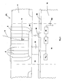
- Figure 1 illustrates schematically the architecture of a detector diode 2 having as a conversion layer a doped semiconductor p + , n + , n ++ trespassing section 4.
- the material choosen for the photodetector diode 2 depends on the desired bandgap energy required to generate a sufficient number of electron hole pairs. Suitable materials are undoped amorphous silicon having band gap of 1.12 eV and a bundle of IV-IV compounds and III-V compounds (indium and gallium salts, like gallium arsenide or indium antimonide).
- An incident particle and/or photon 6 is at least partially absorbed (with respect to its initial energy) in this conversion layer 4. At least almost the complete absorbed energy of the incident particle and/or photon 6 causes in the doped semiconductor p + , n + , n ++ trespassing section 4 a respective number of electron hole pairs 10 in a distinct detector diode 2. In the drawings, this number of electron hole pairs is exemplarily shown by a few electron-hole pairs 10 being divided by the electrical field generated by a source of bias potential 12 via interface 8 and 20.
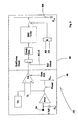
- FIG. 1 Figure 3 now depicts a schematic view on the electronic architecture of a readout unit cell circuitry 44 disposed in the eletronic circuitry layer 16 as capable for use with the two-dimensional pixel detector 14.
- the readout unit cell circuitry 44 can be divided into an analog block 46 and a digital block 48.
- the analog block 46 starts with the bump pad 24 (interface) connected to an input terminal of a charge sensitive amplifier Amp.
- a source of calibration voltage U Cal is connected via a capacitor C to the input terminal of the amplifier Amp, too.
- the capacity of the capacitor has been chosen to a comparably tiny capacity of about only 1.7 fF allowing to be sensitive enough that the photo-electrons can change the voltage over the capacitor C to an extend that this difference can be significantly amplified by the amplifier Amp hereinafter referred to as first output voltage signal.
- This first output voltage signal is led to one of the two input terminals of a comparator amplifier CA which is additionally connected to a source of a threshold voltage supply U T .
- the other input terminal of the comparator amplifier CA is additionally connected to a source of threshold voltage correction supply TC.
- This source of threshold voltage correction supply TC allows to bias the input terminals of the comparator amplifier CA. According to the predetermined bias, of the input terminals of the comparator amplifier CA even the first output voltage signal from the CS amplifier Amp that represents a fractional part of the charge of the generated photo-electron hole pairs only can be further processed and is therefore not lost for the successive data processing and evaluating.
- This electronic readout equipment 44 enables the detection of fractions of the full charge of the photo-electron hole pairs 10 generated by an incident particle and/or photon what may occur when the photo-electron hole pairs 10 are generated in the twilight zone located between two adjacent photodetector diodes 2.
- the source of threshold voltage correction supply TC can be adjusted up to a level defined by one half of the full charge of the photo-electron hole pairs 10 generated in total by an incident x-ray photon 6. Consequentially, the distribution of the charge of the photo-electrons to adjacent photodetector diodes 2 can be further processed.
- a downstream data processing unit is now enabled to perform a differential evaluation of the digital output voltage signals of the comparators having its origin from the photo-electrons in adjacent photodetector diodes 2, whereby these photo-electrons have been generated by the same x-ray photon.
- the fundamental unit of the pixel detector 14 is therefore the combined module, containing a single fully-depleted monolithic silicon sensor 80 x 36 mm 2 x 300 ⁇ m thick, bump-bonded to a 2 x 8 array of readout unit cells 14 using 17 ⁇ m diameter indium balls 22.
- the readout unit cells 18, fabricated on 15 cm wafers in the DMILL radiation tolerant CMOS process, can be arranged in a typical example in an embodiment giving 10 x 20 mm 2 of detector area containing a 44 x 78 array of 217 x 217 ⁇ m 2 pixels. This embodiment is realized in the electronic circuitry layer 16, in which the readunit unit cells 18 are embedded.
- the pixel detector/sensor is continuous, too, and has no dead area. Double-size pixels are used at the chip boundaries to span the gap between readout unit cells 18.
- the pixel detector 14 can be operated at room temperature. Alternatively, it can be water cooled because each module dissipates about 10 W.
- each pixel contains a charge-sensitive preamplifier Amp and shaper (comparator CA), a discriminator, and a 15-bit pseudo-random counter SRC.
- the amplifier noise is 75 e - , which permits single conversion electron counting.
- Each pixel is xy-addressable via a multiplexing means and comprises a 4-bit threshold trim adjustment. Two modes are defined: The counting mode, in which all pixels are individually counting the generated load of electron hole pairs; and the readout mode in which the stored data may be accessed.
- the electronic circuitry layer 16 comprises a plurality of cell testing traces 28 (only one of those is shown in Figure 4 ).
- a cell testing traces 28 is provided in the electronic circuitry layer 16.
- the cell testing traces 28 is disposed in order to allow an electric AC signal to crosstalk into the diode output interface 20.
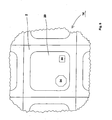
- the cell testing trace 28 may be diposed underneath the surface of the electronic circuitry layer 16. and may comprise a crosstalk section 30 which distinguishes over the other parts of the cell testing traces 28 insofar as to allow the crosstalk of the AC testing signal into the diode output interface 20.
- the cell testing traces 28 enlarge in the electronic circuitry layer 16 being aligned with an electric shielding except for the crosstalk section 30 that remains unshielded and, therefore, leads to the desired leakage/crosstalk properties.
- the cell testing trace 28 is disposed deeper in the electronic circuitry layer 16 and only its crosstalk section 30 extends along the surface in alignment with the diode output interface 20 or a section thereof.
- the data processing means For testing a distinct pixel, the data processing means generates an AC cell testing signal that is directed via a suitable multiplexing means to the cell testing trace 28 of this distinct predetermined readout unit cell 18.
- the AC cell testing signal even flows through the crosstalk section 30 and is enabled by the design of the crosstalk section 30 to couple capacitively into the diode output interface 20.
- the crosstalk signal itself is amplified by the high gain low noise amplifier AMP in the analog part 46 of the readout unit cell 18.
- For the further signal processing applies the same as for a signal generated by the conversion of an incident particle and/or photon.
- the frequency composition and/or the amplitude of the AC cell testing signal can be selected in a broad range depending on the design of at leat one of the gap 32 between the semiconductor layer 4 and the electronic circuitry layer 16.
- the gap 32 is an air gap.
- this gap 32 may be filled with a dielectric, such as a ceramic insulator.
Landscapes
- Physics & Mathematics (AREA)
- Health & Medical Sciences (AREA)
- Life Sciences & Earth Sciences (AREA)
- General Physics & Mathematics (AREA)
- High Energy & Nuclear Physics (AREA)
- Molecular Biology (AREA)
- Spectroscopy & Molecular Physics (AREA)
- Measurement Of Radiation (AREA)
Claims (9)
- Détecteur ( 14 ) de pixel pour une particule et/ou un rayonnement ( 6 ) de photon, comprenant :a) une couche ( 4 ) de conversion comprenant une matière de conversion sensible à la particule et/ou au rayonnement ( 6 ) de photon ;b) une matrice NxM de diodes ( 2 ) formant détecteurs disposée dans la couche ( 4 ) de conversion ; chacune des diodes ( 2 ) formant détecteurs ayant une interface ( 8 ) de potentiel de polarisation et une interface ( 20 ) de sortie de diode ;c) une couche ( 16 ) de circuit électronique comprenant une matrice NxM de cellules ( 18 ) unitaires de lecture à grand gain et à faible bruit, une cellule ( 18 ) unitaire de lecture pour chaque diode ( 2 ) formant détecteur et une pluralité de pistes de circuit ;d) la pluralité de pistes de circuit comprend une pluralité de pistes ( 28 ) de test de cellule pour au moins une partie des cellules ( 18 ) unitaires de lecture ;e) des moyens de production d'un signal de test et d'envoi de ce signal aux pistes ( 28 ) de test de cellules ( 18 ) unitaires de lecture distinctes déterminées à l'avance ;f) les pistes ( 28 ) de test de cellule sont disposées, au moins en partie, par rapport aux diodes ( 2 ) formant détecteurs, de manière à permettre à un signal de test sur une piste ( 18 ) distincte de test de cellule de venir en diaphonie dans la diode ( 2 ) respective formant détecteur.
- Détecteur ( 14 ) de pixel suivant la revendication 1, caractérisé en ce que
les pistes ( 28 ) de test de cellule ayant une section ( 30 ) de diaphonie, chaque section ( 30 ) de diaphonie est disposée, au moins en partie, à la surface de la couche ( 16 ) de circuit électronique. - Détecteur ( 14 ) de pixel suivant la revendication 1 ou 2, caractérisé en ce que
la section ( 30 ) de diaphonie est disposée, au moins en partie, à l'opposé de l'interface ( 20 ) de sortie de la diode. - Détecteur ( 14 ) de pixel suivant l'une quelconque des revendications précédentes, caractérisé en ce que
le signal de test est fourni par un moyen de traitement de données ; le moyen de traitement de données étant relié par un moyen de multiplexeur à la matrice de cellules ( 18 ) unitaires de lecture en permettant de commander chaque piste ( 28 ) de test de cellule de la cellule ( 18 ) unitaires de lecture respective. - Détecteur ( 14 ) de pixel suivant la revendication 4, caractérisé en ce que
les moyens de traitement de données commandent, par l'intermédiaire des moyens de multiplexage, une ou plusieurs des fonctions suivantes :a) programmation de la cellule ( 18 ) unitaire de lecture ;b) lecture des données dans la cellule ( 18 ) unitaire de lecture ;c) étalonnage de la cellule ( 18 ) unitaire de lecture, de préférence un moyen ( Amp, CA ) amplificateur de tension à grand gain ;d) analyse du signal analogique dans le moyen ( Amp, CA ) amplificateur de tension à grand gain à des fins de diagnostic ; ete) fixation d'un seuil inférieur et/ou d'un seuil supérieur d'une unité de seuil comprise dans chaque cellule ( 18 ) unitaire de lecture. - Détecteur ( 14 ) de pixel suivant l'une quelconque des revendications précédentes, caractérisé en ce que la couche ( 4 ) de conversion est une couche semiconductrice.
- Détecteur ( 14 ) de pixel suivant l'une quelconque des revendications précédentes, caractérisé en ce que la diaphonie est obtenue par couplage capacitif.
- Détecteur ( 14 ) de pixel suivant la revendication 7, caractérisé en ce que
un intervalle ( 32 ) d'air est disposé entre la section ( 30 ) de diaphonie des pistes ( 28 ) de test de cellule et la diode ( 2 ) formant détecteur, de préférence l'interface ( 20 ) de sortie de la diode ( 2 ) formant détecteur. - Procédé de test d'un détecteur ( 14 ) de pixel ayant une pluralité de diodes ( 2 ) formant détecteurs disposées dans une couche ( 4 ) de conversion et une pluralité de cellules ( 18 ) unitaires de lecture disposées dans une couche ( 16 ) de circuit électronique comprenant :a) produire un signal de test de cellule ;b) envoyer ce signal de test de cellule à une piste ( 28 ) de test de cellule disposée dans la couche ( 16 ) de circuit électronique ;c) permettre une diaphonie du signal de test de cellule dans la diode ( 2 ) respective formant détecteur afin de produire un signal de diaphonie ;d) amplifier le signal de diaphonie obtenu de la diode ( 2 ) respective formant détecteur dans la cellule ( 18 ) unitaire de lecture ; ete) évaluer le signal amplifié de diaphonie en réaction au signal de test de cellule.
Priority Applications (1)
| Application Number | Priority Date | Filing Date | Title |
|---|---|---|---|
| EP20040026776 EP1538460B1 (fr) | 2003-12-04 | 2004-11-11 | Détecteur à pixels pour des particules et / ou des photons ayant des facultés de test améliorées et procédé pour tester un détecteur à pixels |
Applications Claiming Priority (3)
| Application Number | Priority Date | Filing Date | Title |
|---|---|---|---|
| EP03027914 | 2003-12-04 | ||
| EP03027914 | 2003-12-04 | ||
| EP20040026776 EP1538460B1 (fr) | 2003-12-04 | 2004-11-11 | Détecteur à pixels pour des particules et / ou des photons ayant des facultés de test améliorées et procédé pour tester un détecteur à pixels |
Publications (2)
| Publication Number | Publication Date |
|---|---|
| EP1538460A1 EP1538460A1 (fr) | 2005-06-08 |
| EP1538460B1 true EP1538460B1 (fr) | 2012-12-26 |
Family
ID=34466340
Family Applications (1)
| Application Number | Title | Priority Date | Filing Date |
|---|---|---|---|
| EP20040026776 Expired - Lifetime EP1538460B1 (fr) | 2003-12-04 | 2004-11-11 | Détecteur à pixels pour des particules et / ou des photons ayant des facultés de test améliorées et procédé pour tester un détecteur à pixels |
Country Status (1)
| Country | Link |
|---|---|
| EP (1) | EP1538460B1 (fr) |
Families Citing this family (1)
| Publication number | Priority date | Publication date | Assignee | Title |
|---|---|---|---|---|
| CN113433584B (zh) * | 2021-06-28 | 2022-11-04 | 哈尔滨工业大学 | 可兼容电子收集和空穴收集的像素探测器中的像素电路 |
Family Cites Families (4)
| Publication number | Priority date | Publication date | Assignee | Title |
|---|---|---|---|---|
| FR2286393A1 (fr) * | 1974-09-27 | 1976-04-23 | Labo Electronique Physique | Systeme automatique de reetalonnage permanent pour camera a scintillation |
| US4687622A (en) * | 1985-10-29 | 1987-08-18 | Irt Corporation | Nuclear event detector |
| EP0523784A1 (fr) * | 1991-07-15 | 1993-01-20 | Philips Electronics Uk Limited | Détecteur produisant des images et méthode pour sa fabrication |
| US6404851B1 (en) * | 2000-03-30 | 2002-06-11 | General Electric Company | Method and apparatus for automatic exposure control using localized capacitive coupling in a matrix-addressed imaging panel |
-
2004
- 2004-11-11 EP EP20040026776 patent/EP1538460B1/fr not_active Expired - Lifetime
Also Published As
| Publication number | Publication date |
|---|---|
| EP1538460A1 (fr) | 2005-06-08 |
Similar Documents
| Publication | Publication Date | Title |
|---|---|---|
| EP1581971B1 (fr) | Dispositif d'imagerie a comptage de photons | |
| EP2130063A1 (fr) | Procédé, appareil et programme informatique pour mesurer la dose, le débit de dose, ou la composition d'un rayonnement | |
| JP2005539232A (ja) | 複数の検出器ユニットを有するx線検出器 | |
| US7138632B2 (en) | Radiation detector | |
| GB2265753A (en) | Ionizing ray microimaging device | |
| JP4934826B2 (ja) | 放射線画像検出モジュールおよび放射線画像検出装置 | |
| Parker et al. | 3DX: An X-ray pixel array detector with active edges | |
| McConnell et al. | Three-dimensional imaging and detection efficiency performance of orthogonal coplanar CZT strip detectors | |
| Hong et al. | Building large area CZT imaging detectors for a wide-field hard X-ray telescope—ProtoEXIST1 | |
| EP1538460B1 (fr) | Détecteur à pixels pour des particules et / ou des photons ayant des facultés de test améliorées et procédé pour tester un détecteur à pixels | |
| KR20230136198A (ko) | 방사선 촬상 장치 | |
| EP3794380B1 (fr) | Unité de capteur, détecteur de rayonnement et procédé de fabrication d'une unité de capteur | |
| US7042008B2 (en) | Image sensor and method of manufacturing the same | |
| JP2015141037A (ja) | 放射線検出器 | |
| Tumer et al. | Preliminary test results of pixel detectors developed for All-sky X-ray and Gamma-ray Astronomy Monitor (AXGAM) | |
| Tojo et al. | Development of a novel silicon stripixel detector for RHIC-PHENIX detector upgrade | |
| CN119563125B (zh) | 具有突出的集成电路芯片的侧入射图像传感器 | |
| Allaire et al. | First light of MC2-1K, a 250 μm pixel pitch CdTe imaging spectrometer for hard X-ray astronomy | |
| WO2023123301A1 (fr) | Systèmes d'imagerie avec capteurs d'image rotatifs | |
| Wentink et al. | Charge Injection Device (CID) technology—A solution for photon and particle imaging applications | |
| JP2015125063A (ja) | 放射線検出器 | |
| Delpierre et al. | Development of silicon micropattern (pixel) detectors | |
| CZ36509U1 (cs) | Detekční modul detektoru neutronů | |
| Hatzistratis et al. | CMOS Pixel Spectroscopic Circuits for Cd (Zn) Te Gamma Ray Imagers | |
| CN118318311A (zh) | 包含钙钛矿的辐射检测器 |
Legal Events
| Date | Code | Title | Description |
|---|---|---|---|
| PUAI | Public reference made under article 153(3) epc to a published international application that has entered the european phase |
Free format text: ORIGINAL CODE: 0009012 |
|
| AK | Designated contracting states |
Kind code of ref document: A1 Designated state(s): AT BE BG CH CY CZ DE DK EE ES FI FR GB GR HU IE IS IT LI LU MC NL PL PT RO SE SI SK TR |
|
| AX | Request for extension of the european patent |
Extension state: AL HR LT LV MK YU |
|
| 17P | Request for examination filed |
Effective date: 20051010 |
|
| AKX | Designation fees paid |
Designated state(s): AT BE BG CH CY CZ DE DK EE ES FI FR GB GR HU IE IS IT LI LU MC NL PL PT RO SE SI SK TR |
|
| 17Q | First examination report despatched |
Effective date: 20110516 |
|
| RIC1 | Information provided on ipc code assigned before grant |
Ipc: G01T 1/24 20060101AFI20120418BHEP Ipc: G01T 1/17 20060101ALI20120418BHEP Ipc: G01T 1/29 20060101ALI20120418BHEP Ipc: G01T 3/08 20060101ALI20120418BHEP |
|
| GRAP | Despatch of communication of intention to grant a patent |
Free format text: ORIGINAL CODE: EPIDOSNIGR1 |
|
| GRAS | Grant fee paid |
Free format text: ORIGINAL CODE: EPIDOSNIGR3 |
|
| RAP1 | Party data changed (applicant data changed or rights of an application transferred) |
Owner name: DECTRIS AG |
|
| GRAA | (expected) grant |
Free format text: ORIGINAL CODE: 0009210 |
|
| AK | Designated contracting states |
Kind code of ref document: B1 Designated state(s): AT BE BG CH CY CZ DE DK EE ES FI FR GB GR HU IE IS IT LI LU MC NL PL PT RO SE SI SK TR |
|
| REG | Reference to a national code |
Ref country code: GB Ref legal event code: FG4D |
|
| REG | Reference to a national code |
Ref country code: CH Ref legal event code: EP |
|
| REG | Reference to a national code |
Ref country code: AT Ref legal event code: REF Ref document number: 590759 Country of ref document: AT Kind code of ref document: T Effective date: 20130115 |
|
| REG | Reference to a national code |
Ref country code: DE Ref legal event code: R096 Ref document number: 602004040513 Country of ref document: DE Effective date: 20130307 |
|
| PG25 | Lapsed in a contracting state [announced via postgrant information from national office to epo] |
Ref country code: FI Free format text: LAPSE BECAUSE OF FAILURE TO SUBMIT A TRANSLATION OF THE DESCRIPTION OR TO PAY THE FEE WITHIN THE PRESCRIBED TIME-LIMIT Effective date: 20121226 Ref country code: SE Free format text: LAPSE BECAUSE OF FAILURE TO SUBMIT A TRANSLATION OF THE DESCRIPTION OR TO PAY THE FEE WITHIN THE PRESCRIBED TIME-LIMIT Effective date: 20121226 |
|
| REG | Reference to a national code |
Ref country code: AT Ref legal event code: MK05 Ref document number: 590759 Country of ref document: AT Kind code of ref document: T Effective date: 20121226 |
|
| REG | Reference to a national code |
Ref country code: NL Ref legal event code: VDEP Effective date: 20121226 |
|
| PG25 | Lapsed in a contracting state [announced via postgrant information from national office to epo] |
Ref country code: SI Free format text: LAPSE BECAUSE OF FAILURE TO SUBMIT A TRANSLATION OF THE DESCRIPTION OR TO PAY THE FEE WITHIN THE PRESCRIBED TIME-LIMIT Effective date: 20121226 Ref country code: GR Free format text: LAPSE BECAUSE OF FAILURE TO SUBMIT A TRANSLATION OF THE DESCRIPTION OR TO PAY THE FEE WITHIN THE PRESCRIBED TIME-LIMIT Effective date: 20130327 |
|
| PG25 | Lapsed in a contracting state [announced via postgrant information from national office to epo] |
Ref country code: SK Free format text: LAPSE BECAUSE OF FAILURE TO SUBMIT A TRANSLATION OF THE DESCRIPTION OR TO PAY THE FEE WITHIN THE PRESCRIBED TIME-LIMIT Effective date: 20121226 Ref country code: BG Free format text: LAPSE BECAUSE OF FAILURE TO SUBMIT A TRANSLATION OF THE DESCRIPTION OR TO PAY THE FEE WITHIN THE PRESCRIBED TIME-LIMIT Effective date: 20130326 Ref country code: CY Free format text: LAPSE BECAUSE OF FAILURE TO SUBMIT A TRANSLATION OF THE DESCRIPTION OR TO PAY THE FEE WITHIN THE PRESCRIBED TIME-LIMIT Effective date: 20121226 Ref country code: ES Free format text: LAPSE BECAUSE OF FAILURE TO SUBMIT A TRANSLATION OF THE DESCRIPTION OR TO PAY THE FEE WITHIN THE PRESCRIBED TIME-LIMIT Effective date: 20130406 Ref country code: IS Free format text: LAPSE BECAUSE OF FAILURE TO SUBMIT A TRANSLATION OF THE DESCRIPTION OR TO PAY THE FEE WITHIN THE PRESCRIBED TIME-LIMIT Effective date: 20130426 Ref country code: BE Free format text: LAPSE BECAUSE OF FAILURE TO SUBMIT A TRANSLATION OF THE DESCRIPTION OR TO PAY THE FEE WITHIN THE PRESCRIBED TIME-LIMIT Effective date: 20121226 Ref country code: EE Free format text: LAPSE BECAUSE OF FAILURE TO SUBMIT A TRANSLATION OF THE DESCRIPTION OR TO PAY THE FEE WITHIN THE PRESCRIBED TIME-LIMIT Effective date: 20121226 Ref country code: CZ Free format text: LAPSE BECAUSE OF FAILURE TO SUBMIT A TRANSLATION OF THE DESCRIPTION OR TO PAY THE FEE WITHIN THE PRESCRIBED TIME-LIMIT Effective date: 20121226 Ref country code: AT Free format text: LAPSE BECAUSE OF FAILURE TO SUBMIT A TRANSLATION OF THE DESCRIPTION OR TO PAY THE FEE WITHIN THE PRESCRIBED TIME-LIMIT Effective date: 20121226 |
|
| PG25 | Lapsed in a contracting state [announced via postgrant information from national office to epo] |
Ref country code: PT Free format text: LAPSE BECAUSE OF FAILURE TO SUBMIT A TRANSLATION OF THE DESCRIPTION OR TO PAY THE FEE WITHIN THE PRESCRIBED TIME-LIMIT Effective date: 20130426 Ref country code: RO Free format text: LAPSE BECAUSE OF FAILURE TO SUBMIT A TRANSLATION OF THE DESCRIPTION OR TO PAY THE FEE WITHIN THE PRESCRIBED TIME-LIMIT Effective date: 20121226 Ref country code: NL Free format text: LAPSE BECAUSE OF FAILURE TO SUBMIT A TRANSLATION OF THE DESCRIPTION OR TO PAY THE FEE WITHIN THE PRESCRIBED TIME-LIMIT Effective date: 20121226 Ref country code: PL Free format text: LAPSE BECAUSE OF FAILURE TO SUBMIT A TRANSLATION OF THE DESCRIPTION OR TO PAY THE FEE WITHIN THE PRESCRIBED TIME-LIMIT Effective date: 20121226 |
|
| PG25 | Lapsed in a contracting state [announced via postgrant information from national office to epo] |
Ref country code: DK Free format text: LAPSE BECAUSE OF FAILURE TO SUBMIT A TRANSLATION OF THE DESCRIPTION OR TO PAY THE FEE WITHIN THE PRESCRIBED TIME-LIMIT Effective date: 20121226 |
|
| PLBE | No opposition filed within time limit |
Free format text: ORIGINAL CODE: 0009261 |
|
| STAA | Information on the status of an ep patent application or granted ep patent |
Free format text: STATUS: NO OPPOSITION FILED WITHIN TIME LIMIT |
|
| 26N | No opposition filed |
Effective date: 20130927 |
|
| PG25 | Lapsed in a contracting state [announced via postgrant information from national office to epo] |
Ref country code: IT Free format text: LAPSE BECAUSE OF FAILURE TO SUBMIT A TRANSLATION OF THE DESCRIPTION OR TO PAY THE FEE WITHIN THE PRESCRIBED TIME-LIMIT Effective date: 20121226 |
|
| REG | Reference to a national code |
Ref country code: DE Ref legal event code: R097 Ref document number: 602004040513 Country of ref document: DE Effective date: 20130927 |
|
| REG | Reference to a national code |
Ref country code: CH Ref legal event code: PL |
|
| PG25 | Lapsed in a contracting state [announced via postgrant information from national office to epo] |
Ref country code: CH Free format text: LAPSE BECAUSE OF NON-PAYMENT OF DUE FEES Effective date: 20131130 Ref country code: LI Free format text: LAPSE BECAUSE OF NON-PAYMENT OF DUE FEES Effective date: 20131130 Ref country code: MC Free format text: LAPSE BECAUSE OF FAILURE TO SUBMIT A TRANSLATION OF THE DESCRIPTION OR TO PAY THE FEE WITHIN THE PRESCRIBED TIME-LIMIT Effective date: 20121226 |
|
| REG | Reference to a national code |
Ref country code: IE Ref legal event code: MM4A |
|
| PG25 | Lapsed in a contracting state [announced via postgrant information from national office to epo] |
Ref country code: DE Free format text: LAPSE BECAUSE OF NON-PAYMENT OF DUE FEES Effective date: 20140603 |
|
| REG | Reference to a national code |
Ref country code: DE Ref legal event code: R119 Ref document number: 602004040513 Country of ref document: DE Effective date: 20140603 |
|
| PG25 | Lapsed in a contracting state [announced via postgrant information from national office to epo] |
Ref country code: IE Free format text: LAPSE BECAUSE OF NON-PAYMENT OF DUE FEES Effective date: 20131111 |
|
| PG25 | Lapsed in a contracting state [announced via postgrant information from national office to epo] |
Ref country code: TR Free format text: LAPSE BECAUSE OF FAILURE TO SUBMIT A TRANSLATION OF THE DESCRIPTION OR TO PAY THE FEE WITHIN THE PRESCRIBED TIME-LIMIT Effective date: 20121226 |
|
| PG25 | Lapsed in a contracting state [announced via postgrant information from national office to epo] |
Ref country code: LU Free format text: LAPSE BECAUSE OF NON-PAYMENT OF DUE FEES Effective date: 20131111 Ref country code: HU Free format text: LAPSE BECAUSE OF FAILURE TO SUBMIT A TRANSLATION OF THE DESCRIPTION OR TO PAY THE FEE WITHIN THE PRESCRIBED TIME-LIMIT; INVALID AB INITIO Effective date: 20041111 |
|
| REG | Reference to a national code |
Ref country code: FR Ref legal event code: PLFP Year of fee payment: 12 |
|
| REG | Reference to a national code |
Ref country code: FR Ref legal event code: CA Effective date: 20160301 |
|
| REG | Reference to a national code |
Ref country code: FR Ref legal event code: PLFP Year of fee payment: 13 |
|
| PGFP | Annual fee paid to national office [announced via postgrant information from national office to epo] |
Ref country code: FR Payment date: 20161128 Year of fee payment: 13 Ref country code: GB Payment date: 20161130 Year of fee payment: 13 |
|
| GBPC | Gb: european patent ceased through non-payment of renewal fee |
Effective date: 20171111 |
|
| REG | Reference to a national code |
Ref country code: FR Ref legal event code: ST Effective date: 20180731 |
|
| PG25 | Lapsed in a contracting state [announced via postgrant information from national office to epo] |
Ref country code: FR Free format text: LAPSE BECAUSE OF NON-PAYMENT OF DUE FEES Effective date: 20171130 |
|
| PG25 | Lapsed in a contracting state [announced via postgrant information from national office to epo] |
Ref country code: GB Free format text: LAPSE BECAUSE OF NON-PAYMENT OF DUE FEES Effective date: 20171111 |