EP1538525A1 - Calcul simultané de ECC pendant la lecture ou la programmation d'une mémoire flash - Google Patents
Calcul simultané de ECC pendant la lecture ou la programmation d'une mémoire flash Download PDFInfo
- Publication number
- EP1538525A1 EP1538525A1 EP03293051A EP03293051A EP1538525A1 EP 1538525 A1 EP1538525 A1 EP 1538525A1 EP 03293051 A EP03293051 A EP 03293051A EP 03293051 A EP03293051 A EP 03293051A EP 1538525 A1 EP1538525 A1 EP 1538525A1
- Authority
- EP
- European Patent Office
- Prior art keywords
- ecc
- flash memory
- data
- computation
- programming
- Prior art date
- Legal status (The legal status is an assumption and is not a legal conclusion. Google has not performed a legal analysis and makes no representation as to the accuracy of the status listed.)
- Withdrawn
Links
Images


Classifications
-
- G—PHYSICS
- G11—INFORMATION STORAGE
- G11C—STATIC STORES
- G11C16/00—Erasable programmable read-only memories
- G11C16/02—Erasable programmable read-only memories electrically programmable
- G11C16/06—Auxiliary circuits, e.g. for writing into memory
- G11C16/10—Programming or data input circuits
Definitions
- the present invention relates to Error Correction Code (ECC) computation, and, more particularly, to an apparatus and method for streamlining ECC computation.
- ECC Error Correction Code
- ECC Error Correction Code
- a method of streamlining ECC computation comprising: computing ECC concurrently while either reading data from Flash memory or programming data to or from Flash memory, so that a block of data does not have to be saved in memory before the ECC computation can be started.
- the block or data is 256 bytes or 512 bytes in size.
- the method further comprises: when the ECC computation for the block of data is completed, saving the ECC for the block of data in a first ECC register; and moving an ECC pointer to the next ECC register so that when the ECC for the next block of data is computed, it is saved immediately.
- the ECC computation for the block of data is completed, saving the ECC for the block of data in a first ECC register; and moving an ECC pointer to the next ECC register so that when the ECC for the next block of data is computed, it is saved immediately.
- the block of data is 256 bytes in size, and for a 2 Kbyte page with a spare area of 64 bytes of Flash memory, 9 registers are used.
- the invention avoids any penalty in performance and further provides an improvement in performance by conducting ECC computation concurrently with reading or programming a Flash memory. Further advantageously, a full page of Flash memory can be read or program without having to stop and wait for ECC computation. Also advantageously, no time is lost by automatically switching to a next register when one ECC computation on a block of data is complete.
- the present invention provides a method and apparatus for streamlining Error Correction Code (ECC) computation by conducting ECC computation concurrently with either a data read from a flash memory or a program to the flash memory.
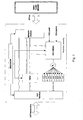
- Figure 1 is a diagram showing the principle of a NAND Flash Controller with onboard ECC engine in accordance with a preferred embodiment.
- FIGS 2a and 2b are block diagrams showing the steps involved in the method of streamlining ECC computation according to the preferred embodiment.
- the steps involved in conducting ECC computation concurrently with a data read will be described.
- the type of ECC is selected: 256 bytes or 512 bytes.
- a data read command is sent to the NAND Flash memory.
- a start_address is sent to the NAND Flash memory, and either DMA or HOST access is chosen for data.
- ECC is computed concurrently with the data being read, as is more fully explained below with reference to Figure 3.
- the ECC registers are read and are compared with the ones in the spare area in the NAND Flash memory, and correction of errors are eventually carried out using software.
- Figure 2b shows a similar process for conducting ECC computation while programming Flash memory.
- the type of ECC is selected: 256 bytes or 512 bytes.
- a program command is sent to the NAND Flash memory.
- a start_address is sent to the NAND Flash memory, and either DMA or HOST access is chosen for data.
- ECC is computed concurrently with the data being sent, as is more fully explained below with reference to Figure 3.
- the ECC registers are read and are saved in the spare area in the NAND Flash memory.
- ECC computation is carried out concurrently with either a data read from the NAND Flash memory or program to the NAND Flash memory, so that a block of 256 or 512 bytes do not have to be saved in memory before the ECC checking can be started. Hence there is no penalty in performance.
- the invention provides an improvement in performance because, as soon as a block of 256 or 512 bytes of data (which is selectable) has its ECC ready, the ECC is saved in the first ECC register and the ECC pointer moves to the next ECC register so that when the next block of data has its ECC ready, it is automatically saved, the ECC pointer moves to next ECC register, and so the process continues. There are enough registers to protect a page. For a 2Kbyte page + spare area (64 bytes) of NAND Flash memory, and for an ECC computation on 256 bytes, 9 registers are necessary.
- a full page of NAND Flash memory can be read or program without having to stop and wait for ECC computation.
- This method is particularly efficient when a DMA engine reads data from Flash memory or programs data to Flash memory, since the host processor does not have to stop every block of 256 or 512 bytes (depending on the chosen ECC) to dump the ECC registers.
- the software detects an error by comparaing the calculated ECC to the previous one which was done when a page was programmed.
- This technique works whatever the data size (8 bits or 16 bits NAND Flash memory).
- a futher advantage of the technique is that no external memory is needed except the one needed to save the data from the NAND Flash.
Landscapes
- Techniques For Improving Reliability Of Storages (AREA)
Priority Applications (2)
| Application Number | Priority Date | Filing Date | Title |
|---|---|---|---|
| EP03293051A EP1538525A1 (fr) | 2003-12-04 | 2003-12-04 | Calcul simultané de ECC pendant la lecture ou la programmation d'une mémoire flash |
| US10/764,670 US7823044B2 (en) | 2003-12-04 | 2004-01-26 | Method for streamlining error connection code computation while reading or programming a NAND flash memory |
Applications Claiming Priority (1)
| Application Number | Priority Date | Filing Date | Title |
|---|---|---|---|
| EP03293051A EP1538525A1 (fr) | 2003-12-04 | 2003-12-04 | Calcul simultané de ECC pendant la lecture ou la programmation d'une mémoire flash |
Publications (1)
| Publication Number | Publication Date |
|---|---|
| EP1538525A1 true EP1538525A1 (fr) | 2005-06-08 |
Family
ID=34443124
Family Applications (1)
| Application Number | Title | Priority Date | Filing Date |
|---|---|---|---|
| EP03293051A Withdrawn EP1538525A1 (fr) | 2003-12-04 | 2003-12-04 | Calcul simultané de ECC pendant la lecture ou la programmation d'une mémoire flash |
Country Status (2)
| Country | Link |
|---|---|
| US (1) | US7823044B2 (fr) |
| EP (1) | EP1538525A1 (fr) |
Cited By (2)
| Publication number | Priority date | Publication date | Assignee | Title |
|---|---|---|---|---|
| US20150378823A1 (en) * | 2013-03-25 | 2015-12-31 | Hewlett-Packard Development Company, L.P. | Memory device having error correction logic |
| EP2972916A4 (fr) * | 2013-03-13 | 2017-04-12 | Intel Corporation | Gestion du temps de latence mémoire |
Families Citing this family (26)
| Publication number | Priority date | Publication date | Assignee | Title |
|---|---|---|---|---|
| US7644239B2 (en) | 2004-05-03 | 2010-01-05 | Microsoft Corporation | Non-volatile memory cache performance improvement |
| US7490197B2 (en) | 2004-10-21 | 2009-02-10 | Microsoft Corporation | Using external memory devices to improve system performance |
| US8291295B2 (en) * | 2005-09-26 | 2012-10-16 | Sandisk Il Ltd. | NAND flash memory controller exporting a NAND interface |
| US8914557B2 (en) | 2005-12-16 | 2014-12-16 | Microsoft Corporation | Optimizing write and wear performance for a memory |
| US7304893B1 (en) | 2006-06-30 | 2007-12-04 | Sandisk Corporation | Method of partial page fail bit detection in flash memory devices |
| US7355892B2 (en) * | 2006-06-30 | 2008-04-08 | Sandisk Corporation | Partial page fail bit detection in flash memory devices |
| JP2008090433A (ja) * | 2006-09-29 | 2008-04-17 | Toshiba Corp | メモリコントローラ、メモリシステム及びデータ転送方法 |
| US7440319B2 (en) * | 2006-11-27 | 2008-10-21 | Sandisk Corporation | Apparatus with segmented bitscan for verification of programming |
| US7545681B2 (en) * | 2006-11-27 | 2009-06-09 | Sandisk Corporation | Segmented bitscan for verification of programming |
| US8055982B2 (en) * | 2007-02-21 | 2011-11-08 | Sigmatel, Inc. | Error correction system and method |
| US9471418B2 (en) | 2007-06-19 | 2016-10-18 | Samsung Electronics Co., Ltd. | Memory system that detects bit errors due to read disturbance and methods thereof |
| KR100882841B1 (ko) * | 2007-06-19 | 2009-02-10 | 삼성전자주식회사 | 읽기 디스터번스로 인한 비트 에러를 검출할 수 있는메모리 시스템 및 그것의 읽기 방법 |
| KR101433861B1 (ko) * | 2007-10-22 | 2014-08-27 | 삼성전자주식회사 | 메모리 시스템 및 그 구동방법 |
| US8631203B2 (en) | 2007-12-10 | 2014-01-14 | Microsoft Corporation | Management of external memory functioning as virtual cache |
| US8032707B2 (en) | 2008-09-15 | 2011-10-04 | Microsoft Corporation | Managing cache data and metadata |
| US9032151B2 (en) | 2008-09-15 | 2015-05-12 | Microsoft Technology Licensing, Llc | Method and system for ensuring reliability of cache data and metadata subsequent to a reboot |
| US7953774B2 (en) | 2008-09-19 | 2011-05-31 | Microsoft Corporation | Aggregation of write traffic to a data store |
| US8307258B2 (en) | 2009-05-18 | 2012-11-06 | Fusion-10, Inc | Apparatus, system, and method for reconfiguring an array to operate with less storage elements |
| US8054691B2 (en) | 2009-06-26 | 2011-11-08 | Sandisk Technologies Inc. | Detecting the completion of programming for non-volatile storage |
| US20110041005A1 (en) * | 2009-08-11 | 2011-02-17 | Selinger Robert D | Controller and Method for Providing Read Status and Spare Block Management Information in a Flash Memory System |
| KR101617641B1 (ko) * | 2009-08-27 | 2016-05-03 | 삼성전자주식회사 | 비휘발성 메모리 장치, 그것을 포함한 메모리 시스템, 및 그것의 프로그램 방법 |
| US9009570B2 (en) | 2012-06-07 | 2015-04-14 | Micron Technology, Inc. | Integrity of an address bus |
| US9323608B2 (en) | 2012-06-07 | 2016-04-26 | Micron Technology, Inc. | Integrity of a data bus |
| KR101997794B1 (ko) | 2012-12-11 | 2019-07-09 | 삼성전자주식회사 | 메모리 제어기 및 그것을 포함한 메모리 시스템 |
| US9535785B2 (en) * | 2014-01-17 | 2017-01-03 | Macronix International Co., Ltd. | ECC method for flash memory |
| US9798620B2 (en) | 2014-02-06 | 2017-10-24 | Sandisk Technologies Llc | Systems and methods for non-blocking solid-state memory |
Citations (2)
| Publication number | Priority date | Publication date | Assignee | Title |
|---|---|---|---|---|
| US20010001327A1 (en) * | 1995-07-14 | 2001-05-17 | Takayuki Tamura | External storage device and memory access control method thereof |
| US6510537B1 (en) * | 1998-08-07 | 2003-01-21 | Samsung Electronics Co., Ltd | Semiconductor memory device with an on-chip error correction circuit and a method for correcting a data error therein |
Family Cites Families (12)
| Publication number | Priority date | Publication date | Assignee | Title |
|---|---|---|---|---|
| KR100359414B1 (ko) * | 1996-01-25 | 2003-01-24 | 동경 엘렉트론 디바이스 주식회사 | 데이타독출/기록방법및그를이용한메모리제어장치및시스템 |
| US6018778A (en) * | 1996-05-03 | 2000-01-25 | Netcell Corporation | Disk array controller for reading/writing striped data using a single address counter for synchronously transferring data between data ports and buffer memory |
| US6034891A (en) * | 1997-12-01 | 2000-03-07 | Micron Technology, Inc. | Multi-state flash memory defect management |
| US6594792B1 (en) * | 1999-04-30 | 2003-07-15 | General Electric Company | Modular turbo decoder for expanded code word length |
| JP4282197B2 (ja) * | 2000-01-24 | 2009-06-17 | 株式会社ルネサステクノロジ | 不揮発性半導体記憶装置 |
| US6426893B1 (en) * | 2000-02-17 | 2002-07-30 | Sandisk Corporation | Flash eeprom system with simultaneous multiple data sector programming and storage of physical block characteristics in other designated blocks |
| US6438039B1 (en) * | 2001-07-03 | 2002-08-20 | Macronix International Co., Ltd. | Erasing device and method for flash memory |
| US6883131B2 (en) * | 2001-09-28 | 2005-04-19 | Sun Microsystems, Inc. | XOR processing incorporating error correction code data protection |
| US6683817B2 (en) * | 2002-02-21 | 2004-01-27 | Qualcomm, Incorporated | Direct memory swapping between NAND flash and SRAM with error correction coding |
| JP4205396B2 (ja) * | 2002-10-30 | 2009-01-07 | エルピーダメモリ株式会社 | 半導体集積回路装置 |
| US6906961B2 (en) * | 2003-06-24 | 2005-06-14 | Micron Technology, Inc. | Erase block data splitting |
| US6975140B2 (en) * | 2003-11-26 | 2005-12-13 | International Business Machines Corporation | Adaptive data transmitter having rewriteable non-volatile storage |
-
2003
- 2003-12-04 EP EP03293051A patent/EP1538525A1/fr not_active Withdrawn
-
2004
- 2004-01-26 US US10/764,670 patent/US7823044B2/en not_active Expired - Lifetime
Patent Citations (2)
| Publication number | Priority date | Publication date | Assignee | Title |
|---|---|---|---|---|
| US20010001327A1 (en) * | 1995-07-14 | 2001-05-17 | Takayuki Tamura | External storage device and memory access control method thereof |
| US6510537B1 (en) * | 1998-08-07 | 2003-01-21 | Samsung Electronics Co., Ltd | Semiconductor memory device with an on-chip error correction circuit and a method for correcting a data error therein |
Cited By (6)
| Publication number | Priority date | Publication date | Assignee | Title |
|---|---|---|---|---|
| EP2972916A4 (fr) * | 2013-03-13 | 2017-04-12 | Intel Corporation | Gestion du temps de latence mémoire |
| US9904592B2 (en) | 2013-03-13 | 2018-02-27 | Intel Corporation | Memory latency management |
| US10572339B2 (en) | 2013-03-13 | 2020-02-25 | Intel Corporation | Memory latency management |
| US20150378823A1 (en) * | 2013-03-25 | 2015-12-31 | Hewlett-Packard Development Company, L.P. | Memory device having error correction logic |
| EP2979271A4 (fr) * | 2013-03-25 | 2016-11-30 | Hewlett Packard Entpr Dev Lp | Dispositif de mémoire ayant une logique de correction d'erreur |
| US10417091B2 (en) * | 2013-03-25 | 2019-09-17 | Hewlett Packard Enterprise Development Lp | Memory device having error correction logic |
Also Published As
| Publication number | Publication date |
|---|---|
| US7823044B2 (en) | 2010-10-26 |
| US20050125708A1 (en) | 2005-06-09 |
Similar Documents
| Publication | Publication Date | Title |
|---|---|---|
| EP1538525A1 (fr) | Calcul simultané de ECC pendant la lecture ou la programmation d'une mémoire flash | |
| US7849382B2 (en) | Memory control circuit, nonvolatile storage apparatus, and memory control method | |
| EP1548602B1 (fr) | Procede de commande de memoire remanente | |
| US6959365B2 (en) | Microcomputer including a flash memory and a flash memory rewrite program stored therein | |
| US20070220361A1 (en) | Method and apparatus for guaranteeing memory bandwidth for trace data | |
| US20080002469A1 (en) | Non-volatile memory | |
| JP2006502482A (ja) | 非線形メモリからのブーティング | |
| US8990549B2 (en) | Method and system for booting electronic device from NAND flash memory | |
| KR20080083474A (ko) | 플래시 메모리를 기반으로 한 메모리 시스템 | |
| US10388392B2 (en) | Safe execution in place (XIP) from flash memory | |
| RU94046277A (ru) | Способ записи данных в энергонезависимое запоминающее устройство, способ использования устройства на интегральных схемах, устройство на интегральных схемах | |
| US20070088867A1 (en) | Memory controller and data processing system with the same | |
| CN107797821B (zh) | 重试读取方法以及使用该方法的装置 | |
| US6604214B1 (en) | One-chip microcomputer capable of internally producing ECC data | |
| US4095268A (en) | System for stopping and restarting the operation of a data processor | |
| CN103019969A (zh) | 闪存储存装置及其不良储存区域的判定方法 | |
| JP2008090433A (ja) | メモリコントローラ、メモリシステム及びデータ転送方法 | |
| US7398425B2 (en) | Information processing apparatus including NAND flash memory, and information processing method for the same | |
| JP2003337748A (ja) | 電子制御装置 | |
| US8850291B2 (en) | Data input and output method of NAND flash memory and embedded system using the same | |
| EP0240606A2 (fr) | Système de traitement en pipeline et microprocesseur utilisant le système | |
| EP2730993B1 (fr) | Procédé de réinitialisation et dispositif de réseau | |
| US20070297237A1 (en) | Memory control circuit, microcomputer, and data rewriting method | |
| US7987301B1 (en) | DMA controller executing multiple transactions at non-contiguous system locations | |
| US20090210758A1 (en) | Method for reducing data error when flash memory storage device using copy back command |
Legal Events
| Date | Code | Title | Description |
|---|---|---|---|
| PUAI | Public reference made under article 153(3) epc to a published international application that has entered the european phase |
Free format text: ORIGINAL CODE: 0009012 |
|
| AK | Designated contracting states |
Kind code of ref document: A1 Designated state(s): AT BE BG CH CY CZ DE DK EE ES FI FR GB GR HU IE IT LI LU MC NL PT RO SE SI SK TR |
|
| AX | Request for extension of the european patent |
Extension state: AL LT LV MK |
|
| 17P | Request for examination filed |
Effective date: 20051208 |
|
| AKX | Designation fees paid |
Designated state(s): DE FR GB |
|
| STAA | Information on the status of an ep patent application or granted ep patent |
Free format text: STATUS: THE APPLICATION IS DEEMED TO BE WITHDRAWN |
|
| 18D | Application deemed to be withdrawn |
Effective date: 20080507 |