EP1542293A2 - Dispositif électroluminescent organique et méthode de fabrication - Google Patents
Dispositif électroluminescent organique et méthode de fabrication Download PDFInfo
- Publication number
- EP1542293A2 EP1542293A2 EP04028912A EP04028912A EP1542293A2 EP 1542293 A2 EP1542293 A2 EP 1542293A2 EP 04028912 A EP04028912 A EP 04028912A EP 04028912 A EP04028912 A EP 04028912A EP 1542293 A2 EP1542293 A2 EP 1542293A2
- Authority
- EP
- European Patent Office
- Prior art keywords
- cathode
- organic
- interconnection line
- layer
- forming
- Prior art date
- Legal status (The legal status is an assumption and is not a legal conclusion. Google has not performed a legal analysis and makes no representation as to the accuracy of the status listed.)
- Withdrawn
Links
Images



Classifications
-
- H—ELECTRICITY
- H05—ELECTRIC TECHNIQUES NOT OTHERWISE PROVIDED FOR
- H05B—ELECTRIC HEATING; ELECTRIC LIGHT SOURCES NOT OTHERWISE PROVIDED FOR; CIRCUIT ARRANGEMENTS FOR ELECTRIC LIGHT SOURCES, IN GENERAL
- H05B33/00—Electroluminescent light sources
- H05B33/12—Light sources with substantially two-dimensional [2D] radiating surfaces
- H05B33/26—Light sources with substantially two-dimensional [2D] radiating surfaces characterised by the composition or arrangement of the conductive material used as an electrode
-
- H—ELECTRICITY
- H10—SEMICONDUCTOR DEVICES; ELECTRIC SOLID-STATE DEVICES NOT OTHERWISE PROVIDED FOR
- H10K—ORGANIC ELECTRIC SOLID-STATE DEVICES
- H10K59/00—Integrated devices, or assemblies of multiple devices, comprising at least one organic light-emitting element covered by group H10K50/00
- H10K59/10—OLED displays
- H10K59/17—Passive-matrix OLED displays
- H10K59/179—Interconnections, e.g. wiring lines or terminals
-
- H—ELECTRICITY
- H10—SEMICONDUCTOR DEVICES; ELECTRIC SOLID-STATE DEVICES NOT OTHERWISE PROVIDED FOR
- H10K—ORGANIC ELECTRIC SOLID-STATE DEVICES
- H10K50/00—Organic light-emitting devices
- H10K50/80—Constructional details
- H10K50/805—Electrodes
- H10K50/82—Cathodes
- H10K50/826—Multilayers, e.g. opaque multilayers
-
- H—ELECTRICITY
- H10—SEMICONDUCTOR DEVICES; ELECTRIC SOLID-STATE DEVICES NOT OTHERWISE PROVIDED FOR
- H10K—ORGANIC ELECTRIC SOLID-STATE DEVICES
- H10K59/00—Integrated devices, or assemblies of multiple devices, comprising at least one organic light-emitting element covered by group H10K50/00
- H10K59/10—OLED displays
- H10K59/12—Active-matrix OLED [AMOLED] displays
- H10K59/131—Interconnections, e.g. wiring lines or terminals
-
- H—ELECTRICITY
- H10—SEMICONDUCTOR DEVICES; ELECTRIC SOLID-STATE DEVICES NOT OTHERWISE PROVIDED FOR
- H10K—ORGANIC ELECTRIC SOLID-STATE DEVICES
- H10K59/00—Integrated devices, or assemblies of multiple devices, comprising at least one organic light-emitting element covered by group H10K50/00
- H10K59/80—Constructional details
- H10K59/805—Electrodes
- H10K59/8052—Cathodes
- H10K59/80523—Multilayers, e.g. opaque multilayers
-
- H—ELECTRICITY
- H10—SEMICONDUCTOR DEVICES; ELECTRIC SOLID-STATE DEVICES NOT OTHERWISE PROVIDED FOR
- H10D—INORGANIC ELECTRIC SEMICONDUCTOR DEVICES
- H10D86/00—Integrated devices formed in or on insulating or conducting substrates, e.g. formed in silicon-on-insulator [SOI] substrates or on stainless steel or glass substrates
Definitions
- the present invention relates to a flat panel display, and more particularly, to an organic EL device and a method for fabricating the same.
- the organic EL device is a device to emit light while an electron and a hole are injected into an organic emission layer disposed between a first electrode, electron injection electrode (cathode) and a second electrode, hole injection electrode (anode), the electron and the hole are bonded to form a pair of electron and hole and generate an exciton, and the generated exciton disappears from an excited state to a base state.
- Such an organic EL device is being actively researched due to a relatively low operation voltage of 5 - 10 V compared with a plasma display panel (PDP) or an inorganic EL display.
- PDP plasma display panel
- inorganic EL display Such an organic EL device is being actively researched due to a relatively low operation voltage of 5 - 10 V compared with a plasma display panel (PDP) or an inorganic EL display.
- the organic EL device since the organic EL device has superior features such as a wide viewing angle, a high speed response and a high contrast, it can be used as a pixel of a graphic display, a television image display or a pixel of a surface light source. Further, since the organic EL device can be formed on a flexible transparent substrate and has slim, lightweight and good color sense characteristics, it is suitable for a next generation flat panel display (FDP).
- FDP next generation flat panel display
- the organic EL device does not need a backlight compared with the LCD well known, it has advantages such as a low power consumption and a superior color sense.
- the organic EL devices can be classified into a passive type and an active type.
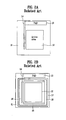
- FIGs. 1A and 1B are plane views illustrating a process of fabricating a passive type organic EL device according to the related art.
- an indium tin oxide (ITO) strip 2 serving as anode is formed on a glass substrate 1 as shown in FIG. 1.
- a short ITO strip 2-1 is formed at a portion where one end of cathode is being formed, simultaneously with the formation of the ITO strip 2. Forming the short ITO strip 2-1 in advance is to make it easy to form a metal extension line to be connected with cathode.
- an auxiliary electrode is formed on the ITO strips 2 and 2-1, and then an insulating layer 3 is formed on the auxiliary electrode. Next, for insulation between cathodes, an electrical insulation separator 4 is formed.
- an organic EL layer 5 including a hole transporting layer, an emission layer and an electron transporting layer is coated and then a cathode 6 is formed of a conductive material such as an Mg-Ag alloy, aluminum (Al).
- the cathode 6 can contact the short ITO strip 2-1 by not forming the organic EL layer 5 on the short ITO strip 2-1 but forming the cathode 6 on the short ITO strip 2-1.
- a seal plate 8 is attached on a resultant structure by a sealant 7, thereby completing the passive type organic EL device.
- FIGs. 2A and 2B are plane views illustrating a process of fabricating an active type organic EL device according to the related art.
- an active area 12 and a pad 13 are formed on a glass substrate 11.
- a metal line 14 electrically connected with the pad is formed at a portion where one end of a cathode is positioned so as to make it easy to connect the metal line 14 with the cathode.
- the active area 12 includes a plurality of unit cells arranged in a matrix configuration, each unit cell including a drive transistor (TFT) and an anode connected to drain electrode of the drive TFT.
- TFT drive transistor
- an organic EL layer 15 is formed on the active area 12.
- the organic EL layer 15 should not be formed on the metal line 14 so that the metal line 14 may contact the cathode to be formed later.
- a cathode 16 is formed on the organic EL layer 15. At this time, the cathode 16 is formed extending to an upper surface of the metal line 14 such that the cathode 16 can contact the metal line 14.
- a passivation layer (not shown) including an oxygen adsorbent layer, a moisture absorbent layer and a moisture permeation preventing layer is formed on a resultant structure and then a seal plate 18 is attached on the passivation layer using a sealant 17, thereby completing the active type organic EL display panel.
- the above organic EL device is required to form first the organic EL layer and secondly the cathode metal film in a vacuum state regardless of whether the organic EL device is the passive type or the active type.
- the metal thin film can be formed by one of three deposition methods consisting of a vacuum evaporation, a sputtering and an ion-plating.
- the vacuum evaporation is the most widely used to form the cathode.
- the vacuum evaporation can be further classified into four types consisting of a resistance heating evaporation, an E-beam heating evaporation, a RF heating evaporation, and a laser beam heating evaporation.
- the resistance heating evaporation is the most widely used to form the cathode.
- FIG. 3 is a schematic view illustrating a resistance heating evaporation process.
- a target material to be evaporated for example, a boat 31 filled with aluminum (Al) is disposed at a lower side of a chamber.
- a substrate 32 is positioned at a sample holder disposed at an upper side of the chamber, and then a mask 33 is aligned below the substrate 32 such that a thin film having a desired pattern corresponding to a pattern of the mask 33 is formed on the substrate 32.
- the chamber is made in a vacuum state and the boat 31 is heated by applying a current thereto, so that the A1 received in the boat 31 is evaporated.
- the evaporated A1 molecules are deposited on the substrate 32 to form a cathode 34.
- the above resistance heating evaporation process has disadvantages such as many preheating time and frequent exchange of the boat due to limitation in capacity of the boat receiving the target material.
- the E-beam heating evaporation process having a faster preheating time than in the resistance heating evaporation process and using a crucible instead of the boat is presently employed in the mass production.
- FIG. 4 is a schematic view illustrating an E-beam heating evaporation process.
- a target material to be evaporated for example, a crucible 41 filled with aluminum (Al) is loaded at a lower side of a chamber.
- a substrate 42 is positioned at a sample holder disposed at an upper side of the chamber, and then a mask 43 is aligned below the substrate 42 such that a thin film having a desired pattern corresponding to a pattern of the mask 43 is formed on the substrate 42.
- a filament 44 emitting electrons is positioned at a side portion of the crucible 41, and a magnet 45 is also positioned around the crucible 41 so as to provide a magnetic force for transferring the electrons emitted from the filament 44 to the crucible 41.
- the filament 44 is heated, electrons are emitted therefrom.
- the emitted electrons are curved in the form of a circle by the magnetic force of the magnet 45 and collide with a center of the A1 target material.
- the A1 target material is heated up to an evaporation temperature due to the electrons having a high energy and is evaporated.
- the evaporated A1 molecules are deposited on the substrate 42 to form the cathode 46.
- the present invention is directed to an organic EL device and a driving apparatus thereof that substantially obviate one or more problems due to limitations and disadvantages of the related art.
- An object of the present invention is to provide an organic EL device and fabrication method thereof that can prevent the performance of the organic EL layer and the TFT from being lowered in forming the cathode using an E-beam heating evaporation process.
- an organic EL device comprising a substrate, an anode, an organic EL layer, a cathode, a transparent electrode connected with the cathode to extract the cathode to an outside, and an interconnection line connected to the transparent electrode, for discharging charges accumulated on the cathode outside the organic EL device.
- a method for fabricating an organic EL device comprising a substrate, an anode, an organic EL layer, a cathode, and a transparent electrode connected with the cathode to extract the cathode to an outside, the method comprising: forming an interconnection line connected to the transparent electrode, for discharging charges accumulated on the cathode outside the organic EL device.
- FIGs. 1A and 1B are plane views illustrating a process of fabricating a passive type organic EL device according to the related art
- FIGs. 2A and 2B are plane views illustrating a process of fabricating an active type organic EL device according to the related art
- FIG. 3 is a schematic view illustrating a resistance heating evaporation process
- FIG. 4 is a schematic view illustrating an E-beam heating evaporation process
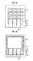
- FIGs. 5A and 5B are plane views illustrating a process of fabricating a passive type organic EL device according to the present invention.
- FIGs. 6A and 6B are plane views illustrating a process of fabricating an active type organic EL device according to the present invention.
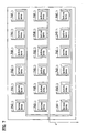
- FIG. 7 is a plane view illustrating an array of at least two organic EL devices on a large-sized substrate according to the present invention.
- FIGs. 5A and 5B are plane views illustrating a process of fabricating a passive type organic EL device according to the present invention.
- an ITO strip 52 serving as anode is formed on a glass substrate 51.
- a short ITO strip 52-1 is formed at a portion where one end of cathode is being formed, simultaneously with the formation of the ITO strip 52. Forming the short ITO strip 2-1 in advance is to make it easy to form a metal extension line to be connected with cathode.
- an interconnection line 52-2 is formed together with the Ito strips 52-1.
- the interconnection line 52-2 is to short the ITO strips 52-1 and thus emit charges accumulated on the cathode while the cathode is formed, outside the glass substrate 51.
- interconnection line 52-2 together with the ITO strip 52-1 corresponds to only a preferred embodiment of the present invention. Since the position of the interconnection line 52-2 is outside the effective display area of the organic EL device, another hole is not formed thereon. Accordingly, the interconnection line 52-2 can be formed whenever in the whole fabrication process.
- the interconnection line 52-2 is formed before the formation of the cathode such that the charges accumulated on the cathode due to the E-beam evaporation are rapidly discharged to an outside.
- the interconnection line 52-2 is made of at least one conductive material selected from the group consisting of Cr, Cu, Mo, W, Au, Ni, Ag, Ti, Ta, Al and AlNd.
- an auxiliary electrode is formed on the ITO strips 52 and 52-1, and then an insulating layer 53 is formed on the auxiliary electrode. Next, for insulation between cathodes, an electrical insulation separator 54 is formed.
- an organic EL layer 55 including a hole transporting layer, an emission layer and an electron transporting layer is coated. At this time, for a contact between the cathode to be formed later and the ITO strip 52-1, the organic EL layer 55 is not formed on the ITO strip 52-1.
- a cathode 56 is formed of a conductive material such as an Mg-Ag alloy, aluminum (Al) by the E-beam evaporation process.
- the cathode 56 can contact the short ITO strip 52-1 by forming the cathode 6 on the short ITO strip 52-1.
- a seal plate 58 is attached on a resultant structure by a sealant 57, thereby completing the passive type organic EL device.
- FIGs. 6A and 6B are plane views illustrating a process of fabricating an active type organic EL device according to the present invention.
- an active area 62 and a pad 63 are formed on a glass substrate 61.
- a first interconnection line 64 electrically connected with the pad 63 is formed at a portion where one end of a cathode is positioned so as to make it easy to connect the first interconnection line 64 with the cathode.
- a second interconnection line 65 is formed at a portion where the other end of the cathode is positioned.
- the second interconnection line 65 is to extract charges accumulated during the formation of the cathode to an outside of the glass substrate 61.
- the active area 62 includes a plurality of unit cells arranged in a matrix configuration, each unit cell including a drive transistor (TFT) and an anode connected to drain electrode of the drive TFT.
- TFT drive transistor
- anode connected to drain electrode of the drive TFT.
- An island-shaped semiconductor layer is formed on the glass substrate 61 and then a gate insulating layer is formed on an entire surface of a resultant glass substrate including the semiconductor layer.
- a gate electrode is formed at a portion overlapping a central portion of the semiconductor layer on the gate insulating layer.
- p-type or n-type impurities are implanted into the semiconductor layer using the gate electrode as a mask.
- an annealing is performed to form source region and drain region, thereby completing the drive TFT.
- a contact contacting the source electrode and the drain electrode of the drive TFT is formed penetrating the insulating layer and the gate insulating layer, and then an insulating layer is again formed on an entire surface of a resultant substrate.
- planarization insulating layer and the insulating layer are selectively removed to form a via-hole for exposing a surface of the contact connected with the drain electrode.
- a material for the formation of anode is deposited on the planarization insulating layer including the via-hole such that the via-hole is filled with the material.
- the material deposited for the formation of anode is selectively removed to form anode such that the anode is separated in a pixel unit. Thereafter, an insulating layer is formed on an entire surface except for the emission area to form the active area 62.
- the second interconnection line 65 is formed concurrently with the formation of the first interconnection line 64, which only corresponds to an embodiment of the present invention.
- the second interconnection line 65 may be formed concurrent with the formation of anode of the active area 62, with the formation of the semiconductor layer used as the source and drain electrodes, or with the formation of the gate electrode.
- the second interconnection line 62 may be formed of a conductive material selected from the group consisting of Cr, Cu, Mo, W, Au, Ni, Ag, Ti, Ta, Al and AlNd.
- an organic EL layer 66 is formed on the active area 62.
- the organic EL layer 66 should not be formed on the first and second interconnection lines 64 and 65 so that the first and second interconnection lines 64 and 65 may contact the cathode to be formed later.
- a cathode 67 is formed on the organic EL layer 66 by an E-beam evaporation process. At this time, the cathode 67 is formed extending to an upper surface of the first and second interconnection lines 64 and 65 such that the cathode 67 can contact the first and second interconnection lines 64 and 65.
- a passivation layer (not shown) including an oxygen adsorbent layer, a moisture absorbent layer and a moisture permeation preventing layer is formed on a resultant structure and then a seal plate 69 is attached on the passivation layer using a sealant 68, thereby completing the active type organic EL display panel.
- FIG. 7 is a plane view illustrating an array of at least two organic EL devices on a large-sized substrate used in a mass production according to the present invention.
- FIG. 7 shows that the interconnection lines 65 for extracting charges from each organic EL device are all connected with the respective organic EL devices and extend to an end point of the glass substrate so as to make easy a contact at an outside.
- the organic EL device and fabrication method thereof according to the present invention it is possible to extract charges accumulated on a cathode while an E-beam evaporation is performed for the formation of the cathode, outside the glass substrate. Accordingly, the underlying organic EL layer and the TFT can be prevented from being damaged due to the charges accumulated on the cathode, so that the reliability of the organic EL device can be enhanced.
Landscapes
- Engineering & Computer Science (AREA)
- Microelectronics & Electronic Packaging (AREA)
- Physics & Mathematics (AREA)
- Optics & Photonics (AREA)
- Electroluminescent Light Sources (AREA)
Applications Claiming Priority (2)
| Application Number | Priority Date | Filing Date | Title |
|---|---|---|---|
| KR2003088603 | 2003-12-08 | ||
| KR1020030088603A KR100786071B1 (ko) | 2003-12-08 | 2003-12-08 | 유기 el 소자 및 그의 제조방법 |
Publications (2)
| Publication Number | Publication Date |
|---|---|
| EP1542293A2 true EP1542293A2 (fr) | 2005-06-15 |
| EP1542293A3 EP1542293A3 (fr) | 2006-07-12 |
Family
ID=34511186
Family Applications (1)
| Application Number | Title | Priority Date | Filing Date |
|---|---|---|---|
| EP04028912A Withdrawn EP1542293A3 (fr) | 2003-12-08 | 2004-12-07 | Dispositif électroluminescent organique et méthode de fabrication |
Country Status (5)
| Country | Link |
|---|---|
| US (2) | US7605393B2 (fr) |
| EP (1) | EP1542293A3 (fr) |
| JP (1) | JP3968726B2 (fr) |
| KR (1) | KR100786071B1 (fr) |
| CN (1) | CN100479178C (fr) |
Families Citing this family (6)
| Publication number | Priority date | Publication date | Assignee | Title |
|---|---|---|---|---|
| KR100696519B1 (ko) * | 2005-05-10 | 2007-03-19 | 삼성에스디아이 주식회사 | 유기 발광 소자용 기판 및 유기 발광 소자 |
| TWI330726B (en) * | 2005-09-05 | 2010-09-21 | Au Optronics Corp | Display apparatus, thin-film-transistor discharge method and electrical driving method therefor |
| KR100822204B1 (ko) * | 2006-06-07 | 2008-04-17 | 삼성에스디아이 주식회사 | 유기 발광 디스플레이 장치 |
| JP4752818B2 (ja) | 2007-07-06 | 2011-08-17 | ソニー株式会社 | 有機el表示装置、電子機器、有機el表示装置用の基板および有機el表示装置の製造方法 |
| TWI514050B (zh) * | 2010-12-06 | 2015-12-21 | Hon Hai Prec Ind Co Ltd | 背光膜片及其製造方法與成型設備 |
| CN109147584B (zh) * | 2018-08-10 | 2024-02-09 | 佛山市国星光电股份有限公司 | 一种led显示单元组及显示面板 |
Citations (1)
| Publication number | Priority date | Publication date | Assignee | Title |
|---|---|---|---|---|
| EP1128439A2 (fr) * | 2000-02-28 | 2001-08-29 | Sel Semiconductor Energy Laboratory Co., Ltd. | Dispositif d'affichage électroluminescent à matrice active |
Family Cites Families (19)
| Publication number | Priority date | Publication date | Assignee | Title |
|---|---|---|---|---|
| GB1126966A (en) * | 1965-12-10 | 1968-09-11 | Gen Electric Co Ltd | Improvements in or relating to superconducting magnets |
| KR100409057B1 (ko) * | 1997-12-10 | 2003-12-11 | 가부시끼가이샤 히다치 세이사꾸쇼 | 산화물초전도선, 솔레노이드코일, 자장발생장치 및산화물초전도선의 제조방법 |
| GB9813326D0 (en) * | 1998-06-19 | 1998-08-19 | Cambridge Display Tech Ltd | Backlit displays |
| JP4279391B2 (ja) | 1999-02-16 | 2009-06-17 | 東北パイオニア株式会社 | 発光ディスプレイパネル及びその製造方法 |
| JP3568189B2 (ja) * | 1999-04-21 | 2004-09-22 | 東北パイオニア株式会社 | 有機elディスプレイの製造方法および装置 |
| JP2001109395A (ja) | 1999-10-01 | 2001-04-20 | Sanyo Electric Co Ltd | El表示装置 |
| US6687975B2 (en) * | 2001-03-09 | 2004-02-10 | Hyper Tech Research Inc. | Method for manufacturing MgB2 intermetallic superconductor wires |
| JP4058920B2 (ja) * | 2001-07-10 | 2008-03-12 | 株式会社日立製作所 | 超電導接続構造 |
| DE10133684A1 (de) * | 2001-07-11 | 2003-02-13 | Osram Opto Semiconductors Gmbh | Organisches, farbiges, elektrolumineszierendes Display und dessen Herstellung |
| US6569697B2 (en) * | 2001-08-20 | 2003-05-27 | Universal Display Corporation | Method of fabricating electrodes |
| KR100413455B1 (ko) * | 2001-09-10 | 2003-12-31 | 엘지전자 주식회사 | 정전기 제거용 유기 el 소자 |
| JP2003142258A (ja) | 2001-10-31 | 2003-05-16 | Nippon Seiki Co Ltd | 有機elパネル |
| KR100462046B1 (ko) * | 2001-11-05 | 2004-12-16 | 네오뷰코오롱 주식회사 | 유기물 디스플레이의 무기물막 증착 장치 |
| TWI286044B (en) * | 2002-02-22 | 2007-08-21 | Semiconductor Energy Lab | Light-emitting device and method of manufacturing the same, and method of operating manufacturing apparatus |
| CN100517422C (zh) * | 2002-03-07 | 2009-07-22 | 三洋电机株式会社 | 配线结构、其制造方法、以及光学设备 |
| ITMI20021004A1 (it) * | 2002-05-10 | 2003-11-10 | Edison Spa | Metodo per la realizzazione di fili superconduttori a base di filamenti cavi di mgb2 |
| TW581991B (en) * | 2002-10-25 | 2004-04-01 | Ritdisplay Corp | OLED device and packaging method thereof |
| US7250930B2 (en) * | 2003-02-07 | 2007-07-31 | Hewlett-Packard Development Company, L.P. | Transparent active-matrix display |
| US6995035B2 (en) * | 2003-06-16 | 2006-02-07 | Eastman Kodak Company | Method of making a top-emitting OLED device having improved power distribution |
-
2003
- 2003-12-08 KR KR1020030088603A patent/KR100786071B1/ko not_active Expired - Fee Related
-
2004
- 2004-12-07 EP EP04028912A patent/EP1542293A3/fr not_active Withdrawn
- 2004-12-07 US US11/005,018 patent/US7605393B2/en not_active Expired - Fee Related
- 2004-12-08 CN CNB2004100965947A patent/CN100479178C/zh not_active Expired - Fee Related
- 2004-12-08 JP JP2004355931A patent/JP3968726B2/ja not_active Expired - Fee Related
-
2009
- 2009-02-03 US US12/364,702 patent/US7858435B2/en not_active Expired - Lifetime
Patent Citations (1)
| Publication number | Priority date | Publication date | Assignee | Title |
|---|---|---|---|---|
| EP1128439A2 (fr) * | 2000-02-28 | 2001-08-29 | Sel Semiconductor Energy Laboratory Co., Ltd. | Dispositif d'affichage électroluminescent à matrice active |
Also Published As
| Publication number | Publication date |
|---|---|
| US20050121670A1 (en) | 2005-06-09 |
| JP2005174931A (ja) | 2005-06-30 |
| US7858435B2 (en) | 2010-12-28 |
| CN100479178C (zh) | 2009-04-15 |
| JP3968726B2 (ja) | 2007-08-29 |
| CN1627870A (zh) | 2005-06-15 |
| US7605393B2 (en) | 2009-10-20 |
| US20090142868A1 (en) | 2009-06-04 |
| EP1542293A3 (fr) | 2006-07-12 |
| KR20050055395A (ko) | 2005-06-13 |
| KR100786071B1 (ko) | 2007-12-18 |
Similar Documents
| Publication | Publication Date | Title |
|---|---|---|
| US10229965B2 (en) | Method fabricating organic light emitting diode display device | |
| US7629018B2 (en) | Light emitting device and method of manufacturing the same | |
| US7518147B2 (en) | Organic electro luminescence device and fabrication method thereof | |
| US7686666B2 (en) | Flat panel display device capable of reducing or preventing a voltage drop and method of fabricating the same | |
| JP4049330B2 (ja) | 電界発光ディスプレイ装置及びその製造方法 | |
| US6917160B2 (en) | Organic electroluminescent display and method of manufacturing the same | |
| US20070054051A1 (en) | Deposition device | |
| US7576812B2 (en) | Liquid crystal display device and method for fabricating the same | |
| CN109524576B (zh) | 一种oled显示基板及其制备方法、显示装置 | |
| KR101553942B1 (ko) | 플렉서블 디스플레이 제조장치 | |
| JP4651916B2 (ja) | 発光装置の作製方法 | |
| CN101221972B (zh) | 有机电致发光显示器件及制造有机电致发光二极管的方法 | |
| WO2018045658A1 (fr) | Dispositif d'affichage amoled | |
| US7858435B2 (en) | Organic electro-luminance device and method for fabricating the same | |
| JP4545385B2 (ja) | 発光装置の作製方法 | |
| JP2003272867A (ja) | 発光素子およびアクティブマトリクス型表示装置 | |
| US20050184650A1 (en) | [organic electro-luminescent device and fabricating method thereof] | |
| KR20160141270A (ko) | 유기발광다이오드 및 그 제조 방법 | |
| JP2005005159A (ja) | 有機el装置とその製造方法、並びに電子機器 | |
| KR102959899B1 (ko) | Oled 디스플레이 소자 | |
| KR100669316B1 (ko) | 유기 전계 발광 표시 장치 | |
| KR100414296B1 (ko) | 유기 전계 발광 소자의 패키징 구조 및 그 제조 방법 | |
| KR100741781B1 (ko) | 양면 표시 장치 | |
| JP2001196168A (ja) | 有機エレクトロルミネッセンス素子の製造方法 | |
| JP2005228558A (ja) | 表示体製造方法、表示体及び電子機器 |
Legal Events
| Date | Code | Title | Description |
|---|---|---|---|
| PUAI | Public reference made under article 153(3) epc to a published international application that has entered the european phase |
Free format text: ORIGINAL CODE: 0009012 |
|
| 17P | Request for examination filed |
Effective date: 20041208 |
|
| AK | Designated contracting states |
Kind code of ref document: A2 Designated state(s): AT BE BG CH CY CZ DE DK EE ES FI FR GB GR HU IE IS IT LI LT LU MC NL PL PT RO SE SI SK TR |
|
| AX | Request for extension of the european patent |
Extension state: AL BA HR LV MK YU |
|
| PUAL | Search report despatched |
Free format text: ORIGINAL CODE: 0009013 |
|
| AK | Designated contracting states |
Kind code of ref document: A3 Designated state(s): AT BE BG CH CY CZ DE DK EE ES FI FR GB GR HU IE IS IT LI LT LU MC NL PL PT RO SE SI SK TR |
|
| AX | Request for extension of the european patent |
Extension state: AL BA HR LV MK YU |
|
| AKX | Designation fees paid |
Designated state(s): DE FR GB NL |
|
| 17Q | First examination report despatched |
Effective date: 20071106 |
|
| GRAP | Despatch of communication of intention to grant a patent |
Free format text: ORIGINAL CODE: EPIDOSNIGR1 |
|
| RIC1 | Information provided on ipc code assigned before grant |
Ipc: H01L 27/32 20060101AFI20121009BHEP Ipc: H01L 51/52 20060101ALI20121009BHEP |
|
| STAA | Information on the status of an ep patent application or granted ep patent |
Free format text: STATUS: THE APPLICATION IS DEEMED TO BE WITHDRAWN |
|
| 18D | Application deemed to be withdrawn |
Effective date: 20130301 |