EP1544917A1 - Bloc de batterie intégré, relié à une grille de connexion - Google Patents
Bloc de batterie intégré, relié à une grille de connexion Download PDFInfo
- Publication number
- EP1544917A1 EP1544917A1 EP03392012A EP03392012A EP1544917A1 EP 1544917 A1 EP1544917 A1 EP 1544917A1 EP 03392012 A EP03392012 A EP 03392012A EP 03392012 A EP03392012 A EP 03392012A EP 1544917 A1 EP1544917 A1 EP 1544917A1
- Authority
- EP
- European Patent Office
- Prior art keywords
- lead frame
- battery
- package
- assembly
- semiconductor chips
- Prior art date
- Legal status (The legal status is an assumption and is not a legal conclusion. Google has not performed a legal analysis and makes no representation as to the accuracy of the status listed.)
- Withdrawn
Links
Images



Classifications
-
- H—ELECTRICITY
- H10—SEMICONDUCTOR DEVICES; ELECTRIC SOLID-STATE DEVICES NOT OTHERWISE PROVIDED FOR
- H10W—GENERIC PACKAGES, INTERCONNECTIONS, CONNECTORS OR OTHER CONSTRUCTIONAL DETAILS OF DEVICES COVERED BY CLASS H10
- H10W42/00—Arrangements for protection of devices
-
- H—ELECTRICITY
- H10—SEMICONDUCTOR DEVICES; ELECTRIC SOLID-STATE DEVICES NOT OTHERWISE PROVIDED FOR
- H10W—GENERIC PACKAGES, INTERCONNECTIONS, CONNECTORS OR OTHER CONSTRUCTIONAL DETAILS OF DEVICES COVERED BY CLASS H10
- H10W72/00—Interconnections or connectors in packages
- H10W72/50—Bond wires
- H10W72/531—Shapes of wire connectors
- H10W72/536—Shapes of wire connectors the connected ends being ball-shaped
-
- H—ELECTRICITY
- H10—SEMICONDUCTOR DEVICES; ELECTRIC SOLID-STATE DEVICES NOT OTHERWISE PROVIDED FOR
- H10W—GENERIC PACKAGES, INTERCONNECTIONS, CONNECTORS OR OTHER CONSTRUCTIONAL DETAILS OF DEVICES COVERED BY CLASS H10
- H10W72/00—Interconnections or connectors in packages
- H10W72/50—Bond wires
- H10W72/531—Shapes of wire connectors
- H10W72/5363—Shapes of wire connectors the connected ends being wedge-shaped
-
- H—ELECTRICITY
- H10—SEMICONDUCTOR DEVICES; ELECTRIC SOLID-STATE DEVICES NOT OTHERWISE PROVIDED FOR
- H10W—GENERIC PACKAGES, INTERCONNECTIONS, CONNECTORS OR OTHER CONSTRUCTIONAL DETAILS OF DEVICES COVERED BY CLASS H10
- H10W90/00—Package configurations
- H10W90/701—Package configurations characterised by the relative positions of pads or connectors relative to package parts
- H10W90/751—Package configurations characterised by the relative positions of pads or connectors relative to package parts of bond wires
- H10W90/756—Package configurations characterised by the relative positions of pads or connectors relative to package parts of bond wires between a chip and a stacked lead frame, conducting package substrate or heat sink
-
- Y—GENERAL TAGGING OF NEW TECHNOLOGICAL DEVELOPMENTS; GENERAL TAGGING OF CROSS-SECTIONAL TECHNOLOGIES SPANNING OVER SEVERAL SECTIONS OF THE IPC; TECHNICAL SUBJECTS COVERED BY FORMER USPC CROSS-REFERENCE ART COLLECTIONS [XRACs] AND DIGESTS
- Y02—TECHNOLOGIES OR APPLICATIONS FOR MITIGATION OR ADAPTATION AGAINST CLIMATE CHANGE
- Y02P—CLIMATE CHANGE MITIGATION TECHNOLOGIES IN THE PRODUCTION OR PROCESSING OF GOODS
- Y02P70/00—Climate change mitigation technologies in the production process for final industrial or consumer products
- Y02P70/50—Manufacturing or production processes characterised by the final manufactured product
-
- Y—GENERAL TAGGING OF NEW TECHNOLOGICAL DEVELOPMENTS; GENERAL TAGGING OF CROSS-SECTIONAL TECHNOLOGIES SPANNING OVER SEVERAL SECTIONS OF THE IPC; TECHNICAL SUBJECTS COVERED BY FORMER USPC CROSS-REFERENCE ART COLLECTIONS [XRACs] AND DIGESTS
- Y10—TECHNICAL SUBJECTS COVERED BY FORMER USPC
- Y10T—TECHNICAL SUBJECTS COVERED BY FORMER US CLASSIFICATION
- Y10T29/00—Metal working
- Y10T29/49—Method of mechanical manufacture
- Y10T29/49002—Electrical device making
- Y10T29/49108—Electric battery cell making
Definitions
- This invention relates generally to a battery assembly, and more particularly to an assembly technique to incorporate electronic functions within removable battery packs, where all components are interconnected using a lead frame technology.
- chip-carrier typically a lead frame in today's technology
- a printed circuit board Further connecting devices would then connect to said printed circuit board.
- a plastic case with a bottom and top element would then enclose the whole assembly
- Integrated semiconductor modules often use the lead frame technology to carry the semiconductor chip and to connect the chip pads with a larger printed circuit board.
- These lead frames are normally encapsulated with a convenient plastic material.
- Fig 1 shows the cross sections of two typical examples of said semiconductor modules.
- Fig. 2 shows a bare lead frame, which is produced as a long tape of metal sheet.
- the basic material of lead frames is sheet metal.
- the leads are either metal-stamped or etched to form the leads, therefore complex forms of said leads can be achieved.
- the leads are typically pre-formed in a bending process to accommodate all kinds of shapes. A frame area around all leads holds said leads in position, until the chips are mounted and the assembly has been encapsulated (molded) into plastic material.
- U. S. Patent (5,498,903 to Dioxin et al.) describes an integrated circuit package of the surface-mountable type within which a battery is mounted.
- Battery leads extend from the side of the package body opposite that which is adjacent the circuit board when mounted, and between which a conventional battery may be placed.
- a gap is present between the housing and the battery. The gaps thermally insulate the battery from the package body and housing, so that the circuit may be subjected to solder reflow mounting to a circuit board, while insulating the high temperature from the battery.
- U. S. Patent (6,109,530 to Larson et al.) discloses a chip-battery micro-module and fabrication there of wherein an integrated circuit "chip" is secured to a battery coin cell using various conductive and insulating layers that provide power to the chip.
- the chip-battery micro-module may be used to power an electronic accessory that is directly attached thereto, such as an LCD display or speaker, or to power a circuit in a smart card or electronic device such as a portable phone.
- the chip battery micro-module can be integrated into a plastic smart card.
- U. S. Patent (6,284,406 B1 to Xing et al) shows an IC card comprising an electronic device and a battery within a plastic card for electrically energizing the electronic device.
- the battery is comprised as a monolithic electro-chemical cell having a lithium-containing cathode, a carbon anode, and a porous polymer separator infused with electrolyte solution.
- the cell has a thickness of less than 0.7 mm.
- the battery has an overall thickness of less than 0.8 mm.
- a principal object of the invention described herein is to build an integrated battery package, that contains semiconductor chips, for example to control and regulate battery charging and to monitor package operation, and that interconnects several of said internal chips, connects said chips to the battery within the package and connects the whole package assembly to the outside.
- the basic aspects of an assembly are to reduce the connection devices to a minimum and where the package is a smooth sided box.
- a single lead frame serves several purposes: it connects the, possibly multi-chip electronic circuits, it connects the battery cells to said multichip circuit and it forms, without any additional parts, the external connectors of the completed package.
- a molding process similar to some semiconductor module packaging technologies, encapsulates the inner section of the lead frame together with the assembled semiconductor chips and possibly other electrical components with plastic material into a small, probably flat, package.
- said mold is designed to form the bottom structure of the total package within that same production step.
- leads of the lead frame are pre-formed to attach to the battery cells.
- Two or more leads of said single lead frame are also pre-formed to finally build the external contacts.
- the package will be closed and sealed with a top cover, leaving only the essential external contacts being exposed outside.
- the lead frame may internally connect one or more semiconductor chips; it may also interconnect to other active and/or passive components, like capacitors.
- Some of said leads of said lead frame will be formed to accommodate a connection to said battery cells and other leads will be formed to build the external connection of the final package assembly.
- Forming of said leads can be realized during the original manufacturing process of said lead frames or pre-forming can be processed as a separate bending process before the electronic components are mounted to said lead frame. A separate bending process can even be performed after said semiconductor and other chips are mounted to said lead frame and after the inner section of the lead frame together with said mounted chips is encapsulated.
- said molding process encapsulating said semiconductor chips and the inner area of the lead frame, also forms the body structure of said battery package with an optimized design of said mold.
- the body preferably designed as a flat structure, can also accommodate the fixture for said battery cells and form a lid to hold a top cover in place.
- the lead frame can be manufactured in one of several processes, for example metal stamping and metal etching.
- Semiconductor chips and said passive components may be attached to said lead frame with a known technique, like wire bonding, solder balls, solder pads and similar established processes.
- the outer frame After molding the inner section, the outer frame, which holds the leads in their position during the manufacturing process, is cut away.
- the battery cells could be electrically contacted to said leads by welding or with conductive adhesives or by similar means.
- the external connector may be placed on the same side or on opposites sides of the package and they may be placed in the bottom surface, parallel to the lead frame plane.
- the whole battery package will most likely be closed with an additional cover element, put over the mounted battery cells and sealed to said body of the package.
- the pre-formed external contacts are then the only remaining connection to the package outside.
- a principal object of the invention described in the present document is to build an integrated battery package in a smooth sided box, that contains semiconductor chips, for example to control and regulate battery charging and to monitor package operation, and that interconnects several of said internal chips, connects said chips to the battery within the package and connects the whole package to the outside.
- the basic aspect is to reduce the connection devices to a minimum.
- the disclosed invention uses a similar lead frame technology and a similar molding technology, as used for semiconductor module packaging.
- a single lead frame specially designed for the envisioned purpose, is used.
- said lead frame serves several purposes at the same time: the first is to connect to the, possibly multi-chip electronic circuits, second, it connects the battery cells to said multichip circuit and it forms and third, without any additional parts, it builds the external connectors of the completed package.
- Lead frames can be manufactured in one of several processes, for example metal stamping and metal etching.
- the outer Frame out-Frame 3 holds all leads during the manufacturing process in place. Some of said leads of said lead frame will be formed to accommodate a connection to said battery cells and other leads will be formed to build the external connection of the final package.
- ChipCon 3 are the connection areas where the various chips will later be contacted. pref-Lead 3 points to the preformed leads for battery cells and for external package contacts.
- Fig. 4 shows said lead frame with the semiconductor chips Chip and the passive components pass-Comp mounted.
- the semiconductor chips and said passive components may be attached to said lead frame with a known technique, like wire bonding, solder balls, solder pads and similar established processes.
- Typical semiconductor modules encapsulate the inner section of the lead frame together with the connected chip by molding this assembly with convenient plastic material into a small, often flat, package.
- a similar molding concept and process is used for this invention, however additionally the mold is designed to form the bottom body of the total package in that same production step.
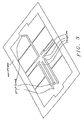
- the result of said molding process is shown in Fig. 5 , the lead frame and the already mounted chips are encapsulated with a plastic material.
- the resulting structure will also serve as the body Body 5 of the total package.
- the chips are now buried inside the molded part, only said connections for battery cells Batt-Conn 5 and external connections ext-Conn 5 remain visible.
- Forming said leads could be realized during the original manufacturing process of said lead frames.
- Pre-forming can also be processed as a separate bending process before said semiconductor and other chips are mounted to said lead frame.
- a separate bending process can even be performed after said semiconductor and other chips are mounted to said lead frame and after the inner section of the lead frame together with said mounted chips is encapsulated by molding the lead frame and chip assembly.
- Fig. 7 a principal concept for a possible solution is presented in Fig. 7 , with the body Body 7 and the battery Batt .
- the battery cells could be electrically contacted to said battery connection Batt-Conn 7 , by welding or with conductive adhesives or by similar means.
- Fig. 8 the cover Cover is put over the assembled body and battery Body 8 and the package may be sealed.
- the pre-formed external contacts ext-Conn 8 are then the only remaining connection to the package outside.
- the external connector may be placed, for example, on the same side or on opposites sides of the package and they may be placed in the bottom surface, parallel to the lead frame plane.
- Fig 9 and Fig. 10 show two possible examples for positioning said external contacts.
- Sem-Chip 9 and Sem-Chip 10 are the semiconductor chips, contacted to said lead frame with solder balls Batt Conn 1 9/1 10 and Batt Conn 2 9/2 10 are the battery connection in this example; Ext Conn right is a possible solution as shown in Fig. 9; Ext Conn bottom is a similar solution as shown in Fig. 10
- a flat lead frame is produced by stamping or etching or a similar process.
- the leads for battery connection and for external connectors may be pre-formed.
- the semiconductor chips, and possibly other passive components are mounted 114 .
- the semiconductor chips and other passive components will be electrically connected to the lead frame.
- the inner section of lead frame and the mounted chips and components are encapsulated with plastic material by the molding process, step 116 .
- the same molding process also forms the package body, 117 .
- the battery cells will be mounted and the battery contacts are welded or glued to the battery cells 119 . Now close and seal the package with a top cover in the final step 120 .
Landscapes
- Battery Mounting, Suspending (AREA)
Priority Applications (3)
| Application Number | Priority Date | Filing Date | Title |
|---|---|---|---|
| EP03392012A EP1544917A1 (fr) | 2003-12-15 | 2003-12-15 | Bloc de batterie intégré, relié à une grille de connexion |
| US10/756,700 US7332363B2 (en) | 2003-12-15 | 2004-01-13 | Integrated battery pack with lead frame connection |
| US12/008,153 US7791179B2 (en) | 2003-12-15 | 2008-01-09 | Integrated battery pack with lead frame connection |
Applications Claiming Priority (1)
| Application Number | Priority Date | Filing Date | Title |
|---|---|---|---|
| EP03392012A EP1544917A1 (fr) | 2003-12-15 | 2003-12-15 | Bloc de batterie intégré, relié à une grille de connexion |
Publications (1)
| Publication Number | Publication Date |
|---|---|
| EP1544917A1 true EP1544917A1 (fr) | 2005-06-22 |
Family
ID=34486532
Family Applications (1)
| Application Number | Title | Priority Date | Filing Date |
|---|---|---|---|
| EP03392012A Withdrawn EP1544917A1 (fr) | 2003-12-15 | 2003-12-15 | Bloc de batterie intégré, relié à une grille de connexion |
Country Status (2)
| Country | Link |
|---|---|
| US (2) | US7332363B2 (fr) |
| EP (1) | EP1544917A1 (fr) |
Cited By (2)
| Publication number | Priority date | Publication date | Assignee | Title |
|---|---|---|---|---|
| FR2912261A1 (fr) * | 2007-02-07 | 2008-08-08 | Peugeot Citroen Automobiles Sa | Dispositif de fourniture d'energie electrique |
| US12266817B2 (en) | 2021-02-03 | 2025-04-01 | Cummins Inc. | Battery pack housing |
Families Citing this family (32)
| Publication number | Priority date | Publication date | Assignee | Title |
|---|---|---|---|---|
| US8404376B2 (en) | 2002-08-09 | 2013-03-26 | Infinite Power Solutions, Inc. | Metal film encapsulation |
| US7993773B2 (en) | 2002-08-09 | 2011-08-09 | Infinite Power Solutions, Inc. | Electrochemical apparatus with barrier layer protected substrate |
| US8445130B2 (en) | 2002-08-09 | 2013-05-21 | Infinite Power Solutions, Inc. | Hybrid thin-film battery |
| US8394522B2 (en) | 2002-08-09 | 2013-03-12 | Infinite Power Solutions, Inc. | Robust metal film encapsulation |
| US8431264B2 (en) | 2002-08-09 | 2013-04-30 | Infinite Power Solutions, Inc. | Hybrid thin-film battery |
| US8236443B2 (en) | 2002-08-09 | 2012-08-07 | Infinite Power Solutions, Inc. | Metal film encapsulation |
| US20070264564A1 (en) | 2006-03-16 | 2007-11-15 | Infinite Power Solutions, Inc. | Thin film battery on an integrated circuit or circuit board and method thereof |
| US8021778B2 (en) * | 2002-08-09 | 2011-09-20 | Infinite Power Solutions, Inc. | Electrochemical apparatus with barrier layer protected substrate |
| US8728285B2 (en) | 2003-05-23 | 2014-05-20 | Demaray, Llc | Transparent conductive oxides |
| US7557433B2 (en) | 2004-10-25 | 2009-07-07 | Mccain Joseph H | Microelectronic device with integrated energy source |
| US8636876B2 (en) | 2004-12-08 | 2014-01-28 | R. Ernest Demaray | Deposition of LiCoO2 |
| US7959769B2 (en) | 2004-12-08 | 2011-06-14 | Infinite Power Solutions, Inc. | Deposition of LiCoO2 |
| CN101523571A (zh) | 2006-09-29 | 2009-09-02 | 无穷动力解决方案股份有限公司 | 柔性基板上沉积的电池层的掩模和材料限制 |
| US8197781B2 (en) | 2006-11-07 | 2012-06-12 | Infinite Power Solutions, Inc. | Sputtering target of Li3PO4 and method for producing same |
| DE102006058068B4 (de) * | 2006-12-07 | 2018-04-05 | Infineon Technologies Ag | Halbleiterbauelement mit Halbleiterchip und passivem Spulen-Bauelement sowie Verfahren zu dessen Herstellung |
| US20090061302A1 (en) * | 2007-09-04 | 2009-03-05 | Scott John S | Battery pack including an electric harness and method of manufacturing the same |
| DE102007050608A1 (de) * | 2007-10-23 | 2009-04-30 | Infineon Technologies Ag | Gehäuse für einen Halbleiter-Chip |
| KR20150128817A (ko) | 2007-12-21 | 2015-11-18 | 사푸라스트 리써치 엘엘씨 | 전해질 막을 위한 표적을 스퍼터링하는 방법 |
| US8268488B2 (en) | 2007-12-21 | 2012-09-18 | Infinite Power Solutions, Inc. | Thin film electrolyte for thin film batteries |
| WO2009089417A1 (fr) | 2008-01-11 | 2009-07-16 | Infinite Power Solutions, Inc. | Encapsulation de films minces pour batteries à film mince et autres dispositifs |
| KR101672254B1 (ko) | 2008-04-02 | 2016-11-08 | 사푸라스트 리써치 엘엘씨 | 에너지 수확과 관련된 에너지 저장 장치를 위한 수동적인 과전압/부족전압 제어 및 보호 |
| EP2319101B1 (fr) | 2008-08-11 | 2015-11-04 | Sapurast Research LLC | Dispositif à énergie doté d une surface de collecteur solidaire pour la collecte d une énergie électromagnétique et son procédé |
| EP2332127A4 (fr) | 2008-09-12 | 2011-11-09 | Infinite Power Solutions Inc | Dispositif d'énergie ayant une surface conductrice intégrée pour une communication de données par l'intermédiaire d'une énergie électromagnétique et procédé associé |
| JP5405785B2 (ja) | 2008-09-19 | 2014-02-05 | ルネサスエレクトロニクス株式会社 | 半導体装置 |
| WO2010042594A1 (fr) | 2008-10-08 | 2010-04-15 | Infinite Power Solutions, Inc. | Module de capteurs sans fil alimenté par l’environnement |
| KR101792287B1 (ko) | 2009-09-01 | 2017-10-31 | 사푸라스트 리써치 엘엘씨 | 집적된 박막 배터리를 갖는 인쇄 회로 보드 |
| KR101930561B1 (ko) | 2010-06-07 | 2018-12-18 | 사푸라스트 리써치 엘엘씨 | 재충전 가능한 고밀도 전기 화학 장치 |
| US20190097524A1 (en) * | 2011-09-13 | 2019-03-28 | Fsp Technology Inc. | Circuit having snubber circuit in power supply device |
| US9343715B2 (en) * | 2013-10-07 | 2016-05-17 | ZeroLemon LLC | Extended battery |
| US9705121B2 (en) * | 2014-08-18 | 2017-07-11 | Johnson Controls Technology Company | Lead frame for a battery module |
| US11223087B2 (en) | 2017-04-24 | 2022-01-11 | A123 Systems Llc | Structural potting material used to increase crush resistance |
| US12469773B2 (en) * | 2022-11-29 | 2025-11-11 | Nxp Usa, Inc. | Semiconductor device with attached battery and method therefor |
Citations (7)
| Publication number | Priority date | Publication date | Assignee | Title |
|---|---|---|---|---|
| US4645943A (en) * | 1984-10-15 | 1987-02-24 | Dallas Semiconductor Corporation | Space-saving back-up power supply |
| US5119269A (en) * | 1989-08-23 | 1992-06-02 | Seiko Epson Corporation | Semiconductor with a battery unit |
| US5451715A (en) * | 1993-08-11 | 1995-09-19 | Sgs-Thomson Microelectronics, Inc. | Molded package integrated circuit with electrochemical cell |
| US5498903A (en) * | 1992-12-21 | 1996-03-12 | Sgs-Thomson Microelectronics, Inc. | Surface mountable integrated circuit package with integrated battery mount |
| US6191955B1 (en) * | 1994-10-28 | 2001-02-20 | Dallas Semiconductor Corporation | Encapsulation and enclosure of electronic modules |
| WO2001097583A2 (fr) * | 2000-06-12 | 2001-12-20 | Bourns, Inc. | Ensemble electronique moule |
| US20020004163A1 (en) * | 2000-07-10 | 2002-01-10 | Fuji Photo Film Co.,Ltd. | IC device, circuit board and IC assembly |
Family Cites Families (11)
| Publication number | Priority date | Publication date | Assignee | Title |
|---|---|---|---|---|
| US4391531A (en) * | 1980-12-19 | 1983-07-05 | Timex Corporation | Electrooptical display/lead frame subassembly and timepiece module including same |
| US5055704A (en) * | 1984-07-23 | 1991-10-08 | Sgs-Thomson Microelectronics, Inc. | Integrated circuit package with battery housing |
| US5294829A (en) * | 1990-01-26 | 1994-03-15 | Sgs-Thomson Microelectronics, Inc. | IC package having direct attach backup battery |
| US5629604A (en) | 1992-11-13 | 1997-05-13 | Zenith Data Systems Corporation | Computer power supply system |
| US5570273A (en) * | 1993-08-31 | 1996-10-29 | Sgs-Thomson Microelectronics, Inc. | Surface mountable integrated circuit package with low-profile detachable module |
| JP3998732B2 (ja) * | 1994-08-31 | 2007-10-31 | エスティーマイクロエレクトロニクス,インコーポレイテッド | 回路部品パッケージ及びその製造方法 |
| US5541530A (en) * | 1995-05-17 | 1996-07-30 | Altera Corporation | Programmable logic array integrated circuits with blocks of logic regions grouped into super-blocks |
| US5914534A (en) | 1996-05-03 | 1999-06-22 | Ford Motor Company | Three-dimensional multi-layer molded electronic device and method for manufacturing same |
| US6072299A (en) * | 1998-01-26 | 2000-06-06 | Medtronic Physio-Control Manufacturing Corp. | Smart battery with maintenance and testing functions |
| US6109530A (en) | 1998-07-08 | 2000-08-29 | Motorola, Inc. | Integrated circuit carrier package with battery coin cell |
| US6284406B1 (en) * | 2000-06-09 | 2001-09-04 | Ntk Powerdex, Inc. | IC card with thin battery |
-
2003
- 2003-12-15 EP EP03392012A patent/EP1544917A1/fr not_active Withdrawn
-
2004
- 2004-01-13 US US10/756,700 patent/US7332363B2/en not_active Expired - Fee Related
-
2008
- 2008-01-09 US US12/008,153 patent/US7791179B2/en not_active Expired - Fee Related
Patent Citations (7)
| Publication number | Priority date | Publication date | Assignee | Title |
|---|---|---|---|---|
| US4645943A (en) * | 1984-10-15 | 1987-02-24 | Dallas Semiconductor Corporation | Space-saving back-up power supply |
| US5119269A (en) * | 1989-08-23 | 1992-06-02 | Seiko Epson Corporation | Semiconductor with a battery unit |
| US5498903A (en) * | 1992-12-21 | 1996-03-12 | Sgs-Thomson Microelectronics, Inc. | Surface mountable integrated circuit package with integrated battery mount |
| US5451715A (en) * | 1993-08-11 | 1995-09-19 | Sgs-Thomson Microelectronics, Inc. | Molded package integrated circuit with electrochemical cell |
| US6191955B1 (en) * | 1994-10-28 | 2001-02-20 | Dallas Semiconductor Corporation | Encapsulation and enclosure of electronic modules |
| WO2001097583A2 (fr) * | 2000-06-12 | 2001-12-20 | Bourns, Inc. | Ensemble electronique moule |
| US20020004163A1 (en) * | 2000-07-10 | 2002-01-10 | Fuji Photo Film Co.,Ltd. | IC device, circuit board and IC assembly |
Cited By (2)
| Publication number | Priority date | Publication date | Assignee | Title |
|---|---|---|---|---|
| FR2912261A1 (fr) * | 2007-02-07 | 2008-08-08 | Peugeot Citroen Automobiles Sa | Dispositif de fourniture d'energie electrique |
| US12266817B2 (en) | 2021-02-03 | 2025-04-01 | Cummins Inc. | Battery pack housing |
Also Published As
| Publication number | Publication date |
|---|---|
| US20080116550A1 (en) | 2008-05-22 |
| US7332363B2 (en) | 2008-02-19 |
| US7791179B2 (en) | 2010-09-07 |
| US20050129989A1 (en) | 2005-06-16 |
Similar Documents
| Publication | Publication Date | Title |
|---|---|---|
| US7791179B2 (en) | Integrated battery pack with lead frame connection | |
| EP0605987B1 (fr) | Boîtier de IC montable à surface avec le montage de batterie intégré | |
| US7230321B2 (en) | Integrated circuit package with laminated power cell having coplanar electrode | |
| US9012264B2 (en) | Integrated circuit package including embedded thin-film battery | |
| US6492726B1 (en) | Chip scale packaging with multi-layer flip chip arrangement and ball grid array interconnection | |
| EP1989739B1 (fr) | Boitier de circuit integre a puces multiples et procédé de fabrication | |
| US5939779A (en) | Bottom lead semiconductor chip stack package | |
| US7855441B2 (en) | Semiconductor card package and method of forming the same | |
| EP1855316A1 (fr) | Boitier de circuit integre empilable | |
| WO2003102601A1 (fr) | Boitier capteur | |
| US20070158810A1 (en) | Stacked integrated circuit package-in-package system | |
| EP1914860A2 (fr) | Module de circuit | |
| US5451715A (en) | Molded package integrated circuit with electrochemical cell | |
| CN113659185B (zh) | 电池保护电路封装件的制造方法 | |
| JPH11214596A (ja) | 半導体装置及びその製造方法並びに電子機器 | |
| US6654218B1 (en) | Protection circuit module for rechargeable battery and method of making the same | |
| US6404100B1 (en) | Surface acoustic wave apparatus and method of manufacturing the same | |
| KR100422608B1 (ko) | 적층칩패키지 | |
| US7019387B1 (en) | Lead-frame connector and circuit module assembly | |
| EP4576177A1 (fr) | Boîtiers de dispositif à batteries intégrées | |
| CN113809031A (zh) | 具有带集成电引线的帽的半导体器件封装 | |
| US20200203259A1 (en) | Integrated circuit package | |
| JP2001203301A (ja) | 樹脂封止型半導体装置及びその製造方法 | |
| KR20210105213A (ko) | 노트북 배터리 보호회로 패키지 및 그 제조 방법 | |
| EP4579742A1 (fr) | Boîtier électronique à couvercle contenant une batterie |
Legal Events
| Date | Code | Title | Description |
|---|---|---|---|
| PUAI | Public reference made under article 153(3) epc to a published international application that has entered the european phase |
Free format text: ORIGINAL CODE: 0009012 |
|
| AK | Designated contracting states |
Kind code of ref document: A1 Designated state(s): AT BE BG CH CY CZ DE DK EE ES FI FR GB GR HU IE IT LI LU MC NL PT RO SE SI SK TR |
|
| AX | Request for extension of the european patent |
Extension state: AL LT LV MK |
|
| AKX | Designation fees paid | ||
| REG | Reference to a national code |
Ref country code: DE Ref legal event code: 8566 |
|
| STAA | Information on the status of an ep patent application or granted ep patent |
Free format text: STATUS: THE APPLICATION IS DEEMED TO BE WITHDRAWN |
|
| 18D | Application deemed to be withdrawn |
Effective date: 20051222 |