EP1545028A2 - Dispositif de commande avec un largeur de bande variable - Google Patents
Dispositif de commande avec un largeur de bande variable Download PDFInfo
- Publication number
- EP1545028A2 EP1545028A2 EP04090494A EP04090494A EP1545028A2 EP 1545028 A2 EP1545028 A2 EP 1545028A2 EP 04090494 A EP04090494 A EP 04090494A EP 04090494 A EP04090494 A EP 04090494A EP 1545028 A2 EP1545028 A2 EP 1545028A2
- Authority
- EP
- European Patent Office
- Prior art keywords
- capacitance
- capacitor
- switch
- control device
- voltage
- Prior art date
- Legal status (The legal status is an assumption and is not a legal conclusion. Google has not performed a legal analysis and makes no representation as to the accuracy of the status listed.)
- Granted
Links
- 239000003990 capacitor Substances 0.000 claims abstract description 36
- 230000003287 optical effect Effects 0.000 claims abstract description 24
- 230000001105 regulatory effect Effects 0.000 claims description 3
- 238000000034 method Methods 0.000 description 4
- 238000012937 correction Methods 0.000 description 3
- 230000005540 biological transmission Effects 0.000 description 2
- 238000004891 communication Methods 0.000 description 2
- 230000001276 controlling effect Effects 0.000 description 2
- 238000001514 detection method Methods 0.000 description 2
- 230000005669 field effect Effects 0.000 description 2
- 230000005693 optoelectronics Effects 0.000 description 2
- 238000012545 processing Methods 0.000 description 2
- 230000003247 decreasing effect Effects 0.000 description 1
- 230000000694 effects Effects 0.000 description 1
- 230000001172 regenerating effect Effects 0.000 description 1
- 230000008929 regeneration Effects 0.000 description 1
- 238000011069 regeneration method Methods 0.000 description 1
Images

Classifications
-
- H—ELECTRICITY
- H04—ELECTRIC COMMUNICATION TECHNIQUE
- H04B—TRANSMISSION
- H04B10/00—Transmission systems employing electromagnetic waves other than radio-waves, e.g. infrared, visible or ultraviolet light, or employing corpuscular radiation, e.g. quantum communication
- H04B10/60—Receivers
- H04B10/66—Non-coherent receivers, e.g. using direct detection
- H04B10/69—Electrical arrangements in the receiver
- H04B10/693—Arrangements for optimizing the preamplifier in the receiver
- H04B10/6933—Offset control of the differential preamplifier
Definitions
- the invention relates to a control device with a switchable bandwidth.
- the invention relates a control device with a switchable bandwidth, the is used in an optical receiver, wherein the Control device part of a control circuit for offset control, to control the signal amplitude or to control the duty cycle is.
- the bandwidth of an integrating element of the Switching control system It is to switch the bandwidth in control systems known, the bandwidth of an integrating element of the Switching control system.
- the integrating element is in usually realized by a power source, the one Capacity is charging. Its bandwidth can be done in a simple way be influenced without being in the actual signal processing parts must be intervened. to Influencing the bandwidth of an integrating element Two methods are known.
- the bandwidth of an integrating element can on the one hand be switched by changing the stream, the one Loading or unloading of the integrating element causes he follows.
- a switching of the current leads disadvantageous in the individual circuit parts to a strong Change of the working points and thus to a strong disturbance on the control loop.
- digital optical Receiver For receiving and regenerating optical signals Passing through a transmission path are digital optical Receiver known from an analog input part, in the optical signal into an analog electrical signal is converted, and a digital signal processing part, in which the analog signal in a digital data signal with normalized amplitude and clock information is regenerated, consist.
- the analog signal In the analog part, the received optical Signal converted by a photodiode in a photocurrent and amplified in a preamp.
- the present invention is based on the object, a Control device with a switchable bandwidth for Provide a bandwidth switching without the emergence of disturbances on a control system allows or minimizes such interference.
- a Control device solved with a switchable bandwidth comprising: an integrating element having a first one Capacity charged by at least one power and is unloaded; at least one second capacity over a first switch in parallel with the first capacitor is switchable; and at least one voltage follower over the the voltage applied to the first capacitance of the second Capacity can be supplied.
- the first switch opened, if by means of the voltage follower at the first Capacitance applied voltage supplied to the second capacitor becomes.
- the first switch is closed when the second capacitance connected in parallel with the first capacitance is.
- the invention avoids the occurrence of disturbances in the Adding capacity by using the Voltage follower the voltage applied to the first capacity Voltage of the second capacity is supplied.
- the stream, the the voltage follower has to deliver depends directly on Current of regulation, of the capacity to be switched, the Settling times and the switching time from. Because the second capacity due to the tracking of the voltage of first capacitor through the voltage follower the same Voltage as the first capacity, takes place at a Essentially no charge balancing between the both capacities. Thus finds no or only one very little disturbance in the control system instead.
- the invention thus enables the addition of a Capacity, and thus the reduction of the bandwidth of a considered system, in a simple manner using a voltage follower, before connecting the capacity the capacity to be added to the already supplying existing voltage to existing capacitance, so that at the switchover point already a substantially identical voltage is present at the two capacitors.
- the Voltage follower via a second switch with the second Capacity connected.
- this second switch closed. If, however, the additional Capacity is added, becomes the second switch open.
- the voltage follower After connecting the additional capacity of the Voltage follower preferably disabled so that no additional power consumption generated by the voltage follower becomes. Unless the second capacity to increase the Bandwidth is switched off at a later time, the voltage follower can then be reactivated.
- connection of further capacities using a Voltage follower naturally in any number of stages can be done.
- a additional capacity a plurality of additional Capacities are provided, each via first switch can be connected in parallel with the first capacity and connected via a second switch with a voltage follower are. It can be provided both that the Output voltage of a voltage follower via second switch a plurality of further capacities can be supplied.
- a variety of Voltage followers are provided, each with a further capacity are connected.
- the voltage applied to the capacitance the manipulated variable for Actuator of a control loop.
- the control loop finds Thereby a regulation takes place to the effect that at the first Capacitance voltage is constantly controlled.
- the at least one power that charges the first capacity and discharges represents a controlled variable of the control loop.
- a manipulated variable a size is called, the the controlling effect of a control device on a Control system transfers.
- the manipulated variable is one Input of the controlled system and an output of the Control device.
- the controlled variable is a process variable referred to for the purpose of the rules and the Control device is supplied.
- the controlled variable is in the Usually assigned an actual value or from one or more Controlled variables, an actual value can be derived.
- a Disturbance affects the process to be controlled and leads to a change in the controlled variable.
- the controlled system is the too influencing process or the system to be influenced.
- Of the Controlled system is assigned an actuator, which over the Manipulated variable can be influenced.
- the actuator has the Function of a correction quantity.
- a preferred application of the invention relates to Realization of the control device according to the invention in one optical receiver.
- An optical receiver is used Reception and the regeneration of optical signals after Passing through an optical transmission path.
- the received optical signal is the received optical signal by means of a receiving device such as. a photodiode in an analog current signal converted and amplified this in a preamp.
- a receiving device such as. a photodiode in an analog current signal converted and amplified this in a preamp.
- an optical receiver circuit available, which is a control device with a has switchable bandwidth.
- the receiver circuit comprises a post-amplifier whose one input is in a preamplifier amplified signal of an illuminable Photodiode (or other transducer device) and its another input that in another preamp amplified signal of a non-illuminable photodiode (or another converter means) is supplied, the latter the electrical behavior of the illuminable photodiode in emulates lighting-free case.
- the controlled system includes one of the preamplifiers and the post amplifier, the Output signal of the post-amplifier of the control device as Control variable is supplied.
- the output of the control device i.e. the output representing a manipulated variable voltage Control device, controls an actuator of the controlled system.
- One such actuator is for example a controllable Power source that supplies the current through the preamp of the Provides the controlled system.
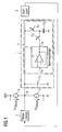
- FIG. 1 shows a control circuit with a switchable bandwidth.
- the control circuit consists of a control unit 1, an actuator 2 and a control system 3.
- a control unit 1 In a point of reference 6 of the control system, two control voltages V1 control, V2 control or respective currents are fed, provided by current sources. 4, 5
- the control device 1 has an integrator acting as first capacitor C1 and an additional device 1 ', the from a voltage follower 7, a second capacitor C2 as well two switches S1, S2 exists.
- the voltage follower 7 has an operational amplifier 71 whose output voltage to the inverting input of the operational amplifier 71 is returned. In this circuit own the Input voltage and the output voltage of the Operational amplifier 71 the same value, i. the Output voltage follows the input voltage, resulting in the Name "voltage follower" justified.
- the system gain is at one.
- the first capacitor C1 is with its first connection to the Reference point 6 connected and with its second connection connected to ground.
- the input 7a of the voltage follower 7 is connected to the first terminal of the first capacitor C1 connected.
- the output 7b of the voltage follower 7 is over one of the switches S2 is connected to the second capacitor C2. Via the further switch S1, the second capacitor C2 switchable parallel to the first capacitor C1.
- the operation of the illustrated control system is like follows. About the one power source 4, the first capacity C1 with a pulsed current applied to a Charging the capacity C1 leads. At the same time the Capacitance C1 via the second current source 5 with another Pulsed current applied, resulting in a discharge of the Capacity C1 leads.
- the capacitance C1 acts as an integrator. If the by the two current sources 4, 5 provided currents are inverse to each other, finds none Discharge or charging the capacity C1 instead and it is a stable condition. Provided by the two Power sources 4, 5 signals provided currents not are inverses to each other, takes a slow Ent- or Charging the capacity C1.
- the voltage follower 7 and the second capacitor C2 are initially ignored.
- the voltage applied to the capacitor C1 represents a manipulated variable of the control system and is supplied to the actuator 2.
- the actuator 2 influences the subsequent controlled system 3.
- the control influenced both by the current sources 4, 5 signals provided control V1, V2 so that they provide control, a controlled variable.
- the system is regulated when the voltage across the capacitor C1 is constant. This is as described achieved when the two signals are control V1, V2 control inverse to each other, that is shifted in phase at the same amplitude and 180 ° and are provided with the opposite sign.
- the switch S1 As long as the second capacitor C2 is not switched on, is the switch S1 is opened. The switch S2 is against closed. This leads to that at the first Capacitance C1 voltage applied by means of voltage follower 7 is tracked to the second capacitor C2. The voltage the second capacitance C2 follows the voltage of the first Capacity C1. When connecting the second capacitor C2 the switch S2 is opened, the switch S1 against it closed. The second capacitor C2 is now with the first Capacitance C1 connected in parallel. This causes the Bandwidth of the control device and thus of the control system decreased overall. It's a slower one Control characteristic before. A connection of the other Capacitance C2 occurs, for example, after a start time ⁇ T, after which the system has settled.
- a suitable Control device (not shown) provided.
- a control device takes one Signal detection (“signal detect”) before and takes place Connecting the further capacity C2 after a presence such signal detection.
- the controlled system described in FIG. 1 can basically be used in any context in which a switchable bandwidth is desired.
- a special preferred application is in the control of signals in optical receiver circuits with an optoelectronic Converter means (eg a photodiode) and a downstream preamplifier.
- Such an optical Receiver circuit of a digital optical receiver is shown in the figure 2.
- a first optoelectronic converter is shown 10 provided in the form of a photodiode, which is an optical Converts information signal into an electrical signal.
- the electrical signal is in a preamplifier 11, 12 amplified and the one input 30a of a post-amplifier 30th (post amplifier) supplied, which is a differential amplifier.
- the preamplifier is preferably one Transimpedance amplifier consisting of a voltage amplifier 11 and a negative feedback resistor 12.
- the im Essentially rectangular output signal of the photodiode 10 becomes a constant current at the input of the preamplifier fixed current source 13 superimposed, which has a suitable offset at the input of the voltage amplifier 11 provides.
- a field effect transistor T1 is provided which is connected in parallel to the negative feedback resistor 12, so that via the at the gate terminal of the transistor T1 voltage applied to the total resistance and thus the Amplitude of the output signal of the preamplifier is set can be.
- a field effect transistor can also be bipolar transistor can be used.
- the Negative feedback resistor can be set in other ways.
- the output signal S MOD of the upper preamplifier 11 and the output signal S MW of the lower preamplifier 21 are supplied to the two inputs 30a, 30b of the post-amplifier 30. Since no optical signal is detected by the photodiode 20, the signal S MW applied to the input 30b has a constant value except for spurious frequencies. In contrast, the signal S MOD represents the rectangular-modulated information signal.
- the current source 23 is regulated in such a way that the signal S MW present at one input 30b of the post-amplifier 30 is just 50% of the signal swing of the useful signal.
- 30 exactly two mutually inverse signals S, -S are generated at the output of the post-amplifier. Otherwise, the output signal is distorted.
- Subsequent components are driven differentially, ie the following components each evaluate the difference between two input signals. Since the signals are inverse to each other, a double amplitude can be evaluated by the following components. This reduces the susceptibility to interference and increases the stability.
- the control device 1 of Figure 1 is integrated.
- the actuator 2 corresponds to the controllable current source 23.
- the controlled system 3 is formed by the preamplifier 21 and the post-amplifier 30.
- the signals V1 and V2 control controlling the Figure 1 are provided by the two output signals S, S of the post-30th With these signals S, -S, the capacitance C1 and after connecting the capacitor C2 and the capacitance C2 is applied.
- the controlled system is adjusted in the event that the two signals S, -S present at the reference point 6 are completely differentially formed. In this case, the voltage across the capacitance C1, C2 is constant.
- the voltage changes at the capacitance and this voltage change is transmitted via the actuator 2 and the controllable current source 23 to the control loop until the signals S, -S at the output of the post-amplifier 30 are inverse to each other or the constant level at the output of the preamplifier 21 is just 50% of the signal swing of the useful signal.
- control device according to the figure 1 only by way of example in the context of the receiver circuit of FIG. 2 has been described. Basically, the control device Can be used wherever switchable bandwidths are required become.
Landscapes
- Physics & Mathematics (AREA)
- Electromagnetism (AREA)
- Engineering & Computer Science (AREA)
- Computer Networks & Wireless Communication (AREA)
- Signal Processing (AREA)
- Amplifiers (AREA)
- Electronic Switches (AREA)
Applications Claiming Priority (4)
| Application Number | Priority Date | Filing Date | Title |
|---|---|---|---|
| US53101103P | 2003-12-19 | 2003-12-19 | |
| US531011P | 2003-12-19 | ||
| US10/817,723 US7421213B2 (en) | 2003-12-19 | 2004-04-02 | Optical receiver control device with a switchable bandwidth |
| US817723 | 2004-04-02 |
Publications (3)
| Publication Number | Publication Date |
|---|---|
| EP1545028A2 true EP1545028A2 (fr) | 2005-06-22 |
| EP1545028A3 EP1545028A3 (fr) | 2005-10-26 |
| EP1545028B1 EP1545028B1 (fr) | 2008-08-06 |
Family
ID=34527149
Family Applications (1)
| Application Number | Title | Priority Date | Filing Date |
|---|---|---|---|
| EP04090494A Expired - Lifetime EP1545028B1 (fr) | 2003-12-19 | 2004-12-17 | Récepteur optique avec dispositif de commande avec un largeur de bande variable |
Country Status (3)
| Country | Link |
|---|---|
| US (2) | US7421213B2 (fr) |
| EP (1) | EP1545028B1 (fr) |
| DE (1) | DE502004007771D1 (fr) |
Cited By (3)
| Publication number | Priority date | Publication date | Assignee | Title |
|---|---|---|---|---|
| AT513104B1 (de) * | 2012-07-10 | 2015-11-15 | Felix Dipl Ing Dr Himmelstoss | Vorrichtung zur Konstanthaltung der Frequenz eines spannungsgesteuerten Oszillators |
| CN112880710A (zh) * | 2021-01-14 | 2021-06-01 | 安徽科达自动化集团股份有限公司 | 光电检测电路及具有其的区间式光电检测器 |
| WO2021151229A1 (fr) * | 2020-01-29 | 2021-08-05 | Stmicroelectronics (China) Investment Co., Ltd | Dispositifs et procédés de détection de communication en champ proche |
Families Citing this family (11)
| Publication number | Priority date | Publication date | Assignee | Title |
|---|---|---|---|---|
| US7421213B2 (en) * | 2003-12-19 | 2008-09-02 | Avago Technologies Limited | Optical receiver control device with a switchable bandwidth |
| JP4569369B2 (ja) * | 2005-04-27 | 2010-10-27 | 住友電気工業株式会社 | 光受信器 |
| JP4928743B2 (ja) * | 2005-06-02 | 2012-05-09 | 株式会社東芝 | 光信号受信回路 |
| US20080002993A1 (en) * | 2006-06-30 | 2008-01-03 | Kirkpatrick Peter E | Optical receiver with dual photodetector for common mode noise suppression |
| CN101355388B (zh) * | 2007-07-25 | 2012-07-04 | 华为技术有限公司 | 接收装置和接收方法 |
| US8541727B1 (en) | 2008-09-30 | 2013-09-24 | Cypress Semiconductor Corporation | Signal monitoring and control system for an optical navigation sensor |
| JP2012231272A (ja) * | 2011-04-26 | 2012-11-22 | Toshiba Corp | 受信回路 |
| US9397385B2 (en) * | 2011-11-09 | 2016-07-19 | Qualcomm Technologies International, Ltd. | Near field communications reader |
| JP2017152776A (ja) * | 2016-02-22 | 2017-08-31 | 技術研究組合光電子融合基盤技術研究所 | 光受信回路 |
| US9960844B1 (en) * | 2017-03-30 | 2018-05-01 | Xilinx, Inc. | Electrically testing an optical receiver |
| US11632174B2 (en) * | 2020-03-13 | 2023-04-18 | Arris Enterprises Llc | Dispersion compensation circuit with cascaded varactor circuit elements |
Family Cites Families (9)
| Publication number | Priority date | Publication date | Assignee | Title |
|---|---|---|---|---|
| US4889985A (en) | 1988-10-26 | 1989-12-26 | Tektronix, Inc. | Combined optical power meter and receiver |
| FI97093C (fi) | 1994-09-09 | 1996-10-10 | Nokia Telecommunications Oy | Nopeasti asettuva vaihelukko |
| US6118399A (en) * | 1998-03-30 | 2000-09-12 | Silicon Laboratories, Inc. | Coarse/fine switching on digital-to-analog conversion output |
| US6476681B1 (en) | 1998-08-11 | 2002-11-05 | Denso International America, Inc. | Adjustable bandwidth phase locked loop with fast settling time |
| JP3775574B2 (ja) * | 2001-05-22 | 2006-05-17 | シャープ株式会社 | 光結合装置 |
| JP3665635B2 (ja) | 2002-11-27 | 2005-06-29 | 株式会社東芝 | 光信号受信回路、及び、光信号受信半導体装置 |
| US7406268B2 (en) * | 2003-08-27 | 2008-07-29 | Avago Technologies Limited | Optical receiver circuit |
| US6952005B2 (en) * | 2003-12-19 | 2005-10-04 | Infineon Technologies Ag | Optical receiver circuit |
| US7421213B2 (en) * | 2003-12-19 | 2008-09-02 | Avago Technologies Limited | Optical receiver control device with a switchable bandwidth |
-
2004
- 2004-04-02 US US10/817,723 patent/US7421213B2/en active Active
- 2004-12-17 EP EP04090494A patent/EP1545028B1/fr not_active Expired - Lifetime
- 2004-12-17 DE DE502004007771T patent/DE502004007771D1/de not_active Expired - Lifetime
-
2008
- 2008-07-28 US US12/180,595 patent/US7792435B2/en not_active Expired - Fee Related
Cited By (5)
| Publication number | Priority date | Publication date | Assignee | Title |
|---|---|---|---|---|
| AT513104B1 (de) * | 2012-07-10 | 2015-11-15 | Felix Dipl Ing Dr Himmelstoss | Vorrichtung zur Konstanthaltung der Frequenz eines spannungsgesteuerten Oszillators |
| WO2021151229A1 (fr) * | 2020-01-29 | 2021-08-05 | Stmicroelectronics (China) Investment Co., Ltd | Dispositifs et procédés de détection de communication en champ proche |
| US12289140B2 (en) | 2020-01-29 | 2025-04-29 | Stmicroelectronics (China) Investment Co., Ltd. | Devices and methods for near-field communication detection |
| CN112880710A (zh) * | 2021-01-14 | 2021-06-01 | 安徽科达自动化集团股份有限公司 | 光电检测电路及具有其的区间式光电检测器 |
| CN112880710B (zh) * | 2021-01-14 | 2022-04-22 | 安徽科达自动化集团股份有限公司 | 光电检测电路及具有其的区间式光电检测器 |
Also Published As
| Publication number | Publication date |
|---|---|
| US20050135817A1 (en) | 2005-06-23 |
| US7792435B2 (en) | 2010-09-07 |
| EP1545028B1 (fr) | 2008-08-06 |
| EP1545028A3 (fr) | 2005-10-26 |
| DE502004007771D1 (de) | 2008-09-18 |
| US20080278228A1 (en) | 2008-11-13 |
| US7421213B2 (en) | 2008-09-02 |
Similar Documents
| Publication | Publication Date | Title |
|---|---|---|
| EP1622257B1 (fr) | Amplificateur pour convertir un signal de courant d'un récepteur optique en un signal de tension | |
| DE69414081T2 (de) | Verstärker mit Offsetgleichspannungskorrektur | |
| DE3213269C2 (fr) | ||
| DE102006047958B4 (de) | Generator für eine exakte Dreieckssignalform | |
| EP1545028B1 (fr) | Récepteur optique avec dispositif de commande avec un largeur de bande variable | |
| DE60217504T2 (de) | Verstärker mit variabler verstärkung für einen offenen regelkreis unter verwendung einer replikatverstärkerzelle | |
| DE4007385A1 (de) | Schaltungsanordnung zum automatischen nullpunkt-abgleich zur behebung von offsetfehlern | |
| DE102014202335A1 (de) | Analog-Digital-Wandler-Schaltung, integrierte Schaltung, elektronisches Gerät und dazugehöriges Verfahren | |
| DE3725339A1 (de) | Automatische justierschaltung zum justieren der zeitkonstanten einer filterschaltung | |
| EP1545029B1 (fr) | Dispositif de réception optique | |
| WO2005046094A1 (fr) | Procede et systeme pour convertir une serie d'impulsions de reception optiques en une serie d'impulsions de sortie electriques | |
| DE10247133B4 (de) | Gesteuerte Stromquelle, insbesondere für Digital-Analog-Umsetzer in zeitkontinuierlichen Sigma-Delta-Modulatoren | |
| EP1171981A1 (fr) | Filtre gmsk numerique | |
| EP1587214B1 (fr) | Circuit pour commander un paramètre d'un signal électrique | |
| DE69827368T2 (de) | Ausgangsstufe mit selbstregelnder anstiegszeitsteuerung | |
| EP0977406B1 (fr) | Circuit de transmission de signaux numériques avec séparation galvanique | |
| DE102006026906B4 (de) | Schaltung und Verfahren zur Pulsweitenmodulation mittels synchronisierter, selbstoszillierender Pulsweitenmodulatoren | |
| DE102005041052B3 (de) | Verfahren zur Stabilitätskontrolle einer selbstschwingenden Treiberschaltung und selbstschwingende Treiberschaltung | |
| DE3015806C2 (de) | Schaltungsanordnung zur Abnahme von Signalen von Halbleiter-Bild- oder -Zeilensensoren | |
| DE102005062449A1 (de) | Optischer Empfänger | |
| EP0263416B1 (fr) | Circuit électronique de parole | |
| DE69920404T2 (de) | Telefonempfangsschaltung zur Unterdrückung der Schaltungsinterferenz | |
| EP1116330B1 (fr) | Circuit differentiel d'entree pour systeme de traitement numerique des signaux | |
| EP0735679B1 (fr) | Détecteur de pente | |
| DE2545870A1 (de) | Schaltungsanordnung fuer einen delta- modulator mit automatischer geraeuschsperre und automatischer verstaerkungsregelung |
Legal Events
| Date | Code | Title | Description |
|---|---|---|---|
| PUAI | Public reference made under article 153(3) epc to a published international application that has entered the european phase |
Free format text: ORIGINAL CODE: 0009012 |
|
| AK | Designated contracting states |
Kind code of ref document: A2 Designated state(s): AT BE BG CH CY CZ DE DK EE ES FI FR GB GR HU IE IS IT LI LT LU MC NL PL PT RO SE SI SK TR |
|
| AX | Request for extension of the european patent |
Extension state: AL BA HR LV MK YU |
|
| PUAL | Search report despatched |
Free format text: ORIGINAL CODE: 0009013 |
|
| AK | Designated contracting states |
Kind code of ref document: A3 Designated state(s): AT BE BG CH CY CZ DE DK EE ES FI FR GB GR HU IE IS IT LI LT LU MC NL PL PT RO SE SI SK TR |
|
| AX | Request for extension of the european patent |
Extension state: AL BA HR LV MK YU |
|
| RIC1 | Information provided on ipc code assigned before grant |
Ipc: 7H 04B 10/158 A Ipc: 7H 03L 7/00 B |
|
| 17P | Request for examination filed |
Effective date: 20060227 |
|
| AKX | Designation fees paid |
Designated state(s): DE FR GB |
|
| 17Q | First examination report despatched |
Effective date: 20060929 |
|
| RTI1 | Title (correction) |
Free format text: OPTICAL RECEIVER WITH A CONTROL DEVICE WITH VARIABLE BANDWIDTH |
|
| GRAP | Despatch of communication of intention to grant a patent |
Free format text: ORIGINAL CODE: EPIDOSNIGR1 |
|
| RAP1 | Party data changed (applicant data changed or rights of an application transferred) |
Owner name: AVAGO TECHNOLOGIES FIBER IP (SINGAPORE) PTE. LTD. |
|
| GRAS | Grant fee paid |
Free format text: ORIGINAL CODE: EPIDOSNIGR3 |
|
| GRAA | (expected) grant |
Free format text: ORIGINAL CODE: 0009210 |
|
| AK | Designated contracting states |
Kind code of ref document: B1 Designated state(s): DE FR GB |
|
| REG | Reference to a national code |
Ref country code: GB Ref legal event code: FG4D Free format text: NOT ENGLISH |
|
| REF | Corresponds to: |
Ref document number: 502004007771 Country of ref document: DE Date of ref document: 20080918 Kind code of ref document: P |
|
| PLBE | No opposition filed within time limit |
Free format text: ORIGINAL CODE: 0009261 |
|
| STAA | Information on the status of an ep patent application or granted ep patent |
Free format text: STATUS: NO OPPOSITION FILED WITHIN TIME LIMIT |
|
| 26N | No opposition filed |
Effective date: 20090507 |
|
| REG | Reference to a national code |
Ref country code: FR Ref legal event code: ST Effective date: 20090831 |
|
| PG25 | Lapsed in a contracting state [announced via postgrant information from national office to epo] |
Ref country code: FR Free format text: LAPSE BECAUSE OF NON-PAYMENT OF DUE FEES Effective date: 20081231 |
|
| REG | Reference to a national code |
Ref country code: DE Ref legal event code: R082 Ref document number: 502004007771 Country of ref document: DE Representative=s name: DILG HAEUSLER SCHINDELMANN PATENTANWALTSGESELL, DE |
|
| REG | Reference to a national code |
Ref country code: DE Ref legal event code: R082 Ref document number: 502004007771 Country of ref document: DE Representative=s name: DILG HAEUSLER SCHINDELMANN PATENTANWALTSGESELL, DE Effective date: 20130625 Ref country code: DE Ref legal event code: R081 Ref document number: 502004007771 Country of ref document: DE Owner name: AVAGO TECHNOLOGIES GENERAL IP (SINGAPORE) PTE., SG Free format text: FORMER OWNER: AVAGO TECHNOLOGIES FIBER IP (SINGAPORE) PTE. LTD., SINGAPORE, SG Effective date: 20130625 |
|
| REG | Reference to a national code |
Ref country code: GB Ref legal event code: 732E Free format text: REGISTERED BETWEEN 20130725 AND 20130731 |
|
| PGFP | Annual fee paid to national office [announced via postgrant information from national office to epo] |
Ref country code: GB Payment date: 20151125 Year of fee payment: 12 |
|
| GBPC | Gb: european patent ceased through non-payment of renewal fee |
Effective date: 20161217 |
|
| PG25 | Lapsed in a contracting state [announced via postgrant information from national office to epo] |
Ref country code: GB Free format text: LAPSE BECAUSE OF NON-PAYMENT OF DUE FEES Effective date: 20161217 |
|
| REG | Reference to a national code |
Ref country code: DE Ref legal event code: R081 Ref document number: 502004007771 Country of ref document: DE Owner name: AVAGO TECHNOLOGIES INTERNATIONAL SALES PTE. LT, SG Free format text: FORMER OWNER: AVAGO TECHNOLOGIES GENERAL IP (SINGAPORE) PTE. LTD., SINGAPORE, SG Ref country code: DE Ref legal event code: R082 Ref document number: 502004007771 Country of ref document: DE Representative=s name: DILG, HAEUSLER, SCHINDELMANN PATENTANWALTSGESE, DE Ref country code: DE Ref legal event code: R082 Ref document number: 502004007771 Country of ref document: DE Representative=s name: DILG HAEUSLER SCHINDELMANN PATENTANWALTSGESELL, DE |
|
| PGFP | Annual fee paid to national office [announced via postgrant information from national office to epo] |
Ref country code: DE Payment date: 20211210 Year of fee payment: 18 |
|
| REG | Reference to a national code |
Ref country code: DE Ref legal event code: R119 Ref document number: 502004007771 Country of ref document: DE |
|
| PG25 | Lapsed in a contracting state [announced via postgrant information from national office to epo] |
Ref country code: DE Free format text: LAPSE BECAUSE OF NON-PAYMENT OF DUE FEES Effective date: 20230701 |