EP1545046B1 - Verbesserungen für Datenrückgewinnungsschaltungen mit Überabtastung zu Wahl des besten Datenabtastwertes - Google Patents
Verbesserungen für Datenrückgewinnungsschaltungen mit Überabtastung zu Wahl des besten Datenabtastwertes Download PDFInfo
- Publication number
- EP1545046B1 EP1545046B1 EP20040105473 EP04105473A EP1545046B1 EP 1545046 B1 EP1545046 B1 EP 1545046B1 EP 20040105473 EP20040105473 EP 20040105473 EP 04105473 A EP04105473 A EP 04105473A EP 1545046 B1 EP1545046 B1 EP 1545046B1
- Authority
- EP
- European Patent Office
- Prior art keywords
- data
- selection
- edge
- bits
- logic level
- Prior art date
- Legal status (The legal status is an assumption and is not a legal conclusion. Google has not performed a legal analysis and makes no representation as to the accuracy of the status listed.)
- Expired - Lifetime
Links
- 238000011084 recovery Methods 0.000 title claims description 25
- 230000015654 memory Effects 0.000 claims description 33
- 238000000034 method Methods 0.000 claims description 18
- 238000003708 edge detection Methods 0.000 claims description 15
- 230000007704 transition Effects 0.000 claims description 15
- 238000005070 sampling Methods 0.000 claims description 13
- 238000010200 validation analysis Methods 0.000 claims description 12
- 238000004891 communication Methods 0.000 claims description 10
- 230000009467 reduction Effects 0.000 claims description 4
- 230000001360 synchronised effect Effects 0.000 claims description 4
- 238000010586 diagram Methods 0.000 description 13
- 230000008569 process Effects 0.000 description 5
- 238000012549 training Methods 0.000 description 5
- 230000000694 effects Effects 0.000 description 4
- 230000008901 benefit Effects 0.000 description 3
- 230000007423 decrease Effects 0.000 description 3
- 238000004364 calculation method Methods 0.000 description 2
- 230000008859 change Effects 0.000 description 2
- 230000007246 mechanism Effects 0.000 description 2
- 230000000630 rising effect Effects 0.000 description 2
- 238000012935 Averaging Methods 0.000 description 1
- 238000010276 construction Methods 0.000 description 1
- 238000001514 detection method Methods 0.000 description 1
- 238000005516 engineering process Methods 0.000 description 1
- 238000004519 manufacturing process Methods 0.000 description 1
- 238000012545 processing Methods 0.000 description 1
- 230000004044 response Effects 0.000 description 1
Images




Classifications
-
- H—ELECTRICITY
- H04—ELECTRIC COMMUNICATION TECHNIQUE
- H04L—TRANSMISSION OF DIGITAL INFORMATION, e.g. TELEGRAPHIC COMMUNICATION
- H04L7/00—Arrangements for synchronising receiver with transmitter
- H04L7/02—Speed or phase control by the received code signals, the signals containing no special synchronisation information
- H04L7/033—Speed or phase control by the received code signals, the signals containing no special synchronisation information using the transitions of the received signal to control the phase of the synchronising-signal-generating means, e.g. using a phase-locked loop
- H04L7/0337—Selecting between two or more discretely delayed clocks or selecting between two or more discretely delayed received code signals
Definitions
- the present invention relates to high speed serial communications/data transfers between integrated circuits or systems and more particularly to a method and circuit for implementing the best data sample selection in a data recovery circuit based on an oversampling technique when the incoming data stream suffers of jitter and is skewed with respect to the reference clock.
- FIG. 1 shows a typical eye diagram for a high speed serial data link.
- Data jitter or phase error (skew) between clock and data thus significantly reduce the useful sampling window.
- the reliable sampling window hatchched area
- circuit process deviations, operating temperature and power supply variations can also have a negative impact on sampling window width and thus on the targeted circuit accuracy.
- the selection of the best sample generally relies on a training pattern specific to the data communication protocol in consideration.
- the training pattern is used during a calibration step to determine which clock phase is the best to recover the data and this calibration step is repeated whenever required.
- a data recovery circuit built for a given communication data protocol is generally not suitable to recover data sent using a different data communication protocol as it will be unable to recognize the training pattern and thus to select the best data sample.
- the duration of said training patterns is relatively short compared to the data duration and therefore are not representative of the jitter affecting the data.
- a plurality of over sampled signals (SO, ... , S.sub.n-1) is obtained by over sampling an incoming serial binary data (bits) stream with the n phases (C.sub.0, ... , C.sub.n-1) of a multiphase clock signal.
- a reliable over sampled signal is selected according to a select signal (G.sub.0... , G.sub.n-1) generated by an edge detector which designates which over sampled signal is the best for subsequent processing.
- the circuit comprises a plurality of n substantially identical logic blocks.
- the first logic block includes a latch receiving sampled signal So on its data input and the phase clock signal C.sub.0 on its clock input.
- Each other logic block e.g.
- logic block i further includes a multiplexer having two inputs, the first input is connected to the output of the latch of the preceding logic block and the second input receives sampled signal S.sub.i.
- the multiplexer is controlled by a signal which is either G.sub.1 or the control signal of the following multiplexer.
- the output of the multiplexer is connected to the data input of the latch, the clock input of which receives clock signal C.sub.i.
- the output of the latch in the last logic block is connected to the clock input of an output latch, the clock input of which is coupled to a phase in opposition with phase C.sub.n-1.
- the output latch stores the recovered data during a full clock period.
- US 6,584,163 discloses a shared data and clock recovery circuit including a clock synthesizer for generating sampling signals having different phases, a multiple transition detector for receiving a data stream and sampling signals, and for detecting edges in a data stream in response to the sampling signals, a counter and accumulator for detecting the time occurrences and total number of edges, and for performing weighted average calculation to select one of the phases, a decision circuit for detecting the phase difference between a source clock and a local clock such that if the PPM difference between the source clock and the local clock is at least 200 PPM, then selection of a phase is based upon stored historical information, and if the PPM difference between the source clock and the local clock is less than 200 PPM, then selection of a phase is based on a weighted averaging calculation. Consequently, there is a real need for an improved data recovery circuit that would be independent of any data communication protocol and capable to support jitter undesirable effects and skew, i.e. the phase difference between any data link signal and an
- DR data recovery
- the data to recover is first oversampled using the multiple phases of a reference clock to generate a set of data samples.
- An edge detection circuit is used to locate the position of edges in the set of data samples.
- a data edge memory memorizes the bit edge positions.
- a selection determination circuit provides selection signals to indicate which data sample is the farthest from the bit edges.
- a selection validation circuit validates the selection signals to avoid any false determination in said selection signals. Validated selection signals are stored in a selection memory.
- a data sample selection circuit processes both the data samples and the memorized validated selection signals to determine which data sample is the best candidate to recover the data.
- the performance of a data recovery circuit being tied to its jitter tolerance, the improved DR circuit that is able to store the position of data edges over a long period of time, can therefore take into account the data jitter to select the best sample.
- the choice of the best data sample only depends on data transitions, the improved DR circuit does not rely on any training pattern and thus is totally independent of the data communication protocol.
- the data recovery mechanism of the present invention is also independent of the number of data links.
- the improved data recovery circuit 10 first includes a multiple phase generator 11 driven by a reference clock synchronized with the data link.
- the multiphase clock generator 11 is required to generate an adequate number n of clock phases, e.g. 16 in the present implementation, referenced C 1 to C 16 , that are derived from a reference clock labeled clk.
- Said multiple phases are applied to an oversampling circuit 12 (and to other circuits whenever necessary) that receives the stream of serial data to recover at the In terminal to generate data samples, referenced D 1 to D 16 . It further includes an edge detection circuit 13, a data edge memory 14, a selection determination circuit 15, a selection validation circuit 16, and a selection memory 17 that are connected in series. Control logic circuit 18 plays the role of a state machine vis à vis some blocks. Logic circuits and memories 13 to 18 form the so-called decision circuit referenced 20. Finally, the data samples D 1 to D 16 and the signals MVS 1 to MVS 16 output by the selection memory 17 are applied to data selection circuit 19.
- the incoming stream of serial data is continuously oversampled in oversampling circuit 12 by means of said multiple phases of the reference clock.
- Each data sample is compared in edge detector circuit 13 to the data sample collected with the next adjacent clock phase to determine the presence of a data edge or transition and the edge information i.e. the edge positions, is collected in data edge memory 14 for a duration that can be tuned.
- This data edge memory 14 can be cleared at regular time intervals. Tuning and clearing are performed by control logic circuit 18.
- the selection determination circuit 15 uses the memorized edge information to indicate which data sample is the farthest from the data edges.
- Selection validation circuit 16 has the key role of validating the selection to avoid false determination due to jitter and skew.
- the validated values of the selection signals are memorized in selection memory 17, so that these values can be used while new data edges are processed and new selection signals are updated. Finally, the memorized validated selection signals MVS 1 to MVS 16 and the data samples D 1 to D 16 are exploited in data selection circuit 19 to recover the data. As apparent in FIG. 2 , the recovered data RD is available at the Out terminal.
- Block 20 which is composed of a plurality of logic circuits and memories will be referred to hereafter as the decision circuit. The decision circuit is thus based on the detection of data edges or transitions in the set of data samples to drive the data sample selection circuit 19 in order to select the best sample to be kept, i.e. the recovered data RD.
- the clock frequency can be the same as the data frequency, i.e. one data bit per clock period or half of the data frequency, i.e. two data bits per clock period, also referred to as single data rate (SDR) or double data rate (DDR) respectively.
- the reference clock may be synchronously transmitted by the distant apparatus or may be recovered from the data stream using standard clock recovery circuits.
- a conventional PLL based multiphase clock generator is shown in FIG. 3 where it bears numeral 11. Now turning to FIG.
- the reference clock signal clk and the loop signal that is internally generated by the PLL circuit 11 are applied to the phase comparator 21, which in turn generates a signal that is supplied to a charge pump 22.
- the latter outputs a controlled signal that is fed to a voltage controlled oscillator (VCO) circuit 24 via a loop filter 23.
- VCO voltage controlled oscillator
- the VCO circuit 24 is coupled to a frequency divider 25 that supplies said loop signal on line 26.
- the desired number N of oversampling clock phases, sixteen in the instant case, obtained either on the rising edge or the falling edge of the reference clock, are referenced C 1 to C 16 .
- the oversampling circuit 12 collects either one bit (SDR) or two consecutive bits (DDR in sixteen samples. The sampling is done on each phase C 1 to C 16 .
- An example of a simple implementation of oversampling circuit 12 is shown in FIG. 4 .
- oversampling circuit 12 includes 16 flip-flops 27-1 to 27-16 that are respectively controlled by the sixteen phases C 1 to C 16 .
- D 1 to D 16 represent the 16 data samples available at the output of their respective flip-flop.
- the edge detection circuit 13 is directly connected at the oversampling circuit 12 output and is responsible to detect a value change between two consecutive data samples.
- the edge detection circuit 13 is made of 16 edge detection elements, each one corresponding to a data sample.
- edge detection element EDi it consists of a XOR gate 28-i that compares the two consecutive data samples Di and Di+1.
- the comparison result Ei i.e. the edge information
- Ci clock phase
- the edge detection element output switches to the '1' level during a single clock period.
- the edge information is collected during an extended period of time so that the data jitter with regards to oversampling clock phases is taken into account.
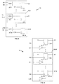
- the data edge memory block 14 is directly connected at the edge detection circuit 13 output. Now turning to FIG. 6 , the data edge memory block 14 is made of 16 data edge memory elements, each one corresponding to a data sample. Thus, there are as many data edge memory elements as there are edge detection elements.
- the data edge memory block 14 is a first key feature of the present invention. Let us consider data edge memory element DEMi, it mainly consists of an asynchronous reset flip-flop (or a similar register element) 30-i which has its data input permanently set to '1' and its clock input connected to a reset signal RC.
- the RC clock signal generated by the control logic circuit 18, is a pulse used to reset periodically every data edge memory elements at the '1' value.
- the RC signal period or edge sampling period is tuned in a configuration register (not shown).
- the edge information signal Ei is applied to the asynchronous input via an inverter 31-i.
- any edge information signal Ei at the '1' level i.e. indicating the presence of a data edge, sets a '0' level in the corresponding flip-flop 30-i.
- the signal latched in flip-flop 30-i, labeled E'i, at this '0' level, is kept for an extended length of time such as several tenths or hundreds of clock periods.
- One advantage of using an asynchronous reset flip-flop is that it allows to collect data edge events during such an extended period of time very simply, however, other implementations could be envisioned as well.
- Another advantage is that it collects the edge information independently of their related oversampling clock phase. As a significant result, all signals derived therefrom could be exploited with a determined oversampling clock phase, e.g. C 1 .
- sixteen phases of a reference clock are thus used to collect sixteen data samples during each clock period.
- the selection determination circuit 15 is directly connected at the data edge memory block 14 output and has the essential role of determining which data sample(s) is (are) to be kept. In essence, it uses the memorized edge information to indicate which sample is the farthest from the data edges. At the input of this circuit, the edge information is thus presented under the form of a bit map with as many bits as there are samples.
- the selection determination circuit locates the edges of the zone(s) filled with '1's and progressively reduces the width of the zone until it only contains only one '1's. As this width reduction is performed alternatively on each side, then the remaining '0' points to the center of the zone where none data edge was located, i.e. it points to the data sample which is the farthest from the data edge position.
- the particular pattern 110 is searched in the suite of the E' values to locate the right side of a zone filled with '1's.
- the right most value of the suite of the E' values (E' 16 in this preferred implementation) is considered to be adjacent with the leftmost value of the suite of E' value (i.e. E' 1 ).
- E' 1 the leftmost value of the suite of E' value
- the second step of the algorithm searches for the 011 pattern which is characteristic of the left side of a zone filled with '1's in the suite of E' values.
- the leftmost value of the suite of the E' values (E' 1 in the preferred implementation) is considered to be adjacent with the rightmost value of the suite of E' values (i.e. E' 16 ).
- E' 1 the leftmost value of the suite of the E' values
- E' 16 the rightmost value of the suite of E' values
- FIG. 7 shows a preferred hardware implementation of the above described algorithm that functionally performs these operations.
- flip-flop 30-i collects the edge information using its asynchronous reset input.
- the selection signal Start of selector 32-i (delivered by the control logic circuit 18) switches to the '1' level during one clock period and then returns to '0'.
- flip-flop 30-i can be synchronously set to '1' by having its clock input switching to '1' then back to '0'.
- the signal at the output of the selector 32-i is combined using NAND, AND and INVERTER gates to execute the two steps of the above described algorithm.
- Fi-1 is combined in a NAND gate with the inverted F value of the next SD element (SDi+1), i.e. Fbi+1.
- SDi+1 next SD element
- Fbi+1 next SD element
- the resulting signal is then ANDed with the Fi signal to form the Gi signal, thus effectively detecting the occurrence of the 110 pattern and forcing the middle '1' to a '0' when the pattern is found.
- the Gi signal is combined with the G signal from adjacent SD element to detect the 011 pattern and replace the middle value thereof by a '0' when this pattern is found.
- the Hi signal is captured in flip-flop 38-i at each clock phase C 1 rising edge to generate selection signal Si.
- the maximum number of iterations to be performed is equal to the fourth of the number of data samples in the case of DDR data (i.e. four iterations in the preferred implementation using sixteen samples per clock period) or one half of the number of data samples in the case of SDR data (i.e. eight iterations in the case of the preferred implementation).
- FIG. 7 illustrates the assembly of 16 SD elements to build the totality of the selection determination circuit 15.
- the selection signals S(1:16) cannot be directly used to select the best data sample(s) to be kept as their values is subject to change between the different iterations. However, given the condition that the data edge collection delay in memory 14 is always greater than the iteration delay in circuit 15, the selection signals S(1:16) values are stored in a memory at the same time or just before taking new data edges are processed.
- FIG. 8 shows a preferred implementation of the innovative selection validation circuit 16 of FIG. 2 which is another key feature of the present invention, because it has the essential role of validating the selection.
- a group of four four-way AND gates referenced 41-1 to 41-4 processes the selection signals S 1 to S 16 , four per four.
- the outputs of these four AND gates are connected to the respective inputs of four-way NAND gate 42.
- the signal that is output from NAND gate 42 is applied to a first input of a battery of 16 two-way AND gates referenced 43-1 to 43-16.
- the respective selection signal is applied on the second input of each of these two-way AND gates, for instance selection signal S 1 is applied to AND gate 43-1 to generate signal VS 1 and so on.
- the selection determination circuit 15 will incorrectly indicate that each data sample is to be recovered by setting each selection signal S(1:16) to the '1' level.
- the selection validation circuit 16 disable all selection signals when they all are at the '1' level. As apparent in FIG. 8 , selection signals S 1 to S 16 are ANDed in two steps, first in AND gates 41-1 to 41-4, then in NAND gates 42 for technology reasons. As a result, NAND gate 42 output is at '1', if at least one selection signal is at '0' and at '0' otherwise. This output is then used as the validation signal for the selection signals S 1 to S 16 .
- VS 1 to VS 16 designate the selection signals that have been validated. It is remarkable to notice that the determination of the best selection signals and their validation performed in circuits 15 and 16 only imply the use of only combinatorial logic instead of complex computation means such as a microprocessor.
- Selection memory block 17 can have a similar construction to the data edge memory block 14.
- selection memory element SMi which simply consists of asynchronous reset flip-flop 30'-i
- the validated signal VSi is applied to its asynchronous input and its clock input connected to the reset signal RC.
- the signal latched in flip-flop 30'-i, labeled MVSi is kept for an extended length of time such as several tenths or hundreds of the reference clock period.
- the memorized validated selection signals in flip-flops 30'-1 to 30'-16 are labeled MVS 1 to MVS 16 respectively.
- the data sample selection circuit 19 is depicted in FIG. 10 . It first includes four groups of four two-way AND gates referenced 44-1 to 44-16. In each group, the output of the four AND gates is connected to one input of a four-way OR gate. As apparent in FIG. 10 , these OR gates are referenced 45-1 to 45-4. The outputs of OR gates 45-1 and 45-2 are connected to an input of a two-way OR gate 46-1. Likewise, the outputs of OR gates 45-3 and 45-4 are connected to an input of a two-way OR gate 46-2. The output of OR gate 46-1 is connected to the data input of flip-flop 47-1 whose clock input receives clock phase C 1 .
- OR gate 46-2 is connected to the data input of flip-flop 47-2 whose clock input receives clock phase C 9 (in phase opposition with clock phase C 1 ).
- Signals latched in flip-flops 47-1 and 47-2 are applied to two-way OR gate 48, the output of which is connected to the data input of flip-flop 49. Its clock input is driven by clock phase C 1 .
- the signal latched in flip-flop 49 is the recovered data RD.
- the data selection circuit 19 shown in FIG. 10 illustrates how the memorized selection signals are exploited to recover the data. The best data sample is selected using AND gates (or AND-OR gates). The different combinations are then further combined using OR gates.
- the OR gate 48 then combines the data coming from flip-flops 47-1 and 47-2 and the recovered data RD is captured by the C 1 clock phase.
- the improved data recovery circuit 10 schematically shown in FIG. 2 is very simple and do not require high speed performance.
- the disclosed method is based on collecting all data edges, then locating the edges in the sampling window in the eye diagram and finally locating the zone of stable data where the data can be safely recovered.
- the disclosed method allows to take into account the random data jitter. Because it is only based on data edge detection, it is does not depend on the data communication protocol that is used.
Landscapes
- Engineering & Computer Science (AREA)
- Computer Networks & Wireless Communication (AREA)
- Signal Processing (AREA)
- Synchronisation In Digital Transmission Systems (AREA)
Claims (7)
- Datenrückgewinnungs-Schaltung (10) zum Wiederherstellen der besten Abtastung in einem Satz von Datenabtastungen, die durch Überabtasten der wiederherzustellenden Daten in einem eingehenden Strom von Datenbits erhalten wurden, wobei die Datenrückgewinnungs-Schaltung das Folgende umfasst:einen Dateneingang (In) zum Empfangen des eingehenden Stroms von Datenbits (DD), der seriell auf einer Datenübertragungsverbindung hoher Geschwindigkeit mit Jitter und Phasenverschiebung bei einer vorgegebenen Datenrate synchron mit einem Referenztakt übertragen wurde;ein Überabtastungsmittel (12), das mit dem Dateneingang verbunden ist, zum Abtasten der Datenbits, um die n Phasen (C1, ... Cn) des Referenz-Taktsignals (clk), das mit einem Mehrphasen-Taktgenerator (11) erzeugt wurde, wiederherzustellen und einen Satz von Datenabtastungen (D1, ..., Dn) während jeder Referenztakt-Periodendauer zu erzeugen;ein Flanken-Erkennungsmittel (13), das mit den Überabtastungsmitteln verbunden ist, um wenigstens zwei aufeinanderfolgende Datenabtastungen zu vergleichen und einen entsprechenden Satz von Signalen (E1, ..., En) zu erzeugen, die die Flankendaten zum Kennzeichnen der Datenflanken- oder -Übergangsposition wiedergeben, sodass beim Erkennen einer Datenflanke zwischen den wenigstens zwei aufeinanderfolgenden Datenabtastungen das Datenflanken-Informationssignal einen vorbestimmten binären Logikpegel und ansonsten den entgegensetzten binären Logikpegel annimmt;wobei die Datenrückgewinnungs-Schaltung das Folgende umfasst:ein erstes Speichermittel (14), das mit den Flankenerkennungsmitteln verbunden ist, um die Datenflanken-Informationen in einem entsprechenden Satz von Signalen (E'1, ..., E'n) zusammenzuführen, die in der Form eines n-Bit-Abbildes (map of n bits) für eine Vielzahl von Taktzyklen dargestellt werden, wobei das Datenflanken-Informationssignal einen ersten binären Logikpegel und ansonsten einen zweiten binären Logikpegel annimmt und die letzte Position des Bit-Abbildes als benachbart zu der ersten Position des Bit-Abbildes und umgekehrt betrachtet wird;Auswahl-Festlegungsmittel (15), die mit den ersten Speichermitteln verbunden sind, um die gespeicherten Datenflanken-Informationssignale zum Erzeugen von Auswahlsignalen (S1, ..., Sn) zu verwenden, indem der mit den Binärwerten, die den zweiten binären Logikpegel in dem Bit-Abbild wiedergeben, gefüllte Bereich ermittelt und seine Breite durch das Ausführen aufeinanderfolgender Iterationen abwechselnd an den beiden Seiten des Bereichs verringert wird, bis er nur einen Wert bei dem zweiten binären Logikpegel enthält, der auf den Mittelpunkt des Bereichs verweist, an dem keine Datenflanke ermittelt wurde, wodurch das Auswählen der entsprechenden Datenabtastung ermöglicht wird, die von den Datenflanken-Positionen am weitesten entfernt ist;Auswahl-Bestätigungsmittel (16), die mit den Auswahl-Festlegungsmitteln verbunden sind, um die Auswahlsignale mittels dem Erzeugen von bestätigten Auswahlsignalen (VS1, ..., VSn) nur in einem Fall, in dem die n Bits des Bit-Abbildes nicht alle denselben Wert aufweisen, zu bestätigen, um eine falsche Ermittlung aufgrund von Jitter/Phasenverschiebung zu vermeiden.zweite Speichermittel (17), die mit dem Auswahl-Prüfmitteln verbunden sind, zum Speichern der bestätigten Werte des Auswahlsignale in einem entsprechenden Satz von Signalen (MVS1, ..., MVSn) ; undDatenabtast-Auswahlmittel (19), die mit den Überabtastmitteln zum Empfangen der Datenabtastungen (D1, ..., Dn) und mit den zweiten Speichermitteln zum Empfangen der gespeicherten Werte der bestätigten Auswahlsignale (MVS1, ..., MVSn) und zum Erzeugen der wiederhergestellten Daten (RD) unter Verwendung der Datenabtastungen und der gespeicherten Werte verbunden sind.
- Daten-Rückgewinnungsschaltung nach Anspruch 1, wobei in der Auswahl-Festlegungsschaltung die Verringerung an einer Menge von drei aufeinanderfolgenden Bits ausgeführt wird.
- Daten-Rückgewinnungsschaltung nach Anspruch 2, wobei es sich bei dem ersten bzw. zweiten Logikpegel um 0 bzw. 1 handelt und es sich bei der Verringerung auf der linken Seite des Bit-Abbildes bei der Menge von drei aufeinanderfolgenden Bits um 110, was in 100 umgeformt wird und, und bei der Verringerung auf der rechten Seite des Bit-Abbildes bei der Menge von drei aufeinanderfolgenden Bits um 011 handelt, was in 001 umgeformt wird.
- Verfahren zum Wiederherstellen der Daten in einem eingehenden Datenstrom mit Jitter und Phasenverschiebung in Bezug auf einen Referenztakt, indem die beste Datenabtastung in einem Satz von Datenabtastungen ausgewählt wird, der durch Überabtasten des eingehenden Datenstroms erhalten wurde, wobei das Verfahren die folgenden Schritte umfasst:Überabtasten des eingehenden Datenstroms mit den n Phasen des Referenztaktes, um einen Satz von n Datenabtastungen zu erzeugen;Ermitteln der Position der Datenflanken oder -übergänge in dem Satz von Datenabtastungen und Erzeugen eines n-Bit-Abbildes, wobei die n Bits Flankenpositionen wiedergeben, indem ein ermittelter binärer Logikwert den Datenflanken-Positionen und andernfalls der entgegengesetzten Wert zugewiesen wird;Speichern des n-Bit-Abbildes, worin sich die Bits einen ersten binären Logikpegel für ermittelte Datenflanken und andernfalls einen zweiten binären Logikpegel annehmen und worin die letzte Bit-Abbildes als benachbart zu der ersten Position des Bit-Abbildes betrachtet wird und umgekehrt;wobei das Verfahren dadurch gekennzeichnet ist, dass es ferner die folgenden Schritte umfasst:Auffinden des Bereichs, der mit Binärwerten gefüllt ist, die den zweiten Logikpegel in dem Bit-Abbild wiedergeben, und Verringern seiner Breite durch das aufeinanderfolgendes Ausführen von Iterationen abwechselnd auf den beiden Seiten des Bereichs, bis er nur einen Wert bei dem zweiten Logikpegel enthält, der auf die Mitte des Bereichs verweist, wo keine Datenflanke ermittelt wurde, wodurch ermittelt wird, welche Datenabtastung am weitesten von den Datenflanken entfernt ist, d.h., bei welcher Datenabtastung es sich um den besten Kandidaten für die wiederherzustellenden Daten handelt;Bestätigen der Auswahlsignale durch das Erzeugen bestätigter Auswahlsignale nur in einem Fall, bei dem die n Bits des Bit-Abbildes nicht alle denselben Wert aufweisen, um eine falsche Ermittlung wegen Jitter und Phasenverschiebung zu vermeiden;Speichern der bestätigten Auswahlsignale; undVerwenden der gespeicherten bestätigten Auswahlsignale und der Datenabtastungen zum Auswählen der besten Datenabtastung, um die wiederhergestellten Daten wiederzugeben.
- Verfahren nach Anspruch 4, wobei das Bit-Abbild während mehreren Referenztakt-Perioden gespeichert wird.
- Verfahren nach Anspruch 4, wobei die Ermittlung das Vergleichen von zwei aufeinanderfolgenden Datenabtastungen und das Erzeugen eines entsprechenden Signalsatzes umfasst, der die Datenflanken-Informationen enthält, d.h. die Positionen der Datenflanken, sodass beim Erkennen eines Übergangs zwischen zwei aufeinanderfolgenden Datenabtastungen das Signal einen ersten Logikpegel (z.B. '1') und ansonsten einen zweiten Logikpegel (z.B. '0') annimmt.
- Verfahren nach Anspruch 4, wobei das Überabtasten unter Verwendung der mehreren Phasen eines Referenztaktes ausgeführt wird.
Priority Applications (1)
| Application Number | Priority Date | Filing Date | Title |
|---|---|---|---|
| EP20040105473 EP1545046B1 (de) | 2003-12-19 | 2004-11-03 | Verbesserungen für Datenrückgewinnungsschaltungen mit Überabtastung zu Wahl des besten Datenabtastwertes |
Applications Claiming Priority (3)
| Application Number | Priority Date | Filing Date | Title |
|---|---|---|---|
| EP33681248 | 2003-12-19 | ||
| EP03368124 | 2003-12-19 | ||
| EP20040105473 EP1545046B1 (de) | 2003-12-19 | 2004-11-03 | Verbesserungen für Datenrückgewinnungsschaltungen mit Überabtastung zu Wahl des besten Datenabtastwertes |
Publications (3)
| Publication Number | Publication Date |
|---|---|
| EP1545046A2 EP1545046A2 (de) | 2005-06-22 |
| EP1545046A3 EP1545046A3 (de) | 2006-11-22 |
| EP1545046B1 true EP1545046B1 (de) | 2009-01-14 |
Family
ID=34524772
Family Applications (1)
| Application Number | Title | Priority Date | Filing Date |
|---|---|---|---|
| EP20040105473 Expired - Lifetime EP1545046B1 (de) | 2003-12-19 | 2004-11-03 | Verbesserungen für Datenrückgewinnungsschaltungen mit Überabtastung zu Wahl des besten Datenabtastwertes |
Country Status (1)
| Country | Link |
|---|---|
| EP (1) | EP1545046B1 (de) |
Families Citing this family (2)
| Publication number | Priority date | Publication date | Assignee | Title |
|---|---|---|---|---|
| WO2009141680A1 (en) * | 2008-05-19 | 2009-11-26 | Freescale Semiconductor, Inc. | Method for sampling data and apparatus therefor |
| CN212276404U (zh) * | 2019-07-22 | 2021-01-01 | 珠海泰芯半导体有限公司 | 滤波单元、时钟数据恢复电路及usb时钟数据恢复电路 |
Family Cites Families (4)
| Publication number | Priority date | Publication date | Assignee | Title |
|---|---|---|---|---|
| US6584163B1 (en) * | 1998-06-01 | 2003-06-24 | Agere Systems Inc. | Shared data and clock recovery for packetized data |
| JP3622685B2 (ja) * | 2000-10-19 | 2005-02-23 | セイコーエプソン株式会社 | サンプリングクロック生成回路、データ転送制御装置及び電子機器 |
| US7180966B2 (en) * | 2001-10-26 | 2007-02-20 | International Business Machines Corporation | Transition detection, validation and memorization circuit |
| US7221725B2 (en) * | 2003-06-27 | 2007-05-22 | Sigmatel, Inc. | Host interface data receiver |
-
2004
- 2004-11-03 EP EP20040105473 patent/EP1545046B1/de not_active Expired - Lifetime
Also Published As
| Publication number | Publication date |
|---|---|
| EP1545046A3 (de) | 2006-11-22 |
| EP1545046A2 (de) | 2005-06-22 |
Similar Documents
| Publication | Publication Date | Title |
|---|---|---|
| US7630467B2 (en) | Data recovery circuits using oversampling for best data sample selection | |
| US7349509B2 (en) | Multi rate clock data recovery based on multi sampling technique | |
| US5920600A (en) | Bit phase synchronizing circuitry for controlling phase and frequency, and PLL circuit therefor | |
| US6693985B2 (en) | Clock and data recovery method and apparatus | |
| US7957497B2 (en) | Clock and data recovery circuits using random edge sampling and recovery method therefor | |
| EP1314252B1 (de) | Datenrückgewinnung mit nachführung des datenaugenmusters | |
| JP4515111B2 (ja) | データ復元装置及びその復元方法 | |
| US6959058B2 (en) | Data recovery apparatus and method for minimizing errors due to clock skew | |
| US20030091137A1 (en) | Transition detection, validation and memorization circuit | |
| JPH08163117A (ja) | ビット位相同期回路 | |
| US20050135518A1 (en) | Improvements to data recovery circuits using oversampling for isi compensation | |
| EP1599963B1 (de) | Takt- und datenwiederherstellungsverfahren und -vorrichtung | |
| US5694062A (en) | Self-timed phase detector and method | |
| EP0351072A2 (de) | Digitale Phasenregeleinrichtung und Verfahren dazu | |
| US7474716B2 (en) | Data recovery circuits using oversampling for maverick edge detection/suppression | |
| US7231008B2 (en) | Fast locking clock and data recovery unit | |
| EP2804322A1 (de) | Systeme und Verfahren zur Verfolgung eines empfangenen Datensignals in einer Takt- und Datenrückgewinnungsschaltung | |
| JP2008535085A (ja) | 多ピンの非同期シリアル・インターフェースで転送されるデータを同期化するための方法及び装置 | |
| EP1545046A2 (de) | Verbesserungen für Datenrückgewinnungsschaltungen mit Überabtastung zu Wahl des besten Datenabtastwertes | |
| KR101517719B1 (ko) | 신호 처리 장치 및 방법 | |
| US7260145B2 (en) | Method and systems for analyzing the quality of high-speed signals | |
| EP1545047B1 (de) | Verbesserungen für Datenrückgewinnungsschaltungen mit Überabtastung zur Intersymbolinterferenzkompensation | |
| EP2804321A1 (de) | Systeme und Verfahren zum Erfassen eines empfangenen Datensignals in einer Takt- und Datenrückgewinnungsvorrichtung | |
| US20060039513A1 (en) | Clock and data recovery systems and methods | |
| EP1555776B1 (de) | Schnell verriegelnde Takt- und Datenrückgewinnungseinheit |
Legal Events
| Date | Code | Title | Description |
|---|---|---|---|
| PUAI | Public reference made under article 153(3) epc to a published international application that has entered the european phase |
Free format text: ORIGINAL CODE: 0009012 |
|
| AK | Designated contracting states |
Kind code of ref document: A2 Designated state(s): AT BE BG CH CY CZ DE DK EE ES FI FR GB GR HU IE IS IT LI LU MC NL PL PT RO SE SI SK TR |
|
| AX | Request for extension of the european patent |
Extension state: AL HR LT LV MK YU |
|
| PUAL | Search report despatched |
Free format text: ORIGINAL CODE: 0009013 |
|
| AK | Designated contracting states |
Kind code of ref document: A3 Designated state(s): AT BE BG CH CY CZ DE DK EE ES FI FR GB GR HU IE IS IT LI LU MC NL PL PT RO SE SI SK TR |
|
| AX | Request for extension of the european patent |
Extension state: AL HR LT LV MK YU |
|
| RIC1 | Information provided on ipc code assigned before grant |
Ipc: H04L 25/06 20060101ALI20061017BHEP Ipc: H04L 7/033 20060101AFI20050411BHEP Ipc: G06F 1/06 20060101ALI20061017BHEP |
|
| RAP1 | Party data changed (applicant data changed or rights of an application transferred) |
Owner name: INTERNATIONAL BUSINESS MACHINES CORPORATION |
|
| 17P | Request for examination filed |
Effective date: 20070416 |
|
| 17Q | First examination report despatched |
Effective date: 20070511 |
|
| AKX | Designation fees paid |
Designated state(s): AT BE BG CH CY CZ DE DK EE ES FI FR GB GR HU IE IS IT LI LU MC NL PL PT RO SE SI SK TR |
|
| GRAP | Despatch of communication of intention to grant a patent |
Free format text: ORIGINAL CODE: EPIDOSNIGR1 |
|
| GRAS | Grant fee paid |
Free format text: ORIGINAL CODE: EPIDOSNIGR3 |
|
| GRAA | (expected) grant |
Free format text: ORIGINAL CODE: 0009210 |
|
| AK | Designated contracting states |
Kind code of ref document: B1 Designated state(s): AT BE BG CH CY CZ DE DK EE ES FI FR GB GR HU IE IS IT LI LU MC NL PL PT RO SE SI SK TR |
|
| REG | Reference to a national code |
Ref country code: GB Ref legal event code: FG4D |
|
| REG | Reference to a national code |
Ref country code: CH Ref legal event code: EP |
|
| REG | Reference to a national code |
Ref country code: IE Ref legal event code: FG4D |
|
| REF | Corresponds to: |
Ref document number: 602004019040 Country of ref document: DE Date of ref document: 20090305 Kind code of ref document: P |
|
| PG25 | Lapsed in a contracting state [announced via postgrant information from national office to epo] |
Ref country code: NL Free format text: LAPSE BECAUSE OF FAILURE TO SUBMIT A TRANSLATION OF THE DESCRIPTION OR TO PAY THE FEE WITHIN THE PRESCRIBED TIME-LIMIT Effective date: 20090114 |
|
| NLV1 | Nl: lapsed or annulled due to failure to fulfill the requirements of art. 29p and 29m of the patents act | ||
| PG25 | Lapsed in a contracting state [announced via postgrant information from national office to epo] |
Ref country code: FI Free format text: LAPSE BECAUSE OF FAILURE TO SUBMIT A TRANSLATION OF THE DESCRIPTION OR TO PAY THE FEE WITHIN THE PRESCRIBED TIME-LIMIT Effective date: 20090114 Ref country code: SI Free format text: LAPSE BECAUSE OF FAILURE TO SUBMIT A TRANSLATION OF THE DESCRIPTION OR TO PAY THE FEE WITHIN THE PRESCRIBED TIME-LIMIT Effective date: 20090114 Ref country code: ES Free format text: LAPSE BECAUSE OF FAILURE TO SUBMIT A TRANSLATION OF THE DESCRIPTION OR TO PAY THE FEE WITHIN THE PRESCRIBED TIME-LIMIT Effective date: 20090425 |
|
| PG25 | Lapsed in a contracting state [announced via postgrant information from national office to epo] |
Ref country code: IS Free format text: LAPSE BECAUSE OF FAILURE TO SUBMIT A TRANSLATION OF THE DESCRIPTION OR TO PAY THE FEE WITHIN THE PRESCRIBED TIME-LIMIT Effective date: 20090514 Ref country code: PT Free format text: LAPSE BECAUSE OF FAILURE TO SUBMIT A TRANSLATION OF THE DESCRIPTION OR TO PAY THE FEE WITHIN THE PRESCRIBED TIME-LIMIT Effective date: 20090615 Ref country code: PL Free format text: LAPSE BECAUSE OF FAILURE TO SUBMIT A TRANSLATION OF THE DESCRIPTION OR TO PAY THE FEE WITHIN THE PRESCRIBED TIME-LIMIT Effective date: 20090114 Ref country code: SE Free format text: LAPSE BECAUSE OF FAILURE TO SUBMIT A TRANSLATION OF THE DESCRIPTION OR TO PAY THE FEE WITHIN THE PRESCRIBED TIME-LIMIT Effective date: 20090414 Ref country code: AT Free format text: LAPSE BECAUSE OF FAILURE TO SUBMIT A TRANSLATION OF THE DESCRIPTION OR TO PAY THE FEE WITHIN THE PRESCRIBED TIME-LIMIT Effective date: 20090114 |
|
| PG25 | Lapsed in a contracting state [announced via postgrant information from national office to epo] |
Ref country code: BE Free format text: LAPSE BECAUSE OF FAILURE TO SUBMIT A TRANSLATION OF THE DESCRIPTION OR TO PAY THE FEE WITHIN THE PRESCRIBED TIME-LIMIT Effective date: 20090114 |
|
| PG25 | Lapsed in a contracting state [announced via postgrant information from national office to epo] |
Ref country code: EE Free format text: LAPSE BECAUSE OF FAILURE TO SUBMIT A TRANSLATION OF THE DESCRIPTION OR TO PAY THE FEE WITHIN THE PRESCRIBED TIME-LIMIT Effective date: 20090114 Ref country code: CZ Free format text: LAPSE BECAUSE OF FAILURE TO SUBMIT A TRANSLATION OF THE DESCRIPTION OR TO PAY THE FEE WITHIN THE PRESCRIBED TIME-LIMIT Effective date: 20090114 Ref country code: DK Free format text: LAPSE BECAUSE OF FAILURE TO SUBMIT A TRANSLATION OF THE DESCRIPTION OR TO PAY THE FEE WITHIN THE PRESCRIBED TIME-LIMIT Effective date: 20090114 |
|
| REG | Reference to a national code |
Ref country code: GB Ref legal event code: 746 Effective date: 20091016 |
|
| PLBE | No opposition filed within time limit |
Free format text: ORIGINAL CODE: 0009261 |
|
| STAA | Information on the status of an ep patent application or granted ep patent |
Free format text: STATUS: NO OPPOSITION FILED WITHIN TIME LIMIT |
|
| PG25 | Lapsed in a contracting state [announced via postgrant information from national office to epo] |
Ref country code: RO Free format text: LAPSE BECAUSE OF FAILURE TO SUBMIT A TRANSLATION OF THE DESCRIPTION OR TO PAY THE FEE WITHIN THE PRESCRIBED TIME-LIMIT Effective date: 20090114 Ref country code: SK Free format text: LAPSE BECAUSE OF FAILURE TO SUBMIT A TRANSLATION OF THE DESCRIPTION OR TO PAY THE FEE WITHIN THE PRESCRIBED TIME-LIMIT Effective date: 20090114 |
|
| 26N | No opposition filed |
Effective date: 20091015 |
|
| PG25 | Lapsed in a contracting state [announced via postgrant information from national office to epo] |
Ref country code: BG Free format text: LAPSE BECAUSE OF FAILURE TO SUBMIT A TRANSLATION OF THE DESCRIPTION OR TO PAY THE FEE WITHIN THE PRESCRIBED TIME-LIMIT Effective date: 20090414 |
|
| PG25 | Lapsed in a contracting state [announced via postgrant information from national office to epo] |
Ref country code: MC Free format text: LAPSE BECAUSE OF NON-PAYMENT OF DUE FEES Effective date: 20091130 |
|
| REG | Reference to a national code |
Ref country code: CH Ref legal event code: PL |
|
| PG25 | Lapsed in a contracting state [announced via postgrant information from national office to epo] |
Ref country code: CH Free format text: LAPSE BECAUSE OF NON-PAYMENT OF DUE FEES Effective date: 20091130 Ref country code: LI Free format text: LAPSE BECAUSE OF NON-PAYMENT OF DUE FEES Effective date: 20091130 Ref country code: IE Free format text: LAPSE BECAUSE OF NON-PAYMENT OF DUE FEES Effective date: 20091103 Ref country code: GR Free format text: LAPSE BECAUSE OF FAILURE TO SUBMIT A TRANSLATION OF THE DESCRIPTION OR TO PAY THE FEE WITHIN THE PRESCRIBED TIME-LIMIT Effective date: 20090415 |
|
| PG25 | Lapsed in a contracting state [announced via postgrant information from national office to epo] |
Ref country code: IT Free format text: LAPSE BECAUSE OF FAILURE TO SUBMIT A TRANSLATION OF THE DESCRIPTION OR TO PAY THE FEE WITHIN THE PRESCRIBED TIME-LIMIT Effective date: 20090114 |
|
| PG25 | Lapsed in a contracting state [announced via postgrant information from national office to epo] |
Ref country code: LU Free format text: LAPSE BECAUSE OF NON-PAYMENT OF DUE FEES Effective date: 20091103 |
|
| PG25 | Lapsed in a contracting state [announced via postgrant information from national office to epo] |
Ref country code: HU Free format text: LAPSE BECAUSE OF FAILURE TO SUBMIT A TRANSLATION OF THE DESCRIPTION OR TO PAY THE FEE WITHIN THE PRESCRIBED TIME-LIMIT Effective date: 20090715 |
|
| PG25 | Lapsed in a contracting state [announced via postgrant information from national office to epo] |
Ref country code: TR Free format text: LAPSE BECAUSE OF FAILURE TO SUBMIT A TRANSLATION OF THE DESCRIPTION OR TO PAY THE FEE WITHIN THE PRESCRIBED TIME-LIMIT Effective date: 20090114 |
|
| PG25 | Lapsed in a contracting state [announced via postgrant information from national office to epo] |
Ref country code: CY Free format text: LAPSE BECAUSE OF FAILURE TO SUBMIT A TRANSLATION OF THE DESCRIPTION OR TO PAY THE FEE WITHIN THE PRESCRIBED TIME-LIMIT Effective date: 20090114 |
|
| PGFP | Annual fee paid to national office [announced via postgrant information from national office to epo] |
Ref country code: FR Payment date: 20121206 Year of fee payment: 9 |
|
| REG | Reference to a national code |
Ref country code: FR Ref legal event code: ST Effective date: 20140731 |
|
| PG25 | Lapsed in a contracting state [announced via postgrant information from national office to epo] |
Ref country code: FR Free format text: LAPSE BECAUSE OF NON-PAYMENT OF DUE FEES Effective date: 20131202 |
|
| REG | Reference to a national code |
Ref country code: DE Ref legal event code: R082 Ref document number: 602004019040 Country of ref document: DE Representative=s name: DUSCHER, REINHARD, DIPL.-PHYS. DR.RER.NAT., DE |
|
| REG | Reference to a national code |
Ref country code: DE Ref legal event code: R082 Ref document number: 602004019040 Country of ref document: DE Representative=s name: DUSCHER, REINHARD, DIPL.-PHYS. DR.RER.NAT., DE Effective date: 20150211 Ref country code: DE Ref legal event code: R081 Ref document number: 602004019040 Country of ref document: DE Owner name: INTERNATIONAL BUSINESS MACHINES CORPORATION, A, US Free format text: FORMER OWNER: IBM CORP., ARMONK, N.Y., US Effective date: 20150211 |
|
| PGFP | Annual fee paid to national office [announced via postgrant information from national office to epo] |
Ref country code: DE Payment date: 20181031 Year of fee payment: 15 |
|
| PGFP | Annual fee paid to national office [announced via postgrant information from national office to epo] |
Ref country code: GB Payment date: 20181203 Year of fee payment: 15 |
|
| REG | Reference to a national code |
Ref country code: DE Ref legal event code: R119 Ref document number: 602004019040 Country of ref document: DE |
|
| GBPC | Gb: european patent ceased through non-payment of renewal fee |
Effective date: 20191103 |
|
| PG25 | Lapsed in a contracting state [announced via postgrant information from national office to epo] |
Ref country code: GB Free format text: LAPSE BECAUSE OF NON-PAYMENT OF DUE FEES Effective date: 20191103 Ref country code: DE Free format text: LAPSE BECAUSE OF NON-PAYMENT OF DUE FEES Effective date: 20200603 |