EP1548768A2 - Resonateur à couche mince à micro-usinage - Google Patents
Resonateur à couche mince à micro-usinage Download PDFInfo
- Publication number
- EP1548768A2 EP1548768A2 EP04078526A EP04078526A EP1548768A2 EP 1548768 A2 EP1548768 A2 EP 1548768A2 EP 04078526 A EP04078526 A EP 04078526A EP 04078526 A EP04078526 A EP 04078526A EP 1548768 A2 EP1548768 A2 EP 1548768A2
- Authority
- EP
- European Patent Office
- Prior art keywords
- bottom electrode
- piezoelectric layer
- fbar
- layer
- varying
- Prior art date
- Legal status (The legal status is an assumption and is not a legal conclusion. Google has not performed a legal analysis and makes no representation as to the accuracy of the status listed.)
- Granted
Links
- 239000000463 material Substances 0.000 claims description 57
- 238000000034 method Methods 0.000 claims description 30
- 229910052751 metal Inorganic materials 0.000 claims description 15
- 239000002184 metal Substances 0.000 claims description 15
- 230000005684 electric field Effects 0.000 claims description 12
- 239000007787 solid Substances 0.000 claims description 8
- 239000003989 dielectric material Substances 0.000 abstract description 2
- 239000000758 substrate Substances 0.000 description 18
- 229920002120 photoresistant polymer Polymers 0.000 description 13
- 239000003990 capacitor Substances 0.000 description 11
- 230000008859 change Effects 0.000 description 8
- 238000000059 patterning Methods 0.000 description 7
- VYPSYNLAJGMNEJ-UHFFFAOYSA-N Silicium dioxide Chemical compound O=[Si]=O VYPSYNLAJGMNEJ-UHFFFAOYSA-N 0.000 description 6
- 238000005530 etching Methods 0.000 description 6
- 238000004519 manufacturing process Methods 0.000 description 6
- 239000010409 thin film Substances 0.000 description 6
- 229910017083 AlN Inorganic materials 0.000 description 5
- PIGFYZPCRLYGLF-UHFFFAOYSA-N Aluminum nitride Chemical compound [Al]#N PIGFYZPCRLYGLF-UHFFFAOYSA-N 0.000 description 5
- 230000008901 benefit Effects 0.000 description 5
- 239000010408 film Substances 0.000 description 5
- 238000002955 isolation Methods 0.000 description 5
- 230000007246 mechanism Effects 0.000 description 5
- 230000005520 electrodynamics Effects 0.000 description 4
- 230000006870 function Effects 0.000 description 4
- 230000003071 parasitic effect Effects 0.000 description 4
- 238000000206 photolithography Methods 0.000 description 4
- 229920000767 polyaniline Polymers 0.000 description 4
- 238000012545 processing Methods 0.000 description 4
- RYGMFSIKBFXOCR-UHFFFAOYSA-N Copper Chemical compound [Cu] RYGMFSIKBFXOCR-UHFFFAOYSA-N 0.000 description 3
- 230000005540 biological transmission Effects 0.000 description 3
- 229910052681 coesite Inorganic materials 0.000 description 3
- 238000004891 communication Methods 0.000 description 3
- 229910052802 copper Inorganic materials 0.000 description 3
- 239000010949 copper Substances 0.000 description 3
- 229910052906 cristobalite Inorganic materials 0.000 description 3
- 238000000151 deposition Methods 0.000 description 3
- 230000008021 deposition Effects 0.000 description 3
- 238000013461 design Methods 0.000 description 3
- 239000007789 gas Substances 0.000 description 3
- 230000008569 process Effects 0.000 description 3
- 230000000452 restraining effect Effects 0.000 description 3
- 239000004065 semiconductor Substances 0.000 description 3
- 239000000377 silicon dioxide Substances 0.000 description 3
- 239000002904 solvent Substances 0.000 description 3
- 229910052682 stishovite Inorganic materials 0.000 description 3
- 229910052905 tridymite Inorganic materials 0.000 description 3
- MIOPJNTWMNEORI-GMSGAONNSA-N (S)-camphorsulfonic acid Chemical compound C1C[C@@]2(CS(O)(=O)=O)C(=O)C[C@@H]1C2(C)C MIOPJNTWMNEORI-GMSGAONNSA-N 0.000 description 2
- JBRZTFJDHDCESZ-UHFFFAOYSA-N AsGa Chemical compound [As]#[Ga] JBRZTFJDHDCESZ-UHFFFAOYSA-N 0.000 description 2
- 229910000577 Silicon-germanium Inorganic materials 0.000 description 2
- 229910052782 aluminium Inorganic materials 0.000 description 2
- 238000005229 chemical vapour deposition Methods 0.000 description 2
- 229920001940 conductive polymer Polymers 0.000 description 2
- 238000010168 coupling process Methods 0.000 description 2
- 238000005859 coupling reaction Methods 0.000 description 2
- 230000000694 effects Effects 0.000 description 2
- 230000008030 elimination Effects 0.000 description 2
- 238000003379 elimination reaction Methods 0.000 description 2
- 238000005516 engineering process Methods 0.000 description 2
- 229910052732 germanium Inorganic materials 0.000 description 2
- GNPVGFCGXDBREM-UHFFFAOYSA-N germanium atom Chemical compound [Ge] GNPVGFCGXDBREM-UHFFFAOYSA-N 0.000 description 2
- 239000011521 glass Substances 0.000 description 2
- PCHJSUWPFVWCPO-UHFFFAOYSA-N gold Chemical compound [Au] PCHJSUWPFVWCPO-UHFFFAOYSA-N 0.000 description 2
- 229910052737 gold Inorganic materials 0.000 description 2
- 239000010931 gold Substances 0.000 description 2
- AMGQUBHHOARCQH-UHFFFAOYSA-N indium;oxotin Chemical compound [In].[Sn]=O AMGQUBHHOARCQH-UHFFFAOYSA-N 0.000 description 2
- 238000003780 insertion Methods 0.000 description 2
- 230000037431 insertion Effects 0.000 description 2
- 238000004806 packaging method and process Methods 0.000 description 2
- 229920000642 polymer Polymers 0.000 description 2
- 230000002441 reversible effect Effects 0.000 description 2
- 229910052710 silicon Inorganic materials 0.000 description 2
- 239000010703 silicon Substances 0.000 description 2
- 230000035882 stress Effects 0.000 description 2
- 229910052715 tantalum Inorganic materials 0.000 description 2
- 229910001218 Gallium arsenide Inorganic materials 0.000 description 1
- GPXJNWSHGFTCBW-UHFFFAOYSA-N Indium phosphide Chemical compound [In]#P GPXJNWSHGFTCBW-UHFFFAOYSA-N 0.000 description 1
- 239000004642 Polyimide Substances 0.000 description 1
- 229910052581 Si3N4 Inorganic materials 0.000 description 1
- LEVVHYCKPQWKOP-UHFFFAOYSA-N [Si].[Ge] Chemical compound [Si].[Ge] LEVVHYCKPQWKOP-UHFFFAOYSA-N 0.000 description 1
- 230000003679 aging effect Effects 0.000 description 1
- 239000004411 aluminium Substances 0.000 description 1
- XAGFODPZIPBFFR-UHFFFAOYSA-N aluminium Chemical compound [Al] XAGFODPZIPBFFR-UHFFFAOYSA-N 0.000 description 1
- 238000013459 approach Methods 0.000 description 1
- QVGXLLKOCUKJST-UHFFFAOYSA-N atomic oxygen Chemical compound [O] QVGXLLKOCUKJST-UHFFFAOYSA-N 0.000 description 1
- 238000010276 construction Methods 0.000 description 1
- PMHQVHHXPFUNSP-UHFFFAOYSA-M copper(1+);methylsulfanylmethane;bromide Chemical compound Br[Cu].CSC PMHQVHHXPFUNSP-UHFFFAOYSA-M 0.000 description 1
- 230000008878 coupling Effects 0.000 description 1
- 238000001514 detection method Methods 0.000 description 1
- 230000009977 dual effect Effects 0.000 description 1
- 238000005286 illumination Methods 0.000 description 1
- 150000002739 metals Chemical class 0.000 description 1
- 238000004377 microelectronic Methods 0.000 description 1
- 238000005459 micromachining Methods 0.000 description 1
- 238000012986 modification Methods 0.000 description 1
- 230000004048 modification Effects 0.000 description 1
- 229920003986 novolac Polymers 0.000 description 1
- 239000003960 organic solvent Substances 0.000 description 1
- 239000001301 oxygen Substances 0.000 description 1
- 229910052760 oxygen Inorganic materials 0.000 description 1
- 230000000737 periodic effect Effects 0.000 description 1
- 229910052697 platinum Inorganic materials 0.000 description 1
- 230000010287 polarization Effects 0.000 description 1
- -1 poly(vinyl cinnamate) Polymers 0.000 description 1
- 229920001721 polyimide Polymers 0.000 description 1
- 229910052594 sapphire Inorganic materials 0.000 description 1
- 239000010980 sapphire Substances 0.000 description 1
- 238000001878 scanning electron micrograph Methods 0.000 description 1
- 238000004528 spin coating Methods 0.000 description 1
- 238000010897 surface acoustic wave method Methods 0.000 description 1
- 230000007704 transition Effects 0.000 description 1
Images




Classifications
-
- H—ELECTRICITY
- H03—ELECTRONIC CIRCUITRY
- H03H—IMPEDANCE NETWORKS, e.g. RESONANT CIRCUITS; RESONATORS
- H03H9/00—Networks comprising electromechanical or electro-acoustic elements; Electromechanical resonators
- H03H9/15—Constructional features of resonators consisting of piezoelectric or electrostrictive material
- H03H9/17—Constructional features of resonators consisting of piezoelectric or electrostrictive material having a single resonator
- H03H9/171—Constructional features of resonators consisting of piezoelectric or electrostrictive material having a single resonator implemented with thin-film techniques, i.e. of the film bulk acoustic resonator [FBAR] type
- H03H9/172—Means for mounting on a substrate, i.e. means constituting the material interface confining the waves to a volume
-
- H—ELECTRICITY
- H01—ELECTRIC ELEMENTS
- H01G—CAPACITORS; CAPACITORS, RECTIFIERS, DETECTORS, SWITCHING DEVICES, LIGHT-SENSITIVE OR TEMPERATURE-SENSITIVE DEVICES OF THE ELECTROLYTIC TYPE
- H01G5/00—Capacitors in which the capacitance is varied by mechanical means, e.g. by turning a shaft; Processes of their manufacture
- H01G5/16—Capacitors in which the capacitance is varied by mechanical means, e.g. by turning a shaft; Processes of their manufacture using variation of distance between electrodes
- H01G5/18—Capacitors in which the capacitance is varied by mechanical means, e.g. by turning a shaft; Processes of their manufacture using variation of distance between electrodes due to change in inclination, e.g. by flexing, by spiral wrapping
-
- H—ELECTRICITY
- H01—ELECTRIC ELEMENTS
- H01G—CAPACITORS; CAPACITORS, RECTIFIERS, DETECTORS, SWITCHING DEVICES, LIGHT-SENSITIVE OR TEMPERATURE-SENSITIVE DEVICES OF THE ELECTROLYTIC TYPE
- H01G5/00—Capacitors in which the capacitance is varied by mechanical means, e.g. by turning a shaft; Processes of their manufacture
- H01G5/38—Multiple capacitors, e.g. ganged
-
- H—ELECTRICITY
- H03—ELECTRONIC CIRCUITRY
- H03H—IMPEDANCE NETWORKS, e.g. RESONANT CIRCUITS; RESONATORS
- H03H3/00—Apparatus or processes specially adapted for the manufacture of impedance networks, resonating circuits, resonators
- H03H3/007—Apparatus or processes specially adapted for the manufacture of impedance networks, resonating circuits, resonators for the manufacture of electromechanical resonators or networks
- H03H3/02—Apparatus or processes specially adapted for the manufacture of impedance networks, resonating circuits, resonators for the manufacture of electromechanical resonators or networks for the manufacture of piezoelectric or electrostrictive resonators or networks
-
- H—ELECTRICITY
- H03—ELECTRONIC CIRCUITRY
- H03H—IMPEDANCE NETWORKS, e.g. RESONANT CIRCUITS; RESONATORS
- H03H3/00—Apparatus or processes specially adapted for the manufacture of impedance networks, resonating circuits, resonators
- H03H3/007—Apparatus or processes specially adapted for the manufacture of impedance networks, resonating circuits, resonators for the manufacture of electromechanical resonators or networks
- H03H3/02—Apparatus or processes specially adapted for the manufacture of impedance networks, resonating circuits, resonators for the manufacture of electromechanical resonators or networks for the manufacture of piezoelectric or electrostrictive resonators or networks
- H03H3/04—Apparatus or processes specially adapted for the manufacture of impedance networks, resonating circuits, resonators for the manufacture of electromechanical resonators or networks for the manufacture of piezoelectric or electrostrictive resonators or networks for obtaining desired frequency or temperature coefficient
-
- H—ELECTRICITY
- H03—ELECTRONIC CIRCUITRY
- H03H—IMPEDANCE NETWORKS, e.g. RESONANT CIRCUITS; RESONATORS
- H03H9/00—Networks comprising electromechanical or electro-acoustic elements; Electromechanical resonators
- H03H9/02—Details
- H03H9/02007—Details of bulk acoustic wave devices
- H03H9/02086—Means for compensation or elimination of undesirable effects
- H03H9/02102—Means for compensation or elimination of undesirable effects of temperature influence
-
- H—ELECTRICITY
- H03—ELECTRONIC CIRCUITRY
- H03H—IMPEDANCE NETWORKS, e.g. RESONANT CIRCUITS; RESONATORS
- H03H3/00—Apparatus or processes specially adapted for the manufacture of impedance networks, resonating circuits, resonators
- H03H3/007—Apparatus or processes specially adapted for the manufacture of impedance networks, resonating circuits, resonators for the manufacture of electromechanical resonators or networks
- H03H3/02—Apparatus or processes specially adapted for the manufacture of impedance networks, resonating circuits, resonators for the manufacture of electromechanical resonators or networks for the manufacture of piezoelectric or electrostrictive resonators or networks
- H03H2003/022—Apparatus or processes specially adapted for the manufacture of impedance networks, resonating circuits, resonators for the manufacture of electromechanical resonators or networks for the manufacture of piezoelectric or electrostrictive resonators or networks the resonators or networks being of the cantilever type
-
- H—ELECTRICITY
- H03—ELECTRONIC CIRCUITRY
- H03H—IMPEDANCE NETWORKS, e.g. RESONANT CIRCUITS; RESONATORS
- H03H3/00—Apparatus or processes specially adapted for the manufacture of impedance networks, resonating circuits, resonators
- H03H3/007—Apparatus or processes specially adapted for the manufacture of impedance networks, resonating circuits, resonators for the manufacture of electromechanical resonators or networks
- H03H3/02—Apparatus or processes specially adapted for the manufacture of impedance networks, resonating circuits, resonators for the manufacture of electromechanical resonators or networks for the manufacture of piezoelectric or electrostrictive resonators or networks
- H03H2003/027—Apparatus or processes specially adapted for the manufacture of impedance networks, resonating circuits, resonators for the manufacture of electromechanical resonators or networks for the manufacture of piezoelectric or electrostrictive resonators or networks the resonators or networks being of the microelectro-mechanical [MEMS] type
-
- H—ELECTRICITY
- H03—ELECTRONIC CIRCUITRY
- H03H—IMPEDANCE NETWORKS, e.g. RESONANT CIRCUITS; RESONATORS
- H03H9/00—Networks comprising electromechanical or electro-acoustic elements; Electromechanical resonators
- H03H9/24—Constructional features of resonators of material which is not piezoelectric, electrostrictive, or magnetostrictive
- H03H9/2405—Constructional features of resonators of material which is not piezoelectric, electrostrictive, or magnetostrictive of microelectro-mechanical resonators
- H03H2009/241—Bulk-mode MEMS resonators
Definitions
- the present invention is related to the field of Micromachined Electro Mechanical Systems (MEMS). More particularly, it relates to the field of RF-MEMS devices related to frequency control applications, such as for instance filters, oscillators, etc, especially to a Film Bulk Acoustic Resonator, a method of making the same and a method of tuning the same.
- MEMS Micromachined Electro Mechanical Systems
- Radio Frequency (RF) MEMS devices have a broad range of potential applications in military and commercial wireless communication, navigation and sensor systems.
- Military applications at the K-W band include RF seekers, ground-based radars.
- Millimeter Wave (MMW) sensors can utilize RF-MEMS devices for components such as antennas (switches and phase shifters), exciters, transmitters, filters, IF/RF receivers.
- RF-MEMS devices though small, can be very complex and commonly encompass multiple interdependent engineering disciplines. Furthermore, the RF-MEMS device performance can be influenced by its environment and packaging. Modelling of these devices is critical to reduce both the time and cost of optimising the final RF-MEMS device or integrated RF-MEMS Microsystems.
- FBAR Film Bulk Acoustic Resonators
- PCS personal communications services
- a piezoelectric material such as for example AIN or ZnO which is sandwiched between two electrodes, which may for example be metal electrodes (see Fig. 1a).
- This piezoelectric layer expands and contracts as a result of this applied voltage and an acoustic wave is generated.
- the polarization vector of the piezoelectric layer will be in-phase with the applied electric field.
- the frequency at which this occurs is defined as the resonant frequency of the FBAR.
- the resonance frequency mainly depends on the thickness of the piezoelectric layer.
- the sandwiched structure is normally suspended in air, or is mounted on reflection layers, which will reflect back the traveling acoustic wave in the interface.
- a corresponding electric scheme of the FBAR according to the prior art is shown in Fig. 1 b.
- FBARs have the advantage of small size and a high quality factor, and can be used to build filters with low insertion loss and steep roll-off/on performance. Insertion loss is an indication of loss in transmission. The steepness of roll-off/on is an indication of how 'sharp' the resonant peak is and is an indicator of the precision and effectiveness of frequency control. FBARs furthermore show the advantage of moderate temperature coefficients (TCs) and good power-handling capability and are gaining an increasing amount of application interests.
- TCs moderate temperature coefficients
- the resonant frequency of an FBAR is subject to influences or variations such as electromagnetic interference, temperature change, ageing effects, etc. To cope with drifts of different origins and with inhomogeneity during fabrication process, a degree of tuning is desired. Different solutions exist in the art.
- a thin film piezoresonator which can be tuned over a wide range of RF frequencies, includes a piezo layer between a first electrode layer and a second electrode layer.
- An electroactive layer of an electrostrictive material which experiences a mechanical deformation when an electrical voltage is applied, is disposed between a third electrode layer and the second electrode layer.
- Frequency tuning of an FBAR oscillator with a discrete low-noise varactor has been reported with a tuning range of 2.5 MHz for a working frequency of 1985 MHz - corresponding to a relative tuning range of about 0.1%.
- A.P.S Khanna et al. "A 2GHz Voltage Tunable FBAR Oscillator" 2003 IEEE MTT-S Digest, pp.717-720].
- an FBAR is fabricated on reflection layers to reduce acoustic loss. Tuning has been achieved by a separate varactor, but a reduced overall Quality factor has been mentioned due to the low quality factor of the varactor.
- the FBAR and tunable capacitor have separate electrodes and thus induced parasitics.
- a piezoelectric acoustic wave device comprising a space between a bottom electrode and a dielectric plate, whereby a capacity-coupling type of resonator is formed. No resonance frequency or tuning of such frequency is discussed. Therefore also no means fot providing such tuning are present.
- the present invention provides an FBAR device with a means for internally varying an impedance such as a capacitance.
- the device comprises a bottom electrode, a top electrode and a piezoelectric layer in between the bottom electrode and the top electrode.
- the piezoelectric layer shows a first overlap with the bottom electrode, the first overlap being defined as the projection of the piezoelectric layer onto the bottom electrode in a direction substantially perpendicular to the plane of the bottom electrode.
- the device furthermore comprises a dielectric layer in between the piezoelectric layer and the bottom electrode.
- a means for reversibly altering an internal impedance of the device is provided in order to thereby tune the resonance frequency.
- This means for altering an internal impedance of the device may be a means for altering a relative position of components of the device.
- the means for altering a relative position of components of the device may be a means for altering the position of any of said top electrode, said bottom electrode, said piezoelectric layer or a material having a dielectric constant greater than 1 and adapted for shifting into or out of a part, i.e. a region, of the device in which an electric field can be generated.
- This material may preferably be a constituting element in the form of a solid piece or block of material which can controllably be moved.
- Said means for altering a relative position of components of the device may be a means for shifting said components substantially parallel with said plane of said bottom electrode.
- the piezoelectric layer may be suspended on one side only and may be part of said cantilever structure.
- the device may furthermore comprise a dielectric layer in between the piezoelectric layer and the top electrode.
- the piezoelectric layer may have a second overlap with the top electrode, the second overlap being defined as the projection of the piezoelectric layer onto the top electrode in a direction substantially perpendicular to the plane of the top electrode.
- the dielectric layer may comprise a gas such as air or vacuum.
- the bottom electrode may comprise a first material and the top electrode may comprise a second material.
- the first and the second material may be either different from each other or the same material.
- the first material may be a first metal and the second material may be a second metal, the first and second metal being different from each other.
- the device according to the invention may have a Q factor higher than a few hundred and even higher than a few thousand. Furthermore, the device of the invention may have a relative tuning range of between 0.5% and 3%. The relative tuning range may depend on the material used for the piezoelectric layer.
- the invention also relates to an FBAR device consisting of a bottom electrode and a top electrode, a piezoelectric layer in between said bottom electrode and said top electrode, the piezoelectric layer having a first overlap with the bottom electrode, said first overlap being defined as the projection of the piezoelectric layer onto the bottom electrode in a direction substantially perpendicular to the plane of the bottom electrode and a dielectric layer in between the piezoelectric layer and the bottom electrode, said dielectric layer having a first thickness t 1, and a means for reversibly varying an internal impedance of the device to thereby tune the resonance frequency of the device.
- the piezoelectric layer may be suspended on one side only and may be part of a cantilever structure.
- the means for varying an internal impedance of the device may be a means for altering a relative position of components of the device. This may comprise moving a material having a dielectric constant greater than 1 into or out of a part of the device in which an electric field can be generated.
- the material having a dielectric constant greater than A may be in the form of a constituting element in the form of a solid piece or block.
- the means for varying an internal impedance of the device may be a means for varying the first thickness t 1 of the dielectric layer.
- the present invention furthermore provides a method for internally tuning a resonance frequency of an FBAR device.
- the FBAR device comprises:
- the device may furthermore comprise a dielectric layer with a second thickness t 2 in between the piezoelectric layer and the top electrode and the piezoelectric layer having a second overlap with the top electrode, the second overlap being defined as the projection of the piezoelectric layer onto the top electrode in a direction substantially perpendicular to the plane of the top electrode.
- Tuning of the resonance frequency may then be achieved by varying the second overlap and/or t2 and/or t1 and/or the first overlap.
- Electrodes and piezoelectric layer may be used in order to move elements of the FBAR according to the embodiments of the present invention, especially electrodes and piezoelectric layer; these are state of the art and are for instance electrothermal, electromagnetic, electrodynamic, electrostatic, piezoelectric, shape memory and magneto-restrictive actuation.
- the present invention also provides a method of manufacture of a FBAR device comprising :
- tuning the resonance frequency according to the invention may be reversible. This means tuning may be performed in both upwards and downwards directions.
- the present invention also discloses a method and corresponding devices wherein air isolation is used to achieve frequency tuning of FBARs.
- the tuning element itself provides acoustic isolation of the FBAR as well and increases the quality factor.
- the present invention relates to a Film Bulk Acoustic Resonator (FBAR) device which works typically in the RF frequency regime and typically in the range of a few hundred MHz up to tens of GHz. It is to be understood that in all of the embodiments of the present invention, Surface Acoustic Waves are set up in the piezoelectric material to thereby form a resonating device.
- FBAR Film Bulk Acoustic Resonator
- the invention provides an FBAR device comprising a means for internally varying an internal impedance and a method for internally tuning the resonance frequency of an FBAR device.
- This means for altering an internal impedance of the device can be a means for altering an internal capacitance of the device but the present invention is not limited thereto. It is also included within the scope of the present invention that an inductance is altered.
- the means for altering an internal impedance of the device may be means for altering a relative position of components of the device. Altering a relative position of components of the device may result in changing a dimension of the device or may be moving a material having a dielectric constant greater than 1 into or out of a part of the device in which there is an electric field.
- the material having a dielectric constant greater than 1 may thus be considered as part of the device.
- This material is preferably a constituting element in the form of a solid piece or block of material which can controllably be moved.
- the device can include means for automatically compensating for temperature changes, e.g. by using a bimetallic element which is associated with the means for altering an internal impedance.
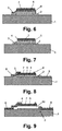
- a tuneable FBAR device 20 In a first embodiment, processing of a tuneable FBAR device 20 according to the present invention is described. Different methods, techniques and sequences may be used for processing a device 20 according to the invention. An example is described hereinafter. A possible sequence of process steps in the manufacture of the device 20 according to the invention is illustrated in Fig. 3-9. It has to be noted that this sequence is not limiting to the invention and that other sequences of process steps may be used to manufacture the device 20 of this invention.
- a substrate 1 is provided.
- the term “substrate” may include any underlying material or materials that may be used, or upon which a device, a circuit or an epitaxial layer may be formed.
- this "substrate” may include a semiconductor substrate such as e.g. a high-resistivity silicon, a doped silicon, a gallium arsenide (GaAs), a gallium arsenide phosphide (GaAsP), an indium phosphide (InP), a germanium (Ge), or a silicon germanium (SiGe) substrate.
- a semiconductor substrate such as e.g. a high-resistivity silicon, a doped silicon, a gallium arsenide (GaAs), a gallium arsenide phosphide (GaAsP), an indium phosphide (InP), a germanium (Ge), or a silicon germanium (SiGe) substrate.
- the "substrate” may include for example, an insulating layer such as a SiO 2 or an Si 3 N 4 layer in addition to a semiconductor substrate portion.
- the term substrate also includes silicon-on-glass, silicon-on sapphire substrates.
- substrate is thus used to define generally the elements for layers that underlie a layer or portions of interest.
- the "substrate” may be any other base on which a layer is formed, for example a glass or metal layer.
- a first conductive layer is deposited on top of the substrate 1.
- the first conductive layer may for example be a metal layer (e.g. copper, gold), an inorganic conductive layer (e.g. indium tin oxide (ITO)), a conductive polymer layer (polyaniline doped with camphor sulfonic acid (PANI/CSA)) or any other suitable conductive layer.
- the first conductive layer may be patterned by for example photolithography to form a firstelectrode 2, e.g. bottom electrode (see Fig. 3).
- the photolithography process comprises the following subsequent steps. First, a photoresist layer is applied on top of the first conductive layer on the substrate 1, e.g. by means of spincoating.
- the photoresist layer may for example have a thickness of a few ⁇ m and may be made of any suitable polymer that can be used as a photoresist, such as for example poly(vinyl cinnamate) or novolak-based polymers.
- a mask is applied to align a pattern onto the substrate 1.
- the photoresist layer is then illuminated through the mask e.g. by means of UV light.
- the photoresist is developed by which either the illuminated parts of the photoresist (positive resist) or the non-illuminated parts of the photoresist (negative resist) are removed, depending on which type of photoresist has been used. Patterning of the first conductive layer is then performed using the developed photoresist layer as a mask, after which the remaining parts of the photoresist layer are removed, typically by using an organic solvent.
- a sacrificial layer 3 is deposited on top of the substrate 1 and the first electrode 2, e.g. bottom electrode.
- the sacrificial layer 3 may be any suitable material that may be used as a sacrificial material such as for example a photoresist, SiO 2 or polyimide.
- the thickness of the sacrificial layer 3 will later determine the height of the airgap (see further) in the final device 20 and typically may be up to several ⁇ m and typically may be 500 nm..
- the sacrificial layer 3 may then be patterned by for example photolithography. The result after patterning is illustrated in Fig. 4.
- etch stop layer 4 a piezoelectric layer 5 and a second conductive layer 6 may be deposited (Fig. 5).
- the piezoelectric material of layer 5 may be any piezoelectric material permitted by processing technology, such as for example aluminium nitride (AIN). AIN may be grown on a seed layer such as for example Al or Pt, or any other suitable seed layer.
- the second conductive layer 6, which will after patterning result in a second electrode 7, e.g. top electrode 7, may be a metal layer (e.g. copper, gold), an inorganic conductive layer (e.g.
- ITO indium tin oxide
- PANI/CSA camphor sulfonic acid
- the second conductive layer 6, and hence the second electrode 7, top electrode 7, may either be formed of the same or of a different material as the material of the first electrode 2, e.g. bottom electrode.
- the piezoelectric layer 5 and the second conductive layer 6 may then be patterned by for example photolithography (Fig. 6).
- the etch stop layer 4 may prevent etching of the sacrificial layer 3 by the solvents used during patterning of the piezoelectric layer 5. However, if the solvents used during patterning of the piezoelectric layer 5 are such that they do not affect the sacrificial layer 3, no etch stop layer 4 is necessary. Thus, depending on the solvents used during patterning, deposition of an etch stop layer 4 may be optional.
- the etch stop layer 4 may be removed (see Fig. 7). This may be done by for example selective etching.
- the etch stop layer 4 may be formed out of copper, while the electrodes are for example made of Ta, ti or others. The etch stop layer 4 may then be removed by a selective etching solution that will only etch the copper layer and not the Ta or Ti layer.
- a third conductive layer may be deposited. Deposition of this layer may be done by any suitable technique such as for example chemical vapour deposition (CVD) or others.
- the third conductive layer preferably may be a metal layer such as for example copper or aluminium, but may also be any other suitable conductive layer.
- the third conductive layer may then be patterned as to form signal lines 8 (Fig. 8).
- a restraining bridge 9 may be formed (Fig. 8). This may be done by deposition and subsequent patterning of for example an Al layer. The restraining bridge 9 may be used for mechanical support and/or stability reasons of the structure of the device (20).
- the sacrificial layer 3 may be etched by means of for example selective etching.
- an oxygen plasma may be used to etch a photoresist sacrificial layer or a vapour HF etch may be used to etch a SiO 2 sacrificial layer.
- Etching of the sacrificial layer 3 is necessary to create an airgap 10 between the first electrode 2, e.g. bottom electrode 2 and the piezoelectric layer 5. In that way the FBAR structure is released.
- the height of the airgap 10 may be determined by the thickness of the sacrificial layer 3 and may for example be up to several ⁇ m, and typically may be 500 nm.
- the airgap 10 may be filled with a gas other than air or may be placed under vacuum.
- the layer will be referred to in the text and attached claims as a dielectric layer.
- top and bottom electrode instead of first and second electrode will be used for ease of understanding.
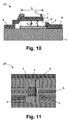
- the device 20 according to this first embodiment of the invention is shown in Fig. 10 (side view) and Fig. 11 (top view).
- a cantilever structure is formed by the piezoelectric layer 5, the top electrode 7, the optionally restraining bridge 9 and the signal line 8.
- actuation or tuning of the resonance frequency may be performed by changing a dimension of the device, in particular changing the height of the airgap 10 spacing t 1 .
- This also provides tuning by changing the relative position of components of the device.
- This may be done by a vertical movement of the cantilever structure, i.e. movement of the cantilever structure in a direction substantially perpendicular to the plane of the bottom electrode 2.
- This vertical movement may be achieved by different actuation mechanisms layer known to the skilled person and are for instance electrothermal, electromagnetic, electrodynamic, electrostatic, piezoelectric, shape memory and magneto-restrictive actuation.
- electrostatic movement of the piezoelectric cantilever is preferred. Actuators are described for instance in "The Mechatronics Handbook", CRC Press, 2002, for example chapter 20, especially section 20.5.
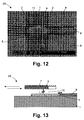
- Fig. 12 shows a SEM image of an FBAR device 20 according to this first embodiment of the present invention.
- the FBAR plate which comprises the piezoelectric layer 5 and the top electrode 7, holes 11 are formed which are intended to facilitate the release of the sacrificial layer 3.
- the material of the bottom electrode 2 may comprise a first metal and the top electrode 7 may comprise a second metal, the first and second metal being different from each other and being chosen such that there may be an automatic compensation for temperature dependency.
- Fig. 13 (side view) and Fig. 14 (top view) illustrate a tunable FBAR device 30 according to a second embodiment of the present invention.
- tuning of the resonance frequency is performed by changing the overlap area A, which is the overlap between the bottom electrode 2 and the piezoelectric layer 5, the overlap area A being defined by projection of the piezoelectric layer 5 onto the bottom electrode 2 according to a direction substantially perpendicular to the plane of the bottom electrode 2.
- This may be achieved by horizontal movement of the cantilever structure, i.e. movement of the cantilever structure in a direction substantially parallel to the plane of the bottom electrode 2.
- the device 30 of this invention may be comparable to the device 20 of the first embodiment, furthermore comprising a fixed comb 12 and a laterally movable comb 13, electrostatically interacting and generating a lateral movement of the piezoelectric layer 5, hereby reducing the overlap area A.
- the piezoelectric layer 5 is the layer which determines the area of the tuning capacitor.
- Different actuation mechanisms may be used in order to move elements of the FBAR. These are state of the art and are for instance electrothermal, electromagnetic, electrodynamic, electrostatic, piezoelectric, shape memory and magneto-restrictive actuation.
- Fig. 15 an equivalent electronic scheme is given for a device 20, 30 according to the present invention.
- the electrical equivalents of the acoustic (resonating) part of the FBAR are represented by L m , C m , R m .
- This part would determine the series resonant frequency of the circuit, if no tuning would be applied.
- C 0 represents the capacitance of the piezoelectric layer 5, R 0 the electrical loss in the piezoelectric layer 5,
- the cantilever structure with piezoelectric layer 5 moves in a vertical (first embodiment) or a horizontal (second embodiment) direction, i.e. in a direction substantially perpendicular resp. parallel to the plane of the bottom electrode 2.
- the design according to the present invention makes the tuning element an integrated part of the device 20, 30, thereby not only serving as the tuning element, but also as acoustic isolation and is expected to improve the overall quality factor by at least an order of magnitude.
- the Q factor is determined by the material properties and the parasitics.
- the Q factor of a resonant device may be defined by:
- a device is disclosed with a structure wherein the piezoelectric layer 5 is not in contact with any of the electrodes 2, 7. This is illustrated in Fig. 16.
- the device of this embodiment may be called a dual gap device, because as can be seen from Fig. 16, the piezoelectric layer 5 is not in contact with any of the electrodes 2, 7 and a gap 10, 14 is formed between the bottom electrode 2 and the piezoelectric layer 5 (thickness t 1 ) resp. between the top electrode 7 and the piezoelectric layer 5 (thickness t 2 ). Since there is no electrode 2, 7 in the acoustic path of the FBAR 40, it is possible to reach a very high Q factor. The value of the Q factor is mainly limited by the material loss of the piezoelectric layer 5, (Joel F. Rosenbaum "Bulk Acoustic Wave Theory and Devices", Artech House, 1988, ISBN 0-89006-265-X).
- the piezoelectric layer 5 may have an overlap A with the bottom electrode 2 and may have an overlap A' with the top electrode 7, the overlap A and A' being defined as the projection of the piezoelectric layer 5 onto the bottom electrode 2 resp. top electrode 7 in a direction substantially perpendicular to the plane of the bottom electrode 2 resp. top electrode 7.
- the frequency may be tuned by moving either one or both of the electrodes 2, 7 or the piezoelectric layer 5 itself in a vertical and/or horizontal direction, resp. defined as the direction substantially perpendicular and/or parallel to the plane of the bottom electrode 2.
- the overlap A and/or overlap A' and/or the thicknesses of the air gaps 10, 14, or more in general, the thicknesses t 1 , t 2 of the dielectric layers 10, 14, may be changed in order to achieve tuning.
- both airgaps 10, 14 may be varied.
- Moving the piezoelectric layer is an embodiment of the present invention in which a material with a dielectric constant greater than 1 is moved in or out of a part of the device where there is an electric field.
- the frequency tuning device or element is integrated into the FBAR instead of being implemented as a discrete external component.
- the tuning element may function as an acoustic isolation.
- the Q factor may preferably be higher than a few hundred and more preferably more higher than a few thousand. This is mainly due to the elimination of the contact between bottom electrode 2 and the piezoelectric layer 5 in a conventional sandwiched structure, the elimination of interconnections in the case of a discretely-coupled conventional approach, and the possibility of eliminating the piezoelectric layer 5-contacting electrodes in total.
- the airgap 10 tuning of the device 20, 30 may be performed by state-of-the art actuation methods as described before. Furthermore, the method according to the present invention is reversible. This means that tuning of the resonance frequency is not permanent. The resonance frequency may be tuned towards higher and lower frequencies.
- the present invention allows a lower power consumption compared with thermal tuning and offers real-time tunability. Furthermore, the device 20, 30 of the present invention allow a relative compensation of between 1 and 3%, whereas in the prior art only relative compensation of 0.1 % may be achieved.
- the embodiments according to the present invention may be produced with state-of-the-art surface micromachining techniques.
- Another tuning possibility of the first or third embodiment of the present invention may be post-pull-in tuning. This may be done when part of the movable structure is in its post-pull-in state and is touching the substrate. When the pull-in state is reached, it may still be possible to change the frequency if only part of the piezoelectric cantilever is touching the bottom electrode 2, but the change is really hard to precisely predicate.
- the device according to the first and third embodiment of the present invention may function as a switchable FBAR (from ante- to post-pull-in), i.e. the resonant frequency of the device may have a sharp transition before and after pull-in happens.
- a further embodiment of the present invention relates to an embodiment of the present invention in which a material with a dielectric constant greater than 1 is moved in or out of a part of the device where there is an electric field.
- This material is preferably a constituting element in the form of a solid piece or block of material which can controllably be moved. The material may be considered as part of device.
- a material is moved in or out of either or both of the spaces 10 or 14.
- This material has a dielectric constant greater than 1 and therefore influences the capacitance Cs 1 and/or Cs 2 to thereby tune the resonance frequency.
- Different actuation mechanisms may be used in order to move elements of the FBAR. These are state of the art and are for instance electrothermal, electromagnetic, electrodynamic, electrostatic, piezoelectric, shape memory and magneto-restrictive actuation.
- the FBAR device in accordance with any of the embodiments of the present invention can include means for automatically compensating for temperature changes, e.g. by using a bimetallic element which is associated with the means for altering an internal impedance.
- the piezoelectric layer and the top electrode can differ in thermal expansion coefficients. This may result in the top electrode moving closer to or further away from the bottom electrode as the temperature changes. This effect may be used to compensate for changes in the resonant frequency with temperature.
- the top electrode may be made of two differing metals which therefore act as a bi-metallic strip. Changes in temperature will cause the bi-metallic strip which forms the top electrode to move up or down with respect to the bottom electrode and careful choice of materials and thickness can be used to compensate for any changes in resonance frequency cause by changes in temperature.
- Fig. 17 show measured S 21 value with respect to signal frequencies for a device as described in the first embodiment of this invention.
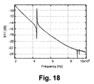
- Fig. 18 show measured S 11 value with respect to signal frequencies for the corresponding (Fig. 17 respectively) for the same specific embodiment according to the present invention.
- the S 11 parameter is a measure of the reflection coefficient of a component
- the S 21 parameter is a measure of the transmission coefficient of that component.
- S parameters are a representation of the properties of a network. The S21 and S11 parameters are often used to describe the transmission and reflection of a certain two-port network.
Landscapes
- Engineering & Computer Science (AREA)
- Power Engineering (AREA)
- Microelectronics & Electronic Packaging (AREA)
- Physics & Mathematics (AREA)
- Acoustics & Sound (AREA)
- Manufacturing & Machinery (AREA)
- Piezo-Electric Or Mechanical Vibrators, Or Delay Or Filter Circuits (AREA)
- Micromachines (AREA)
Priority Applications (1)
| Application Number | Priority Date | Filing Date | Title |
|---|---|---|---|
| EP04078526A EP1548768B1 (fr) | 2003-12-24 | 2004-12-24 | Résonateur à couche mince à micro-usinage |
Applications Claiming Priority (5)
| Application Number | Priority Date | Filing Date | Title |
|---|---|---|---|
| EP03447311 | 2003-12-24 | ||
| EP03447311A EP1548935A1 (fr) | 2003-12-24 | 2003-12-24 | Resonateur à couche mince à micro-usinage |
| US53332203P | 2003-12-29 | 2003-12-29 | |
| US533322P | 2003-12-29 | ||
| EP04078526A EP1548768B1 (fr) | 2003-12-24 | 2004-12-24 | Résonateur à couche mince à micro-usinage |
Publications (3)
| Publication Number | Publication Date |
|---|---|
| EP1548768A2 true EP1548768A2 (fr) | 2005-06-29 |
| EP1548768A3 EP1548768A3 (fr) | 2007-03-21 |
| EP1548768B1 EP1548768B1 (fr) | 2012-02-22 |
Family
ID=34556783
Family Applications (1)
| Application Number | Title | Priority Date | Filing Date |
|---|---|---|---|
| EP04078526A Expired - Lifetime EP1548768B1 (fr) | 2003-12-24 | 2004-12-24 | Résonateur à couche mince à micro-usinage |
Country Status (1)
| Country | Link |
|---|---|
| EP (1) | EP1548768B1 (fr) |
Cited By (4)
| Publication number | Priority date | Publication date | Assignee | Title |
|---|---|---|---|---|
| WO2012172166A1 (fr) * | 2011-06-15 | 2012-12-20 | Nokia Corporation | Électrode dotée d'un substrat d'actionnement à déformation réversible et procédés associés |
| WO2013134077A1 (fr) * | 2012-03-06 | 2013-09-12 | Qualcomm Mems Technologies, Inc. | Résonateur piézoélectrique à espace d'air |
| EP2507804A4 (fr) * | 2010-05-28 | 2015-06-17 | Lg Innotek Co Ltd | Condensateur variable et procédé pour le faire fonctionner |
| CN107528565A (zh) * | 2016-06-15 | 2017-12-29 | 三星电机株式会社 | 声波滤波器装置 |
Citations (5)
| Publication number | Priority date | Publication date | Assignee | Title |
|---|---|---|---|---|
| US5339051A (en) | 1991-12-09 | 1994-08-16 | Sandia Corporation | Micro-machined resonator oscillator |
| EP0631384A1 (fr) | 1993-06-10 | 1994-12-28 | Matsushita Electric Industrial Co., Ltd. | Dispositif piezoélectrique d'ondes acoustiques et procédé de fabrication |
| EP0963000A2 (fr) | 1998-06-02 | 1999-12-08 | Nokia Mobile Phones Ltd. | Structures de résonateurs |
| DE10153434A1 (de) | 2001-10-30 | 2003-05-15 | Epcos Ag | Megnetisch abstimmbares Filter |
| WO2003069776A2 (fr) | 2002-02-13 | 2003-08-21 | Commissariat A L'energie Atomique | Microresonateur mems a ondes acoustiques de volume accordable |
Family Cites Families (5)
| Publication number | Priority date | Publication date | Assignee | Title |
|---|---|---|---|---|
| US5747857A (en) * | 1991-03-13 | 1998-05-05 | Matsushita Electric Industrial Co., Ltd. | Electronic components having high-frequency elements and methods of manufacture therefor |
| US5491604A (en) * | 1992-12-11 | 1996-02-13 | The Regents Of The University Of California | Q-controlled microresonators and tunable electronic filters using such resonators |
| WO2001029853A1 (fr) * | 1999-10-16 | 2001-04-26 | Paralax, Llc | Condensateur variable sous vide |
| US6958566B2 (en) * | 2001-08-16 | 2005-10-25 | The Regents Of The University Of Michigan | Mechanical resonator device having phenomena-dependent electrical stiffness |
| US6741147B2 (en) * | 2002-09-30 | 2004-05-25 | Agere Systems Inc. | Method and apparatus for adjusting the resonant frequency of a thin film resonator |
-
2004
- 2004-12-24 EP EP04078526A patent/EP1548768B1/fr not_active Expired - Lifetime
Patent Citations (5)
| Publication number | Priority date | Publication date | Assignee | Title |
|---|---|---|---|---|
| US5339051A (en) | 1991-12-09 | 1994-08-16 | Sandia Corporation | Micro-machined resonator oscillator |
| EP0631384A1 (fr) | 1993-06-10 | 1994-12-28 | Matsushita Electric Industrial Co., Ltd. | Dispositif piezoélectrique d'ondes acoustiques et procédé de fabrication |
| EP0963000A2 (fr) | 1998-06-02 | 1999-12-08 | Nokia Mobile Phones Ltd. | Structures de résonateurs |
| DE10153434A1 (de) | 2001-10-30 | 2003-05-15 | Epcos Ag | Megnetisch abstimmbares Filter |
| WO2003069776A2 (fr) | 2002-02-13 | 2003-08-21 | Commissariat A L'energie Atomique | Microresonateur mems a ondes acoustiques de volume accordable |
Non-Patent Citations (1)
| Title |
|---|
| IEEE UFFC TRANSACTIONS, vol. 48, no. 5, September 2001 (2001-09-01), pages 189 - 1240 |
Cited By (6)
| Publication number | Priority date | Publication date | Assignee | Title |
|---|---|---|---|---|
| EP2507804A4 (fr) * | 2010-05-28 | 2015-06-17 | Lg Innotek Co Ltd | Condensateur variable et procédé pour le faire fonctionner |
| WO2012172166A1 (fr) * | 2011-06-15 | 2012-12-20 | Nokia Corporation | Électrode dotée d'un substrat d'actionnement à déformation réversible et procédés associés |
| US9324508B2 (en) | 2011-06-15 | 2016-04-26 | Nokia Technologies Oy | Substrate for electrode capable of undergoing reversible deformation |
| WO2013134077A1 (fr) * | 2012-03-06 | 2013-09-12 | Qualcomm Mems Technologies, Inc. | Résonateur piézoélectrique à espace d'air |
| CN107528565A (zh) * | 2016-06-15 | 2017-12-29 | 三星电机株式会社 | 声波滤波器装置 |
| CN107528565B (zh) * | 2016-06-15 | 2021-03-12 | 三星电机株式会社 | 声波滤波器装置 |
Also Published As
| Publication number | Publication date |
|---|---|
| EP1548768A3 (fr) | 2007-03-21 |
| EP1548768B1 (fr) | 2012-02-22 |
Similar Documents
| Publication | Publication Date | Title |
|---|---|---|
| US7372346B2 (en) | Acoustic resonator | |
| US10277188B2 (en) | Switchable filters and design structures | |
| US9935600B2 (en) | Switchable filters and design structures | |
| US9300272B2 (en) | Tunable filter structures and design structures | |
| US7023065B2 (en) | Capacitive resonators and methods of fabrication | |
| Jaafar et al. | A comprehensive study on RF MEMS switch | |
| JP4429918B2 (ja) | Mems圧電共振器 | |
| US10882736B2 (en) | Semiconductor structures provided within a cavity and related design structures | |
| EP1548935A1 (fr) | Resonateur à couche mince à micro-usinage | |
| US20020125030A1 (en) | High-Q micromechanical device and method of tuning same | |
| Shim et al. | A multimetal surface micromachining process for tunable RF MEMS passives | |
| EP1548768B1 (fr) | Résonateur à couche mince à micro-usinage | |
| US6846691B2 (en) | Method for making micromechanical structures having at least one lateral, small gap therebetween and micromechanical device produced thereby | |
| Zhao et al. | An Ultra-Low Impedance 4.8 GHz Al 72 Sc 28 N Resonant Rods Resonator With a Record k t 2 of 21.2% | |
| Jang et al. | RF MEMS suspended band-stop resonator and filter for frequency and bandwidth continuous fine tuning | |
| Rajagopalan | Reconfigurable RF communication components |
Legal Events
| Date | Code | Title | Description |
|---|---|---|---|
| PUAI | Public reference made under article 153(3) epc to a published international application that has entered the european phase |
Free format text: ORIGINAL CODE: 0009012 |
|
| AK | Designated contracting states |
Kind code of ref document: A2 Designated state(s): AT BE BG CH CY CZ DE DK EE ES FI FR GB GR HU IE IS IT LI LT LU MC NL PL PT RO SE SI SK TR |
|
| AX | Request for extension of the european patent |
Extension state: AL BA HR LV MK YU |
|
| PUAL | Search report despatched |
Free format text: ORIGINAL CODE: 0009013 |
|
| AK | Designated contracting states |
Kind code of ref document: A3 Designated state(s): AT BE BG CH CY CZ DE DK EE ES FI FR GB GR HU IE IS IT LI LT LU MC NL PL PT RO SE SI SK TR |
|
| AX | Request for extension of the european patent |
Extension state: AL BA HR LV MK YU |
|
| 17P | Request for examination filed |
Effective date: 20070921 |
|
| AKX | Designation fees paid |
Designated state(s): AT BE BG CH CY CZ DE DK EE ES FI FR GB GR HU IE IS IT LI LT LU MC NL PL PT RO SE SI SK TR |
|
| RAP1 | Party data changed (applicant data changed or rights of an application transferred) |
Owner name: IMEC |
|
| 17Q | First examination report despatched |
Effective date: 20101021 |
|
| REG | Reference to a national code |
Ref country code: DE Ref legal event code: R079 Ref document number: 602004036564 Country of ref document: DE Free format text: PREVIOUS MAIN CLASS: H01G0005140000 Ipc: H03H0003040000 |
|
| RIC1 | Information provided on ipc code assigned before grant |
Ipc: H03H 3/04 20060101AFI20110728BHEP Ipc: H03H 3/02 20060101ALI20110728BHEP Ipc: H01G 5/14 20060101ALI20110728BHEP Ipc: H03H 9/02 20060101ALI20110728BHEP Ipc: H03H 9/17 20060101ALI20110728BHEP |
|
| GRAP | Despatch of communication of intention to grant a patent |
Free format text: ORIGINAL CODE: EPIDOSNIGR1 |
|
| GRAS | Grant fee paid |
Free format text: ORIGINAL CODE: EPIDOSNIGR3 |
|
| GRAA | (expected) grant |
Free format text: ORIGINAL CODE: 0009210 |
|
| AK | Designated contracting states |
Kind code of ref document: B1 Designated state(s): AT BE BG CH CY CZ DE DK EE ES FI FR GB GR HU IE IS IT LI LT LU MC NL PL PT RO SE SI SK TR |
|
| REG | Reference to a national code |
Ref country code: GB Ref legal event code: FG4D |
|
| REG | Reference to a national code |
Ref country code: CH Ref legal event code: EP |
|
| REG | Reference to a national code |
Ref country code: AT Ref legal event code: REF Ref document number: 546881 Country of ref document: AT Kind code of ref document: T Effective date: 20120315 |
|
| REG | Reference to a national code |
Ref country code: IE Ref legal event code: FG4D |
|
| REG | Reference to a national code |
Ref country code: DE Ref legal event code: R096 Ref document number: 602004036564 Country of ref document: DE Effective date: 20120419 |
|
| REG | Reference to a national code |
Ref country code: NL Ref legal event code: VDEP Effective date: 20120222 |
|
| LTIE | Lt: invalidation of european patent or patent extension |
Effective date: 20120222 |
|
| PG25 | Lapsed in a contracting state [announced via postgrant information from national office to epo] |
Ref country code: IS Free format text: LAPSE BECAUSE OF FAILURE TO SUBMIT A TRANSLATION OF THE DESCRIPTION OR TO PAY THE FEE WITHIN THE PRESCRIBED TIME-LIMIT Effective date: 20120622 Ref country code: NL Free format text: LAPSE BECAUSE OF FAILURE TO SUBMIT A TRANSLATION OF THE DESCRIPTION OR TO PAY THE FEE WITHIN THE PRESCRIBED TIME-LIMIT Effective date: 20120222 Ref country code: LT Free format text: LAPSE BECAUSE OF FAILURE TO SUBMIT A TRANSLATION OF THE DESCRIPTION OR TO PAY THE FEE WITHIN THE PRESCRIBED TIME-LIMIT Effective date: 20120222 |
|
| PG25 | Lapsed in a contracting state [announced via postgrant information from national office to epo] |
Ref country code: PT Free format text: LAPSE BECAUSE OF FAILURE TO SUBMIT A TRANSLATION OF THE DESCRIPTION OR TO PAY THE FEE WITHIN THE PRESCRIBED TIME-LIMIT Effective date: 20120622 Ref country code: BE Free format text: LAPSE BECAUSE OF FAILURE TO SUBMIT A TRANSLATION OF THE DESCRIPTION OR TO PAY THE FEE WITHIN THE PRESCRIBED TIME-LIMIT Effective date: 20120222 Ref country code: FI Free format text: LAPSE BECAUSE OF FAILURE TO SUBMIT A TRANSLATION OF THE DESCRIPTION OR TO PAY THE FEE WITHIN THE PRESCRIBED TIME-LIMIT Effective date: 20120222 Ref country code: GR Free format text: LAPSE BECAUSE OF FAILURE TO SUBMIT A TRANSLATION OF THE DESCRIPTION OR TO PAY THE FEE WITHIN THE PRESCRIBED TIME-LIMIT Effective date: 20120523 |
|
| REG | Reference to a national code |
Ref country code: AT Ref legal event code: MK05 Ref document number: 546881 Country of ref document: AT Kind code of ref document: T Effective date: 20120222 |
|
| PG25 | Lapsed in a contracting state [announced via postgrant information from national office to epo] |
Ref country code: CY Free format text: LAPSE BECAUSE OF FAILURE TO SUBMIT A TRANSLATION OF THE DESCRIPTION OR TO PAY THE FEE WITHIN THE PRESCRIBED TIME-LIMIT Effective date: 20120222 |
|
| PG25 | Lapsed in a contracting state [announced via postgrant information from national office to epo] |
Ref country code: SI Free format text: LAPSE BECAUSE OF FAILURE TO SUBMIT A TRANSLATION OF THE DESCRIPTION OR TO PAY THE FEE WITHIN THE PRESCRIBED TIME-LIMIT Effective date: 20120222 Ref country code: DK Free format text: LAPSE BECAUSE OF FAILURE TO SUBMIT A TRANSLATION OF THE DESCRIPTION OR TO PAY THE FEE WITHIN THE PRESCRIBED TIME-LIMIT Effective date: 20120222 Ref country code: EE Free format text: LAPSE BECAUSE OF FAILURE TO SUBMIT A TRANSLATION OF THE DESCRIPTION OR TO PAY THE FEE WITHIN THE PRESCRIBED TIME-LIMIT Effective date: 20120222 Ref country code: RO Free format text: LAPSE BECAUSE OF FAILURE TO SUBMIT A TRANSLATION OF THE DESCRIPTION OR TO PAY THE FEE WITHIN THE PRESCRIBED TIME-LIMIT Effective date: 20120222 Ref country code: SE Free format text: LAPSE BECAUSE OF FAILURE TO SUBMIT A TRANSLATION OF THE DESCRIPTION OR TO PAY THE FEE WITHIN THE PRESCRIBED TIME-LIMIT Effective date: 20120222 Ref country code: CZ Free format text: LAPSE BECAUSE OF FAILURE TO SUBMIT A TRANSLATION OF THE DESCRIPTION OR TO PAY THE FEE WITHIN THE PRESCRIBED TIME-LIMIT Effective date: 20120222 Ref country code: PL Free format text: LAPSE BECAUSE OF FAILURE TO SUBMIT A TRANSLATION OF THE DESCRIPTION OR TO PAY THE FEE WITHIN THE PRESCRIBED TIME-LIMIT Effective date: 20120222 |
|
| PG25 | Lapsed in a contracting state [announced via postgrant information from national office to epo] |
Ref country code: SK Free format text: LAPSE BECAUSE OF FAILURE TO SUBMIT A TRANSLATION OF THE DESCRIPTION OR TO PAY THE FEE WITHIN THE PRESCRIBED TIME-LIMIT Effective date: 20120222 Ref country code: IT Free format text: LAPSE BECAUSE OF FAILURE TO SUBMIT A TRANSLATION OF THE DESCRIPTION OR TO PAY THE FEE WITHIN THE PRESCRIBED TIME-LIMIT Effective date: 20120222 |
|
| PLBE | No opposition filed within time limit |
Free format text: ORIGINAL CODE: 0009261 |
|
| STAA | Information on the status of an ep patent application or granted ep patent |
Free format text: STATUS: NO OPPOSITION FILED WITHIN TIME LIMIT |
|
| 26N | No opposition filed |
Effective date: 20121123 |
|
| PG25 | Lapsed in a contracting state [announced via postgrant information from national office to epo] |
Ref country code: AT Free format text: LAPSE BECAUSE OF FAILURE TO SUBMIT A TRANSLATION OF THE DESCRIPTION OR TO PAY THE FEE WITHIN THE PRESCRIBED TIME-LIMIT Effective date: 20120222 |
|
| REG | Reference to a national code |
Ref country code: DE Ref legal event code: R097 Ref document number: 602004036564 Country of ref document: DE Effective date: 20121123 |
|
| PG25 | Lapsed in a contracting state [announced via postgrant information from national office to epo] |
Ref country code: ES Free format text: LAPSE BECAUSE OF FAILURE TO SUBMIT A TRANSLATION OF THE DESCRIPTION OR TO PAY THE FEE WITHIN THE PRESCRIBED TIME-LIMIT Effective date: 20120602 |
|
| PG25 | Lapsed in a contracting state [announced via postgrant information from national office to epo] |
Ref country code: MC Free format text: LAPSE BECAUSE OF NON-PAYMENT OF DUE FEES Effective date: 20121231 Ref country code: BG Free format text: LAPSE BECAUSE OF FAILURE TO SUBMIT A TRANSLATION OF THE DESCRIPTION OR TO PAY THE FEE WITHIN THE PRESCRIBED TIME-LIMIT Effective date: 20120522 |
|
| REG | Reference to a national code |
Ref country code: CH Ref legal event code: PL |
|
| REG | Reference to a national code |
Ref country code: IE Ref legal event code: MM4A |
|
| PG25 | Lapsed in a contracting state [announced via postgrant information from national office to epo] |
Ref country code: IE Free format text: LAPSE BECAUSE OF NON-PAYMENT OF DUE FEES Effective date: 20121224 Ref country code: CH Free format text: LAPSE BECAUSE OF NON-PAYMENT OF DUE FEES Effective date: 20121231 Ref country code: LI Free format text: LAPSE BECAUSE OF NON-PAYMENT OF DUE FEES Effective date: 20121231 |
|
| PG25 | Lapsed in a contracting state [announced via postgrant information from national office to epo] |
Ref country code: TR Free format text: LAPSE BECAUSE OF FAILURE TO SUBMIT A TRANSLATION OF THE DESCRIPTION OR TO PAY THE FEE WITHIN THE PRESCRIBED TIME-LIMIT Effective date: 20120222 |
|
| PG25 | Lapsed in a contracting state [announced via postgrant information from national office to epo] |
Ref country code: LU Free format text: LAPSE BECAUSE OF NON-PAYMENT OF DUE FEES Effective date: 20121224 |
|
| PG25 | Lapsed in a contracting state [announced via postgrant information from national office to epo] |
Ref country code: HU Free format text: LAPSE BECAUSE OF FAILURE TO SUBMIT A TRANSLATION OF THE DESCRIPTION OR TO PAY THE FEE WITHIN THE PRESCRIBED TIME-LIMIT Effective date: 20041224 |
|
| REG | Reference to a national code |
Ref country code: FR Ref legal event code: PLFP Year of fee payment: 12 |
|
| REG | Reference to a national code |
Ref country code: FR Ref legal event code: PLFP Year of fee payment: 13 |
|
| REG | Reference to a national code |
Ref country code: FR Ref legal event code: PLFP Year of fee payment: 14 |
|
| PGFP | Annual fee paid to national office [announced via postgrant information from national office to epo] |
Ref country code: DE Payment date: 20191119 Year of fee payment: 16 |
|
| PGFP | Annual fee paid to national office [announced via postgrant information from national office to epo] |
Ref country code: FR Payment date: 20191120 Year of fee payment: 16 |
|
| PGFP | Annual fee paid to national office [announced via postgrant information from national office to epo] |
Ref country code: GB Payment date: 20191122 Year of fee payment: 16 |
|
| REG | Reference to a national code |
Ref country code: DE Ref legal event code: R119 Ref document number: 602004036564 Country of ref document: DE |
|
| GBPC | Gb: european patent ceased through non-payment of renewal fee |
Effective date: 20201224 |
|
| PG25 | Lapsed in a contracting state [announced via postgrant information from national office to epo] |
Ref country code: FR Free format text: LAPSE BECAUSE OF NON-PAYMENT OF DUE FEES Effective date: 20201231 |
|
| PG25 | Lapsed in a contracting state [announced via postgrant information from national office to epo] |
Ref country code: GB Free format text: LAPSE BECAUSE OF NON-PAYMENT OF DUE FEES Effective date: 20201224 Ref country code: DE Free format text: LAPSE BECAUSE OF NON-PAYMENT OF DUE FEES Effective date: 20210701 |