EP1548809B1 - WûRMEBEHANDLUNGSVERFAHREN UND WûRMEBEHANDLUNGSVORRICHTUNG - Google Patents
WûRMEBEHANDLUNGSVERFAHREN UND WûRMEBEHANDLUNGSVORRICHTUNG Download PDFInfo
- Publication number
- EP1548809B1 EP1548809B1 EP03784632A EP03784632A EP1548809B1 EP 1548809 B1 EP1548809 B1 EP 1548809B1 EP 03784632 A EP03784632 A EP 03784632A EP 03784632 A EP03784632 A EP 03784632A EP 1548809 B1 EP1548809 B1 EP 1548809B1
- Authority
- EP
- European Patent Office
- Prior art keywords
- substrates
- thermal processing
- wafers
- thermal
- production
- Prior art date
- Legal status (The legal status is an assumption and is not a legal conclusion. Google has not performed a legal analysis and makes no representation as to the accuracy of the status listed.)
- Expired - Lifetime
Links
Images


Classifications
-
- H—ELECTRICITY
- H10—SEMICONDUCTOR DEVICES; ELECTRIC SOLID-STATE DEVICES NOT OTHERWISE PROVIDED FOR
- H10P—GENERIC PROCESSES OR APPARATUS FOR THE MANUFACTURE OR TREATMENT OF DEVICES COVERED BY CLASS H10
- H10P72/00—Handling or holding of wafers, substrates or devices during manufacture or treatment thereof
- H10P72/06—Apparatus for monitoring, sorting, marking, testing or measuring
- H10P72/0604—Process monitoring, e.g. flow or thickness monitoring
-
- C—CHEMISTRY; METALLURGY
- C23—COATING METALLIC MATERIAL; COATING MATERIAL WITH METALLIC MATERIAL; CHEMICAL SURFACE TREATMENT; DIFFUSION TREATMENT OF METALLIC MATERIAL; COATING BY VACUUM EVAPORATION, BY SPUTTERING, BY ION IMPLANTATION OR BY CHEMICAL VAPOUR DEPOSITION, IN GENERAL; INHIBITING CORROSION OF METALLIC MATERIAL OR INCRUSTATION IN GENERAL
- C23C—COATING METALLIC MATERIAL; COATING MATERIAL WITH METALLIC MATERIAL; SURFACE TREATMENT OF METALLIC MATERIAL BY DIFFUSION INTO THE SURFACE, BY CHEMICAL CONVERSION OR SUBSTITUTION; COATING BY VACUUM EVAPORATION, BY SPUTTERING, BY ION IMPLANTATION OR BY CHEMICAL VAPOUR DEPOSITION, IN GENERAL
- C23C16/00—Chemical coating by decomposition of gaseous compounds, without leaving reaction products of surface material in the coating, i.e. chemical vapour deposition [CVD] processes
- C23C16/44—Chemical coating by decomposition of gaseous compounds, without leaving reaction products of surface material in the coating, i.e. chemical vapour deposition [CVD] processes characterised by the method of coating
- C23C16/46—Chemical coating by decomposition of gaseous compounds, without leaving reaction products of surface material in the coating, i.e. chemical vapour deposition [CVD] processes characterised by the method of coating characterised by the method used for heating the substrate
-
- C—CHEMISTRY; METALLURGY
- C23—COATING METALLIC MATERIAL; COATING MATERIAL WITH METALLIC MATERIAL; CHEMICAL SURFACE TREATMENT; DIFFUSION TREATMENT OF METALLIC MATERIAL; COATING BY VACUUM EVAPORATION, BY SPUTTERING, BY ION IMPLANTATION OR BY CHEMICAL VAPOUR DEPOSITION, IN GENERAL; INHIBITING CORROSION OF METALLIC MATERIAL OR INCRUSTATION IN GENERAL
- C23C—COATING METALLIC MATERIAL; COATING MATERIAL WITH METALLIC MATERIAL; SURFACE TREATMENT OF METALLIC MATERIAL BY DIFFUSION INTO THE SURFACE, BY CHEMICAL CONVERSION OR SUBSTITUTION; COATING BY VACUUM EVAPORATION, BY SPUTTERING, BY ION IMPLANTATION OR BY CHEMICAL VAPOUR DEPOSITION, IN GENERAL
- C23C16/00—Chemical coating by decomposition of gaseous compounds, without leaving reaction products of surface material in the coating, i.e. chemical vapour deposition [CVD] processes
- C23C16/44—Chemical coating by decomposition of gaseous compounds, without leaving reaction products of surface material in the coating, i.e. chemical vapour deposition [CVD] processes characterised by the method of coating
- C23C16/52—Controlling or regulating the coating process
-
- H—ELECTRICITY
- H10—SEMICONDUCTOR DEVICES; ELECTRIC SOLID-STATE DEVICES NOT OTHERWISE PROVIDED FOR
- H10P—GENERIC PROCESSES OR APPARATUS FOR THE MANUFACTURE OR TREATMENT OF DEVICES COVERED BY CLASS H10
- H10P14/00—Formation of materials, e.g. in the shape of layers or pillars
- H10P14/60—Formation of materials, e.g. in the shape of layers or pillars of insulating materials
- H10P14/63—Formation of materials, e.g. in the shape of layers or pillars of insulating materials characterised by the formation processes
- H10P14/6302—Non-deposition formation processes
- H10P14/6304—Formation by oxidation, e.g. oxidation of the substrate
- H10P14/6306—Formation by oxidation, e.g. oxidation of the substrate of the semiconductor materials
- H10P14/6308—Formation by oxidation, e.g. oxidation of the substrate of the semiconductor materials of Group IV semiconductors
- H10P14/6309—Formation by oxidation, e.g. oxidation of the substrate of the semiconductor materials of Group IV semiconductors of silicon in uncombined form, i.e. pure silicon
-
- H—ELECTRICITY
- H10—SEMICONDUCTOR DEVICES; ELECTRIC SOLID-STATE DEVICES NOT OTHERWISE PROVIDED FOR
- H10P—GENERIC PROCESSES OR APPARATUS FOR THE MANUFACTURE OR TREATMENT OF DEVICES COVERED BY CLASS H10
- H10P14/00—Formation of materials, e.g. in the shape of layers or pillars
- H10P14/60—Formation of materials, e.g. in the shape of layers or pillars of insulating materials
- H10P14/63—Formation of materials, e.g. in the shape of layers or pillars of insulating materials characterised by the formation processes
- H10P14/6302—Non-deposition formation processes
- H10P14/6322—Formation by thermal treatments
-
- H—ELECTRICITY
- H10—SEMICONDUCTOR DEVICES; ELECTRIC SOLID-STATE DEVICES NOT OTHERWISE PROVIDED FOR
- H10P—GENERIC PROCESSES OR APPARATUS FOR THE MANUFACTURE OR TREATMENT OF DEVICES COVERED BY CLASS H10
- H10P14/00—Formation of materials, e.g. in the shape of layers or pillars
- H10P14/60—Formation of materials, e.g. in the shape of layers or pillars of insulating materials
- H10P14/63—Formation of materials, e.g. in the shape of layers or pillars of insulating materials characterised by the formation processes
- H10P14/6326—Deposition processes
- H10P14/6328—Deposition from the gas or vapour phase
- H10P14/6334—Deposition from the gas or vapour phase using decomposition or reaction of gaseous or vapour phase compounds, i.e. chemical vapour deposition
-
- H—ELECTRICITY
- H10—SEMICONDUCTOR DEVICES; ELECTRIC SOLID-STATE DEVICES NOT OTHERWISE PROVIDED FOR
- H10P—GENERIC PROCESSES OR APPARATUS FOR THE MANUFACTURE OR TREATMENT OF DEVICES COVERED BY CLASS H10
- H10P14/00—Formation of materials, e.g. in the shape of layers or pillars
- H10P14/60—Formation of materials, e.g. in the shape of layers or pillars of insulating materials
- H10P14/66—Formation of materials, e.g. in the shape of layers or pillars of insulating materials characterised by the type of materials
- H10P14/668—Formation of materials, e.g. in the shape of layers or pillars of insulating materials characterised by the type of materials the materials being characterised by the deposition precursor materials
- H10P14/6681—Formation of materials, e.g. in the shape of layers or pillars of insulating materials characterised by the type of materials the materials being characterised by the deposition precursor materials the precursor containing a compound comprising Si
- H10P14/6682—Formation of materials, e.g. in the shape of layers or pillars of insulating materials characterised by the type of materials the materials being characterised by the deposition precursor materials the precursor containing a compound comprising Si the compound being a silane, e.g. disilane, methylsilane or chlorosilane
-
- H—ELECTRICITY
- H10—SEMICONDUCTOR DEVICES; ELECTRIC SOLID-STATE DEVICES NOT OTHERWISE PROVIDED FOR
- H10P—GENERIC PROCESSES OR APPARATUS FOR THE MANUFACTURE OR TREATMENT OF DEVICES COVERED BY CLASS H10
- H10P14/00—Formation of materials, e.g. in the shape of layers or pillars
- H10P14/60—Formation of materials, e.g. in the shape of layers or pillars of insulating materials
- H10P14/69—Inorganic materials
- H10P14/694—Inorganic materials composed of nitrides
- H10P14/6943—Inorganic materials composed of nitrides containing silicon
- H10P14/69433—Inorganic materials composed of nitrides containing silicon the material being a silicon nitride not containing oxygen, e.g. SixNy or SixByNz
-
- H—ELECTRICITY
- H10—SEMICONDUCTOR DEVICES; ELECTRIC SOLID-STATE DEVICES NOT OTHERWISE PROVIDED FOR
- H10P—GENERIC PROCESSES OR APPARATUS FOR THE MANUFACTURE OR TREATMENT OF DEVICES COVERED BY CLASS H10
- H10P72/00—Handling or holding of wafers, substrates or devices during manufacture or treatment thereof
- H10P72/04—Apparatus for manufacture or treatment
- H10P72/0431—Apparatus for thermal treatment
- H10P72/0434—Apparatus for thermal treatment mainly by convection
-
- H—ELECTRICITY
- H10—SEMICONDUCTOR DEVICES; ELECTRIC SOLID-STATE DEVICES NOT OTHERWISE PROVIDED FOR
- H10P—GENERIC PROCESSES OR APPARATUS FOR THE MANUFACTURE OR TREATMENT OF DEVICES COVERED BY CLASS H10
- H10P72/00—Handling or holding of wafers, substrates or devices during manufacture or treatment thereof
- H10P72/06—Apparatus for monitoring, sorting, marking, testing or measuring
- H10P72/0602—Temperature monitoring
-
- H—ELECTRICITY
- H10—SEMICONDUCTOR DEVICES; ELECTRIC SOLID-STATE DEVICES NOT OTHERWISE PROVIDED FOR
- H10P—GENERIC PROCESSES OR APPARATUS FOR THE MANUFACTURE OR TREATMENT OF DEVICES COVERED BY CLASS H10
- H10P74/00—Testing or measuring during manufacture or treatment of wafers, substrates or devices
- H10P74/23—Testing or measuring during manufacture or treatment of wafers, substrates or devices characterised by multiple measurements, corrections, marking or sorting processes
-
- Y—GENERAL TAGGING OF NEW TECHNOLOGICAL DEVELOPMENTS; GENERAL TAGGING OF CROSS-SECTIONAL TECHNOLOGIES SPANNING OVER SEVERAL SECTIONS OF THE IPC; TECHNICAL SUBJECTS COVERED BY FORMER USPC CROSS-REFERENCE ART COLLECTIONS [XRACs] AND DIGESTS
- Y10—TECHNICAL SUBJECTS COVERED BY FORMER USPC
- Y10T—TECHNICAL SUBJECTS COVERED BY FORMER US CLASSIFICATION
- Y10T436/00—Chemistry: analytical and immunological testing
- Y10T436/25—Chemistry: analytical and immunological testing including sample preparation
Definitions
- the present invention relates to a thermal processing method and a thermal processing unit of a batch type, wherein a thermal process is conducted to a large number of substrates such as semiconductor wafers at a time.
- thermal processing unit of a batch type that carries out such a thermal process a longitudinal type of thermal processing unit is known.
- a holder which is called a wafer boat
- the holder is conveyed into a longitudinal type of thermal processing furnace, for example thorough a lower part of the thermal processing furnace.
- atmosphere in the thermal processing furnace is made to be heating atmosphere of a predetermined temperature, and a thermal process is conducted.
- area of the thermal processing furnace to be heated is vertically divided into a plurality of zones, and a heating unit and a temperature controller are provided for each zone in order to enable a temperature control for each zone.
- Fig. 10 is a longitudinal sectional view of an oxidation processing unit as an example of a longitudinal thermal processing unit.
- 11 represents a reaction container whose lower end is open.
- Gas-supplying pipes 12 and 13 for supplying a or more gases for the oxidation process, such as an oxygen gas and a hydrogen-chloride gas, into the reaction container 11, and a gas-discharging pipe 15 that extends to a gas-discharging pump 14, are connected to a lower end portion of the reaction container 11.
- the gas-supplying pipes 12 and 13 are bent upward in the reaction container 11, and are opened in the vicinity of a ceiling part of the reaction container 11 to supply the respective gases therefrom.
- 16 represents a plurality of vertically-divided heaters provided around the reaction container 11.
- 17 represents a wafer boat for holding a large number of wafers W in a tier-like manner.
- a flow of an oxidation process using the apparatus shown in Fig. 10 is briefly explained as follows. At first, for example 140 wafers W having surfaces on which silicon layers have been formed are conveyed onto the wafer boat 17. Then, the wafer boat 17 is conveyed into the reaction container 11. At that time, a lower-end opening 19 of the reaction container 11 is hermetically sealed by a lid 18 provided at a lower end of the wafer boat 17. Then, the inside of the reaction container 11 is heated to a predetermined temperature, and maintained in a state of a slightly-reduced pressure. Under the state, the process gas or gases, such as an oxygen gas and a hydrogen-chloride gas, are introduced into the reaction container 11, and thus surfaces of the wafers W are oxidized to form silicon oxide films.
- the process gas or gases such as an oxygen gas and a hydrogen-chloride gas
- temperature set values for example, dummy wafers having surfaces on which silicon oxide films have been formed are held by the wafer boat 17 in accordance with a layout depending on an arrangement layout of production wafers to be processed. Then, the thermal process (oxidation process) is conducted in accordance with predetermined temperature set values in such a manner that thickness of obtained (formed) oxide films substantially coincides with a target thickness. Then, thickness of the silicon oxide films is measured for each zone of the thermal processing atmosphere, a calculation is conducted based on a relationship between variation of the film thickness and variation of the temperature set values of the respective heaters 16, which has been obtained in advance, and then the temperature set values are corrected.
- the above correction is repeatedly conducted until the thickness profile is maintained within an error range of the target thickness.
- the inventor has studied a method of: creating reduced-pressure atmosphere in a reaction container, generating active species including O-radical and OH-radical by introducing a hydrogen gas and an oxygen gas into the reaction container at predetermined flow rates and by heating them to for example about 1000 °C, and forming oxide films onto wafers by means of the radicals.
- oxide films having good film quality can be obtained because an oxidative effect of the method is stronger than those of dry oxidation process and wet oxidation process.
- the above document reveals that production wafers are used for the above adjusting operation.
- the temperature adjusting operation includes a plurality of thermal processes.
- burden of cost is great, which is not preferable. Therefore, in general, dummy wafers are used for the temperature adjusting operation.
- Fig. 11 shows a result of an experiment for confirming the loading effect.
- the temperature set values of the respective heaters 16 for the respective zones were adjusted to values according to which uniformity of film thickness between surfaces is expected to be satisfactory.
- wafers W are fully arranged onto the wafer boat 17.
- An oxidation process by radicals was conducted under the same condition for the following three cases: a case wherein all the wafers W were dummy wafers; a case wherein 22 wafers (trench wafers) whose surfaces have trench structures were arranged, and a case wherein 39 trench wafers were arranged.
- Film thickness profile was measured for each case.
- ⁇ is the result for the case wherein all the wafers W were dummy wafers.
- A is the result for the case wherein 22 trench wafers were used.
- ⁇ is the result for the case wherein 39 trench wafers were used.
- the flow rate of the process gas is increased, uniformity of film thickness within a surface of each substrate may be decreased.
- the pressure of the reaction chamber 11 is increased, and hence the radicals may easily lose activity, that is, lifetime of the radicals may be shortened.
- the oxidation process using the radicals may suffer from the loading effect in the conventional manner, so that it is difficult to secure high uniformity of film quality of the oxide films between surfaces.
- process condition such as a temperature is determined depending on the arrangement layout of the production wafers
- the setting operation of the process condition is troublesome.
- process condition such as a temperature of each zone of the reaction container, a pressure, a gas flow rate and a processing time, is set depending on the number and/or the arrangement layout of production wafers arranged on the wafer boat, some operation miss is likely to occur.
- US 6,211,094 B1 describes a method of controlling thickness of thin film layers manufactured in a semiconductor manufacturing apparatus.
- the apparatus has multiple film formation zones wherein one of the zones is a reference zone.
- thicknesses of the thin films are measured.
- process time and process temperatures are adjusted so that equal thicknesses are achieved.
- thin films are formed on semiconductor wafers using the adjusted process time and temperatures.
- the object of this invention is to provide a technique that can improve uniformity of film thickness of thin films between surfaces when the thin films are formed on the surfaces of respective substrates by conducting a thermal process to a plurality of substrates at one time.
- another object of this invention is to provide a technique that can obtain the same process result independent on the number of productions to be thermally processed, with less operator's burden.
- the present invention provides a thermal processing method according to claim 1.
- the plurality of zones of thermal process atmosphere in the reaction container may not be physically divided. Boundaries between the plurality of zones may not be clear. If is sufficient for the heating units to be respectively provided for the corresponding zones.
- the thickness of the thin films on the first substrates or the second substrates may be measured directly.
- some of the first substrates or the second substrates may be replaced with monitor substrates to be measured, and then, after the thermal process, thickness of thin films formed on the monitor substrates may be measured as the thickness of the thin films on the first substrates or the second substrates.
- the monitor substrates are arranged at regular intervals.
- the temperature set values for the thermal process are set by using the first substrates and then corrected by using the second substrates, wherein the first substrates need less consumption of the process gas than the production substrates and the second substrates need more consumption of the process gas than the first substrates, even if there is some loading effect (phenomenon in which thickness of thin films formed on substrates located on a downstream side of the process gas is thinner, because substrates located on an upstream side thereof consume the process gas), the difference with the target thickness that may be caused by the loading effect may be canceled by the correction of the temperature set values.
- high uniformity of film thickness of the thin films on production substrates may be obtained between the zones.
- the first setting step and the second correcting step may be respectively carried out based on a relationship between variation of the temperature set values and variation of the thickness of the thin films, which has been obtained in advance.
- the process gas may be activated to generate active species, and oxide films may be formed on the surfaces of the substrates by means of the active species.
- the process gas comprises a hydrogen gas and an oxygen gas.
- the first substrates are substrates on which oxide films having an average thickness of 50 nm or more have been formed in advance.
- the second substrates are bare silicon substrates.
- the thin films are formed on the surfaces of the substrates by means of a chemical vapor deposition.
- the first substrates are substrates having surfaces on which patterns have not been formed
- the second substrates are substrates having surfaces on which patterns have been formed.
- the first substrates in the first thermal processing step, may be fully arranged in a holding region for substrates to be processed in the substrate holder, and in the second thermal processing step, the second substrates may be fully arranged in the holding region for substrates to be processed in the substrate holder.
- production substrates may be fully arranged in the holding region for substrates to be processed in the substrate holder.
- less number of production substrates may be arranged.
- the production substrates are arranged at a portion on an upstream side of a flow of the process gas introduced into the reaction container, in the holding region for substrates to be processed in the substrate holder, and the first substrates are arranged at the residual portion in the holding region.
- the same thermal processing result can be obtained.
- operator's burden may be reduced and miss in setting temperatures may be prevented.
- a pressure in the reaction container, a flow rate of the process gas and a time of the thermal process may be common in the second thermal processing step and in the third thermal processing step.
- the present invention also provides a control unit for a thermal processing unit according to claim 12 and a thermal processing unit according to claim 13.
- the first substrates when the thermal process is carried out to the plurality of first substrates, the first substrates may be fully arranged in a holding region for substrates to be processed in the substrate holder, and when the thermal process is carried out to the plurality of second substrates, the second substrates may be fully arranged in the holding region for substrates to be processed in the substrate holder.
- the thermal processing unit further comprises a substrate-conveying unit that conveys a substrate onto the substrate holder, wherein the production-substrate thermal processing part is adapted to control the substrate-conveying unit in such a manner that when the thermal process is carried out to at least the plurality of the production substrates, the production substrates are arranged at a portion on an upstream side of a flow of the process gas introduced into the reaction container, in the holding region for substrates to be processed in the substrate holder, and the first substrates are arranged at the residual portion in the holding region.
- the production-substrate thermal processing part has a judging part that judges the number of production substrates.
- the invention further provides a computer program for controlling a thermal process according to claim 17.
- FIG. 1 is a longitudinal sectional view showing the oxidation processing unit of the embodiment.
- a longitudinal heating furnace 21 includes a cylindrical heat-insulating body 22 whose ceiling part is dosed, and a heater 2 consisting of resistance heaters provided along an inside wall of the heat-insulating body 22 in a circumferential direction, which is a heating unit.
- a lower end of the heating furnace 21 is fixed to a base body 23.
- the heater 2 is divided into for example four parts (heaters 2a, 2b, 2c and 2d) in such a manner that the heater 2 can independently heat and control each of a plurality of zones in a vertical direction.
- a longitudinal reaction tube 24 made of for example quartz is provided in the heating furnace 21.
- the reaction tube 24 forms a reaction container. Only the upper end of the reaction tube 24 is closed. Thermal-processing atmosphere is formed in the reaction tube 24.
- the reaction tube 24 is fixed to the base body 23 via a cylindrical heat-insulating member 25.
- a gas-discharging pipe 26 extending to a gas-discharging pump 26a via a valve V1, a first gas-supplying tube 27 and a second gas-supplying tube 28 are connected to a vicinity of a lower end of the reaction tube 24.
- One end of the first gas-supplying tube 27 is connected to a first process-gas supplying source 27a that supplies a first process gas such as oxygen (O 2 ) gas via a valve V2.
- the first gas-supplying tube 27 is branched into two parts (first gas-supplying tubes 27b, 27c) on a downstream side of the valve V2.
- One end of the second gas-supplying tube 28 is connected to a second process-gas supplying source 28a that supplies a second process gas such as hydrogen (H 2 ) gas via a valve V3.
- the second gas-supplying tube 28 is branched into two parts (second gas-supplying tubes 28b, 28c) on a downstream side of the valve V3. Other ends of the first gas-supplying tubes 27b, 27c and the second gas-supplying tubes 28b, 28c are arranged through the heat-insulating member 25.
- the first gas-supplying tube 27b and the second gas-supplying tube 28b are bent upwardly in the reaction tube 24, tip ends thereof are located in a vicinity of the ceiling part of the reaction tube 24.
- the tip ends of the first gas-supplying tube 27b and the second gas-supplying tube 28b of the embodiment are bent in such a manner that the tip ends eject the process gases toward the ceiling part in a vicinity of a central portion of the reaction tube 24.
- Tip ends of the first gas-supplying tube 27c and the second gas-supplying tube 28c are located at a lower portion of the reaction tube 24 in such a manner that the tip ends can supply the process gases toward a lower part of a substrate holding area of a wafer boat 3 described below when the wafer boat 3 is conveyed into the reaction tube 24.
- 27d, 27e, 28d, 28e are flow-rate adjusting means, for example consisting of mass-flow controllers.
- the oxidation processing unit comprises the wafer boat 3, which is a holder of wafers W that are substrates.
- the wafer boat 3 has a plurality of pillars 33 between a ceiling plate 31 and a bottom plate 32, and peripheral edges of the wafers W are held in a tier-like manner by grooves not shown formed on the pillars 33.
- the wafer boat 3 is placed on a heat-insulating tube 35 on a lid 34, which can open and close an opening 24a at the lower end of the reaction tube 24.
- the lid 34 is provided on a boat elevator 30. When the boat elevator 30 is moved up and down, the wafer boat 3 is conveyed into and from the heating furnace 21 (reaction tube 24).
- a rotating mechanism such as a motor may be provided in the boat elevator 30 in such a manner that the wafer boat 3 is rotated around a vertical axis by the rotating mechanism during a process.
- 4 represents a controlling part, which is connected to temperature controllers 5 (5a, 5b, 5c, 5d) in order to control the respective heaters 2 (2a to 2d).
- the controlling part 4 is adapted to conduct a temperature control for each zone that forms the thermal-processing atmosphere.
- the controlling part 4 has a function to control a wafer-conveying unit not shown via a conveyance controller 51.
- the wafer-conveying unit includes not only a wafer arm that can deliver a or more wafers W to and from the wafer boat 3 but also a cassette-conveying unit not shown that can convey a wafer-cassette to a position accessible to a wafer arm.
- production wafers W3 are prepared in a cassette C, and dummy wafers W1 and bare wafers W2 are also prepared in the cassette C, in order to conduct an adjusting operation of the temperature set values for the heater 2 (2a to 2d).
- These wafers W (W1, W2, W3) are conveyed onto the wafer boat 3 by means of the wafer-conveying unit.
- a film-thickness measuring part 6 that measures film thickness of the wafers W is provided.
- the controlling part 4 is connected to the film-thickness measuring part 6.
- the film-thickness measuring part 6 is configured to measure film thickness of thin films formed on respective surfaces of the dummy wafers W1 and the bare wafers W2, and to send the measured values to the controlling part 4, in the adjusting operation of the temperature set values for the respective heaters 2 (2a to 2d).
- the dummy wafers W1 correspond to the first substrates that need less consumption of the process gas (radicals in the example) than the production wafers.
- a silicon oxide film having thickness thick enough not to suffer from the loading effect described above is formed on the flat surface having no pattern of each dummy wafer.
- the bare wafers W2 correspond to the second substrates that need more consumption of the process gas (radicals in the example) than the first substrates. Silicon is exposed on the flat surface having no pattern of each bare wafer.
- the temperature controller 5 (5a to 5d), the conveyance controller 51 and the film-thickness measuring part 6 are configured to control respective objects to be controlled, in accordance with a control signal from a CPU 41 in the controlling part 4.
- an inputting part 42, a recipe storing part 43, a program storing part 44 and a storing part 45 are respectively connected to a bus line 40.
- the inputting part 42 is used for, for example, inputting parameters for the oxidation process and/or selecting a recipe from recipes stored in the recipe storing part 43.
- the inputting part 42 may be formed by a touch panel or a key-operating part provided at a front panel of the unit.
- the recipe storing part 43 depending on a kind of wafers, the number of wafers placed on the wafer boat 3 and/or the arrangement layout of the wafers, many recipes in which target thickness of thin films to be formed on wafers, a flow rate of the process gas, a pressure and so on are registered (written) are prepared in advance.
- a first program, a second program and a third program are stored, the first program being prepared for setting the temperature set values for the respective heaters 2 (2a to 2d) after the oxidation process is conducted by using the dummy wafers W1, in such a manner that film thickness of the dummy wafers W1 in each zone of the thermal-processing atmosphere in the reaction tube 24 substantially coincides with a target film thickness of the production wafers W3, the second program being prepared for correcting the temperature set values after the oxidation process is conducted to the bare wafers W2 in accordance with the temperature set values that has been set according to the first program, based on film thickness of the bare wafers W2 in each zone and the target film thickness of the production wafers W3, the third program being prepared for conducting a thermal process to the production wafers W3 in accordance with the temperature set values that has been corrected.
- the storing part 45 is for storing: film thickness of the oxide films on the wafers in each zone corresponding to each heater 2a to 2d, measured by the film-thickness measuring part 6; and the temperature set values; and so on.
- the recipe storing part 43, the program storing part 44 and the storing part 54 may be embodied in for example semiconductor memories or hard disk memories or other storage medium for a computer. However, they are represented by blocks in Fig. 3 for convenience.
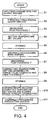
- a step S1 parameters necessary for the oxidation process using the dummy wafers (first substrates) W1 are inputted at the inputting part 42.
- the same parameters as those in a recipe for the production wafers to undergo the oxidation process for example, a gas flow rate, a pressure in the reaction tube 24, a processing time, and the like
- the operator can input the parameters one by one. Alternatively, the operator can select one recipe prepared in advance in the recipe storing part 43.
- the oxidation process to the dummy wafers W1 is started, for example by an operation at the inputting part 42 (step S2).
- the oxidation process is conducted according to the first program.
- parameters of the oxidation process other than the temperature set values, and the arrangement layout of the wafers placed on the wafer boat 3 are commonly set.
- these conditions are also used for the second and third programs as they are.
- the common arrangement layout of the wafers is not limited to that the number of the wafers and the numbers assigned for holding grooves (slots) of the wafer boat 3 are completely the same. It is sufficient that good uniformity of film thickness between surfaces can be obtained when the thermal process is conducted in accordance with a recipe.
- the dummy wafers W1 are fully arranged in the holding area for the production wafers.
- this invention is not limited to a manner wherein the wafers are arranged in the wafer boat 3 without vacancy.
- this invention is applicable to a manner wherein the production wafers are arranged in such a manner that a void area remains in the holding area for the production wafers.
- the dummy wafers W are conveyed and arranged in accordance with the arrangement layout that has been set against the wafer boat 3.
- the dummy wafers W1 are held by the wafer boat 3 in a tier-like manner in a vertical direction.
- the wafer boat 3 is conveyed into the reaction container.
- the pressure in the reaction tube 24 is reduced to a predetermined vacuum level and the thermal-processing atmosphere is heated to the respective set temperatures for the respective zones by means of the respective heaters 2 (2a to 2d).
- the O 2 (oxygen) gas and the H 2 (hydrogen) gas are supplied into the reaction tube 24 in such a manner that the inside of the reaction tube 24 is maintained at for example 0.35 Torr (about 46.6 Pa).
- the temperature of the thermal-processing atmosphere is adjusted to for example about 1000 °C.
- the respective flow rates of the first gas-supplying tubes 27b, 27c and the second gas-supplying tubes 28b, 28c are adjusted by the respective flow-rate adjusting units 27d, 27e, 28d, 28e.
- the gases are supplied only from the first gas-supplying tube 27b and the second gas-supplying tube 28b that extend to the ceiling part of the reaction tube 24.
- the O 2 gas and the H 2 gas supplied from an upper area of the wafer boat 3 are activated under the reduced-pressure and high-temperature condition to generate active species such as O-radical and/or OH-radical, and the active species flow downward.
- the oxidizing reaction proceeds on surfaces of the respective wafers.
- the dummy wafers W1 are conveyed from the longitudinal thermal processing unit to the film-thickness measuring part 6. Then, as shown in a step S3, thickness of the films on the dummy wafers W1 is measured by the film-thickness measuring part 6.
- the dummy wafers W1 are fully arranged and the thickness of the films on the dummy wafers W1 themselves is measured. However, actually, as the oxide films have been formed on the dummy wafers W1 in advance, thickness of the newly formed oxide films thereon may not be measured.
- monitor wafers that are for example bare wafers may be held in a monitor-wafer holding area that has been set at predetermine intervals among the arrangement of the dummy wafers W1, thickness of the films on the bare wafers may be measured, and the film thickness may be handled as the thickness of the films on the dummy wafers W1. Even if the monitor wafers are arranged as described above, if the dummy wafers W1 are fully arranged at the residual holding area, such arrangement is substantially the same as that the dummy wafers W1 are completely arranged at the full holding area.
- the film thickness is measured for each zone of the thermal-processing atmosphere, corresponding to each heater 2a to 2d. For example, if thicknesses of four films of the respective zones are measured, data of the film thickness T (T1, T2, T3, T4: film thickness of the dummy wafer W1 in each zone) are sent to the controlling part 4. Then, according to the first program, it is judged whether each film thickness T1 to T4 is within an error range of the target film thickness of the production wafers.
- the temperature set values of the respective heaters 2 (2a to 2d) that has been used for the present thermal process are not changed (corrected).
- the temperature set values are corrected in such a manner that the film thicknesses T1 to T4 substantially coincide with the target film thickness (step S4).
- the temperature set values based on a relationship between variation of the film thickness and variation of the temperature set values that has been obtained in advance, it is calculated how much the temperature set values should be changed from the current values in order for measured film thicknesses to substantially coincide with the target film thickness.
- the temperature set values suitable for achieving the target film thickness under the present process condition may be calculated.
- the "relationship between variation of the film thickness and variation of the temperature set values" used in the first program used is a table or the like that associates temperature with the variation of the film thickness, for example, defines how many nm the film thickness is increased or decreased by raising a temperature set value by 1 °C at a value of the measured film thickness.
- the temperature set value is corrected to y1 + (x0 - x1) ⁇ ⁇ y/ ⁇ x.
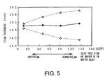
- Fig. 5 is a characteristic chart showing film-thickness profiles of wafers that have undergone the oxidation process.
- the ordinate axis represents the film thickness
- the transverse axis represents a position of wafer slot in the wafer boat 3.
- the first (leftmost) step on the transverse axis means the uppermost step
- the 140-th (rightmost) step means the lowermost step.
- the film-thickness profile shown by ⁇ is a film-thickness profile obtained by the oxidation process using dummy wafers W1 wherein the temperature set values that has been set at the step S5 were used and the target film thickness was 14.7 nm.
- the temperature set values for the respective heaters 2 (2a to 2d) are set in such a manner that the film thickness of the oxide films of each zone substantially coincides with the target film thickness.
- bare wafers W2 as the second substrates are arranged in the holding area for the production wafers W3 of the wafer boat 3.
- the oxidation process shown by a step S6 is conducted.
- the new temperature set values for the respective heater 2 (2a to 2d) stored in the previous step are used.
- Conditions other than the temperature set values are the same as those for the oxidation process in the step S2.
- the bare wafers W2 are conveyed out from the longitudinal thermal processing unit to the film-thickness measuring part 6. Then, as shown in a step S7, thickness of the films on the bare wafers W2 is measured. Thus, film thickness T' (T1', T2', T3', T4': film thickness of the bare wafer W2 in each zone) may be obtained.
- the bare wafers 2 consume more radicals because silicon is exposed on surfaces of the bare wafers. Thus, enough amounts of the radicals are not supplied to a portion on a downstream side of the process gas.
- film-thickness profile is not flat and not maintained within the vicinity of the target film thickness.
- the target film thickness is 14.7 nm, as shown in Fig. 5 by ⁇
- the film-thickness profile is lower on the right side. Maximally, the film thickness is thinner by about 0.7 to 1.0 nm.
- a correcting operation of the temperature set values is conducted as shown in a step S8. That is, the temperature set values are corrected, in such a manner that the film-thickness profile becomes substantially flat and substantially the same as the target film thickness when wafers being likely to suffer from the loading effect, such as the bare wafers W2, are used.
- the target film thicknesses of the respective zones corresponding to the respective heaters 2 (2a to 2d) are for example commonly about 14.7 nm.
- the film thicknesses T1' to T4' are lower than the target film thickness.
- differences between the film thicknesses T1' to T4' and the target film thickness are not the same.
- the film-thickness profile shown by ⁇ in Fig. 5 is about oxide films formed on the dummy wafers W1 that consume fewer radicals.
- the film-thickness profile shown by ⁇ is about oxide films formed on the bare wafers W2 that consume more radicals. In the former case, there is no or hardly any loading effect. In the latter case, there is great loading effect. That is, the difference between ⁇ and ⁇ is film-thickness difference based on the both loading effects.
- the second program determines (corrects) the temperature set values of the respective heater 2 (2a to 2d) in order to thicken the target film thicknesses of the respective zones by the differences between the present target film thickness and the film thicknesses T' to cancel the film-thickness differences based on the loading effects, that is, in order to obtain film-thickness profile shown by ⁇ in Fig. 5 about the oxide films on the dummy wafers W1.
- the respective temperature set values for the respective zones (heaters) are calculated by using the relationship between variation of the film thickness and variation of the temperature set values, which has been obtained in advance as described above.
- the corrected temperature set values are stored in the storing part 45.
- step S10 as temperature set values under the condition of the oxidation process that has been set in the step S1, the temperature set values corrected in the step S8 are written into a recipe, and the recipe is stored in the recipe storing part 43.
- step S11 the same oxidation process is conducted to the production wafers.
- an adjusting operation for temperature set values is conducted by using dummy wafers W1, which generate no or hardly any loading effect (phenomenon in which thickness of oxide films formed on wafers located on a downstream side is thinner, because oxide films on wafers consume radicals), and a thickness amount reduced from the target film thickness due to the loading effect is obtained by using bare wafers W2, which generate loading effect, and the temperature set values are raised to compensate the thickness amount, i.e., film-thickness difference due to the loading effect.
- the temperature set values are raised to compensate the thickness amount, i.e., film-thickness difference due to the loading effect.
- the adjusting operation for the temperature set values is conducted by using the oxidation process using the dummy wafers W1, which generate no or hardly any loading effect, and a difference between the film thickness and the target film thickness caused by the loading effect is measured by using the oxidation process using the bare wafers W2, which generate loading effect, and the temperature set values are adjusted again based on the difference.
- the adjusting operation for the temperature set values is conducted more easily than a trial-and-error adjusting operation for the temperature set values for example by using the production wafers W3.
- the bare wafers used in the present embodiment are used as substitutes of the production wafers.
- the wafers may have any pattern or not, and the shape of pattern is also not limited.
- the production wafers may have patterns on surfaces thereof in advance, instead of the bare wafers, the production wafers or other wafers having the same patterns may be used.
- the production wafers may be thermally processed in a state wherein the number of production wafers is smaller than the maximal number of production wafers that can be arranged in the wafer boat 3.
- a preferable embodiment suitable for such a case is explained.
- the steps S1 to S10 as shown in Fig. 4 are conducted. That is, the thermal process to the dummy wafers W1 in the step S2 of Fig.
- Fig. 6 is a view showing the present embodiment.
- the temperature set values corrected in the step S8 of Fig. 4 is stored in a storing part not shown of the controlling part 4. Then, when the thermal process to the production wafers W3 is conducted, the controlling part 4 judges the number of the production wafers W3 in one batch. The judgment is conducted by a CPU, for example based on information about the number sent from a station computer that has carried out the previous step via online, or information about the number sent from a mapping sensor provided in the thermal processing unit.
- the controlling part 4 controls the wafer-conveying unit 52 via the conveyance controller 51 in such a manner that the wafer-conveying unit 52 takes out the production wafers W3 from a wafer cassette C as shown in Fig. 2 and delivers them to the wafer boat 3.
- the production wafers W3 are arranged closely on an upstream side (upper side in this example) of the process gas supplied into the reaction container.
- the dummy wafers W1 are arranged closely in the residual holding area for the production wafers W3, to form a full-batch state.
- the wafer boat 3 is conveyed into the reaction container, the thermal process is conducted, and the oxide films are formed on the production wafers W3.
- the temperature set values stored in the storing part are used.
- process parameters other than temperature such as a pressure in the reaction container, a flow rate of the process gas, a time of the thermal process and so on, are the same as used in the thermal process to the bare wafers W2 in the step S6.
- the same film-forming result i.e. the same film thickness of the oxide films can be obtained on the production wafers, independently on the number of the production wafers W3, nevertheless the common process condition is used.
- the setting operation of the process condition is easy.
- miss in setting the process condition may be prevented.
- This invention is also applicable to other kinds of thermal processes that may generate loading effect.
- a film-forming unit by means of a chemical vapor deposition (CVD), in which dichlorosilane (SiH 2 Cl 2 ) and ammonia (NH 3 ) are used as a process gas and decomposed by giving thermal energy, and thin films of silicon nitride (SiN) are formed on wafers by means of a vapor phase reaction.
- CVD chemical vapor deposition
- an amount of the process gas consumed in the CVD may change only depending on size of grooves (size of surface area) of patterns formed on surfaces of the wafers.
- the first wafers wafers that consume a small amount of the process gas, such as dummy wafers or bare wafers having no pattern as described above, are used.
- the second wafers wafers having trenches that consume a large amount of the process gas, such as wafers having the same pattern as the production wafers, are used. Then, by using the first and second substrates, the correcting operation of the temperature set values is conducted in the same manner as the above oxidation process, so that uniformity of film thickness of the thin films formed on the production wafers may be improved between surfaces.
- the supply (flow) direction of the process gas in the heating furnace 21 is not limited to the downward direction from an upper portion of the wafer boat 3.
- the process gas may be also supplied accessorily from the first gas-supplying tube 27c and the second gas-supplying tube 28c provided at the lower portion.
- one end of the gas-discharging pipe 26 may be connected to the ceiling part of the reaction tube 2 and the process gas may be supplied only from the lower portion of the reaction tube 24, in such a manner that the flow direction of the process gas is opposite to the above embodiments (the process gas flows in an upward direction from a lower portion).
- a wafer boat which can hold 100 wafers in a holding area for production wafers, was used, dummy wafers were fully arranged in the holding area for production wafers, and an oxidation process as a thermal process was conducted.
- an area other than the holding area for production wafers of the wafer boat such as in an uppermost area and a lowermost area of the wafer boat, dummy wafers called side dummy wafers or the like were arranged.
- the temperature of the thermal-processing atmosphere means for example a set temperature at a central portion in a vertical direction of the holding area for the production wafers. Then, an adjusting operation of the temperature set values for the respective zones of the reaction container was conducted in such a manner that respective film thicknesses of monitor wafers located at the 10-th step, the 50-th step, the 80-th step and the 110-th step of the holding grooves of the wafer boat substantially coincide with a target film thickness.
- the temperature set values of the respective zones were corrected as described above in such a manner that the film thickness of the oxide films formed by the thermal process in each zone is thickened by a difference between the target film thickness of the production substrates and the film thickness shown by ⁇ . That is, the temperature set values for the respective zones were corrected in such a manner that the film thickness profile shown by ⁇ in Fig. 7 is obtained about the oxide films formed on the dummy wafers.
- the temperatures of the respective zones were set, and evaluation of the bare wafers as substitutes of the production wafers was conducted. That is, the bare wafers (bare silicon wafers) were held in the holding area for the production wafers of the wafer boat, the number of the bare wafers was variously changed, the thermal process was conducted under the same process condition, and film thickness of the oxide films on the bare wafers was measured. Specifically, the number of held bare silicon wafers was 25, 50, 75 and 100. In any of the four cases, the bare silicon wafers were closely arranged on the upstream side (upper side in this example) of the holding area for the production wafers.
- the bare silicon wafers were arranged serially downward from the 10-th uppermost step of the holding grooves of the wafer boat. Dummy wafers were arranged in the residual holding area. In any thermal process, process conditions other than the number of bare wafers were the same.
- Fig. 8 The measurement result of the film thickness is shown by Fig. 8 .
- Data shown by white marks ( ⁇ , ⁇ , ⁇ ) are film thicknesses of the oxide films on the dummy wafers.
- film thicknesses when the dummy wafers were fully arranged in the wafer holding area and the thermal process was conducted are also shown in Fig. 8 by thick short line segments.
Landscapes
- Chemical & Material Sciences (AREA)
- General Chemical & Material Sciences (AREA)
- Chemical Kinetics & Catalysis (AREA)
- Engineering & Computer Science (AREA)
- Materials Engineering (AREA)
- Mechanical Engineering (AREA)
- Metallurgy (AREA)
- Organic Chemistry (AREA)
- Formation Of Insulating Films (AREA)
Claims (17)
- Thermisches Verarbeitungsverfahren, welches thermische Verarbeitungsschritte umfasst, darunter:einen Schritt, in dem eine Mehrzahl von Substraten mit Hilfe eines Substrathalters (3) gehalten wird,einen Schritt, in dem der Substrathalter (3) in einen Reaktionsbehälter (24) transportiert wird,einen Schritt, in dem eine Mehrzahl von Zonen der thermischen Prozessatmosphäre in dem Reaktionsbehälter (24) mit Hilfe einer Mehrzahl von Heizeinheiten (2) jeweils geheizt werden, undeinen Schritt, in dem dünne Filme auf den Oberflächen der Mehrzahl von Substraten gebildet werden, indem ein Prozessgas in den Reaktionsbehälter (24) eingeführt wird, wobei das thermische Verarbeitungsverfahren folgendes umfasst:einen ersten thermischen Verarbeitungsschritt, wobei die thermischen Verarbeitungsschritte ausgeführt werden, indem eine Mehrzahl von ersten Substraten (W 1) als die Mehrzahl von Substraten verwendet wird, wobei dünne Filme auf den Oberflächen der Mehrzahl von ersten Substraten unter Verwendung eines geringeren Verbrauchs von Prozessgas gebildet werden, als auf Oberflächen von Produktionssubstraten (W3), einen ersten Messschritt, in dem eine Dicke der auf den Oberflächen der Mehrzahl von ersten Substraten (W1) ausgebildeten dünnen Filme für eine jede der Mehrzahl von Zonen der thermischen Prozessatmosphäre in dem Reaktionsbehälter (24) gemessen wird;einen ersten Einstellschritt, in dem jeweilige Temperatur-Einstellwerte der Mehrzahl von Heizeinheiten so eingestellt werden, dass die Dicke, die für eine jede der Mehrzahl von Zonen gemessen wird, im Wesentlichen mit einer Ziel-Dicke von dünnen Filmen übereinstimmt, die auf den Oberflächen von Produktions-Substraten (W3) auszubilden sind, basierend auf dem Messergebnis des ersten Messschritts;einen zweiten thermischen Verarbeitungsschritt, in dem die thermischen Verarbeitungsschritte ausgeführt werden, wobei eine Mehrzahl von zweiten Substraten (W2) als die Mehrzahl von Substraten verwendet wird, wobei dünne Filme auf den Oberflächen der Mehrzahl von zweiten Substraten (W2) unter einem höheren Verbrauch an Prozessgas ausgebildet werden, als auf den Oberflächen der Mehrzahl von ersten Substraten, und wobei die Mehrzahl von Heizeinheiten (2) jeweils auf die jeweiligen Temperatur-Einstellwerte eingestellt werden, die durch den ersten Einstellschritt eingestellt wurden;einen zweiten Messschritt, in dem eine Dicke der auf den Oberflächen der Mehrzahl von zweiten Substraten (W2) ausgebildeten dünnen Filme für eine jede der Mehrzahl von Zonen der thermischen Prozessatmosphäre in dem Reaktionsbehälter gemessen wird;einen zweiten Korrekturschritt zum Korrigieren der jeweiligen Temperatur-Einstellwerte der Mehrzahl von Heizeinheiten derart, dass die gemessene Dicke für eine jede der Mehrzahl von Zonen im Wesentlichen mit der Ziel-Dicke der dünnen Filme übereinstimmt, die auf den Oberflächen von Produktionssubstraten (W3) auszubilden sind, basierend auf dem Messergebnis des zweiten Messschrittes; undeinen dritten thermischen Verarbeitungsschritt, in dem die thermischen Verarbeitungsschritte ausgeführt werden, wobei mindestens eine Mehrzahl von Produktionssubstraten (W3) als die Mehrzahl von Substraten verwendet werden und wobei die Mehrzahl von Heizeinheiten (2) jeweils auf die jeweiligen Temperatur-Einstellwerte eingestellt werden, die durch den zweiten Korrekturschritt korrigiert wurden.
- Thermisches Verarbeitungsverfahren nach Anspruch 1, bei dem
der erste Einstellschritt und der zweite Korrekturschritt jeweils basierend auf einem Verhältnis zwischen einer Variation der Temperatur-Einstellwerte und einer Variation der Dicken der dünnen Filme ausgeführt werden, die zuvor erhalten wurde. - Thermisches Verarbeitungsverfahren nach Anspruch 1 oder 2, bei dem in den thermischen Verarbeitungsschritten das Prozessgas aktiviert wird, um aktive Spezies zu erzeugen,
und bei dem Oxidfilme auf den Oberflächen der Substrate mit Hilfe der aktiven Spezies ausgebildet werden. - Thermisches Verarbeitungsverfahren nach Anspruch 3, bei dem das Prozessgas Wasserstoffgas und Sauerstoffgas enthält.
- Thermisches Verarbeitungsverfahren nach Anspruch 3 oder 4, bei dem die ersten Substrate (W1) Substrate sind, auf denen zuvor Oxidfilme mit einer durchschnittlichen Dicke von 50 nm oder mehr ausgebildet wurden.
- Thermisches Verarbeitungsverfahren nach einem der Ansprüche 3 bis 5, bei dem die zweiten Substrate (W2) reine Siliziumsubstrate sind.
- Thermisches Verarbeitungsverfahren nach Anspruch 1 oder 2, bei dem in den thermischen Prozessschritten die dünnen Filme auf den Oberflächen der Substrate mittels chemischer Gasphasenabscheidung (CVD) ausgebildet werden.
- Thermisches Verarbeitungsverfahren nach Anspruch 7, bei dem
die ersten Substrate (W1) Substrate mit Oberflächen sind, auf denen keine Muster ausgebildet wurden, und
die zweiten Substrate (W2) Substrate mit Oberflächen sind, auf denen Muster ausgebildet wurden. - Thermisches Verarbeitungsverfahren nach einem der Ansprüche 1 bis 8, bei dem
in dem ersten thermischen Verarbeitungsschritt die ersten Substrate (W1) vollständig in einem Haltebereich für zu verarbeitende Substrate in dem Substrathalter (3) angeordnet sind, und
in dem zweiten thermischen Verarbeitungsschritt die zweiten Substrate (W2) vollständig in dem Haltebereich für zu verarbeitende Substrate in dem Substrathalter (3) angeordnet sind. - Thermisches Verarbeitungsverfahren nach Anspruch 9, bei dem
in dem dritten thermischen Verarbeitungsschritt die Produktions-Substrate (W3) in einem Abschnitt auf einer stromaufwärtigen Seite bezüglich des Flusses des Prozessgases, welches in den Reaktionsbehälter (24) eingeführt wird, in dem Haltebereich für zu bearbeitende Substrate in dem Substrathalter (3) angeordnet sind, und bei dem die ersten Substrate (W1) in dem verbleibenden Abschnitt in dem Haltebereich angeordnet sind. - Thermisches Verarbeitungsverfahren nach Anspruch 10, bei dem der Druck in dem Reaktionsbehälter (24), die Flussrate des Prozessgases und die Zeit des thermischen Prozesses in dem zweiten thermischen Verarbeitungsschritt und in dem dritten thermischen Verarbeitungsschritt identisch sind.
- Steuereinheit (4), die für eine thermische Verarbeitungseinheit verwendet wird, wobei die Steuereinheit (4) folgendes umfasst:einen Temperatur-Einstellteil, der den thermischen Prozess an einer Mehrzahl von ersten Substraten ausführt, wobei dünne Filme auf Oberflächen der Mehrzahl von ersten Substraten unter einem geringeren Verbrauch von Prozessgas ausgebildet werden, als auf den Oberflächen von Produktionssubstraten,und der die jeweiligen Temperatur-Einstellwerte der Mehrzahl von Heizeinheiten (2) der thermischen Prozesseinheit basierend auf der Dicke der dünnen Filme, die auf den Oberflächen der Mehrzahl von ersten Substraten (W1) ausgebildet werden, so einstellt, dass die gemessenen Dicken für eine jede der Mehrzahl von Zonen im Wesentlichen mit einer Ziel-Dicke der auszubildenden dünnen Filme auf den Oberflächen der Produktionssubstrate (W3) übereinstimmen, undeinen Temperatur-Korrekturteil, der den thermischen Prozess an einer Mehrzahl von zweiten Substraten (W2) gemäß den jeweiligen Temperatur-Einstellwerten durchführt, die durch den Temperatur-Einstellteil eingestellt wurden, wobei dünne Filme auf den Oberflächen der Mehrzahl von zweiten Substraten (W2) mit einem höheren Verbrauch an Prozessgas ausgebildet werden, als auf den Oberflächen der Mehrzahl von ersten Substraten (W1), und der die jeweiligen Temperatur-Einstellwerte der Mehrzahl von Heizeinheiten (2) basierend auf der Dicke der dünnen Filme, die auf den Oberflächen der Mehrzahl von zweiten Substraten (W2) ausgebildet wurden, so einstellt, dass die für eine jede der Mehrzahl von Zonen gemessene Dicke im Wesentlichen mit einer Ziel-Dicke der dünnen Filme übereinstimmt, die auf den Produktionssubstraten (W3) auszubilden sind.
- Thermische Verarbeitungseinheit, die folgendes umfasst:einen Substrathalter (3), der eine Mehrzahl von Substraten hält;einen Reaktionsbehälter (24), in den der Substrathalter transportiert wird;eine Mehrzahl von Heizeinheiten (2), die eine Mehrzahl von Zonen der thermischen Prozessatmosphäre in dem Reaktionsbehälter (24) heizt;eine Prozessgas-Einführungseinheit (27, 28), die ein Prozessgas in den Reaktionsbehälter (24) einführt, wobei das Prozessgas zum Ausbilden von dünnen Filmen auf Oberflächen einer Mehrzahl von Substraten mit Hilfe eines thermischen Prozesses dient, die Steuereinheit nach Anspruch 12; undeinen Teil für die thermische Bearbeitung von Produktionssubstraten (Fig. 3), der den thermischen Prozess an zumindest einer Mehrzahl von Produktionssubstraten (W3) gemäß den jeweiligen Temperatur-Einstellwerten durchführt, die durch den Temperatur-Korrekturteil korrigiert wurden.
- Thermische Verarbeitungseinheit nach Anspruch 13, bei der
wenn der thermische Prozess an der Mehrzahl von ersten Substraten (W1) ausgeführt wird, die ersten Substrate vollständig in einem Haltebereich für zu verarbeitende Substrate in dem Substrathalter (3) angeordnet sind, und wenn der thermische Prozess an der Mehrzahl von zweiten Substraten (W2) ausgeführt wird, die zweiten Substrate vollständig in dem Haltebereich für zu bearbeitende Substrate in dem Substrathalter (3) angeordnet sind. - Thermische Verarbeitungseinheit nach Anspruch 14, die ferner folgendes umfasst:eine Substrat-Transporteinheit, die ein Substrat auf den Substrathalter transportiert, wobei der Teil für die thermische Bearbeitung von Produktionssubstraten (Fig. 3) geeignet ist, die Substrat-Transporteinheit so zu steuern, dass dann, wenn der thermische Prozess an zumindest der Mehrzahl von Produktionssubstraten ausgeführt wird, die Produktionssubstrate in dem Haltebereich für zu bearbeitende Substrate in dem Substrathalter in einem Abschnitt auf einer stromaufwärtigen Seite eines Flusses des Prozessgases angeordnet sind, welches in den Reaktionsbehälter eingeführt wird, und die ersten Substrate in dem verbleibenden Abschnitt des Haltebereichs angeordnet sind.
- Thermische Verarbeitungseinheit nach Anspruch 15, bei der der Teil für die thermische Bearbeitung von Produktionssubstraten (Fig. 3) einen Erkennungsteil umfasst, der die Anzahl von Produktionssubstraten erkennt.
- Computerprogramm zum Steuern eines thermischen Prozesses in einer thermischen Prozesseinheit, wobei das Computerprogramm einen Programmcode umfasst, bei dessen Ausführung auf einem Computer die Steuereinheit nach Anspruch 12 implementiert wird.
Applications Claiming Priority (5)
| Application Number | Priority Date | Filing Date | Title |
|---|---|---|---|
| JP2002233513 | 2002-08-09 | ||
| JP2002233513 | 2002-08-09 | ||
| JP2003124153 | 2003-04-28 | ||
| JP2003124153A JP3853302B2 (ja) | 2002-08-09 | 2003-04-28 | 熱処理方法及び熱処理装置 |
| PCT/JP2003/010173 WO2004015750A1 (ja) | 2002-08-09 | 2003-08-08 | 熱処理方法及び熱処理装置 |
Publications (4)
| Publication Number | Publication Date |
|---|---|
| EP1548809A1 EP1548809A1 (de) | 2005-06-29 |
| EP1548809A4 EP1548809A4 (de) | 2007-02-28 |
| EP1548809B1 true EP1548809B1 (de) | 2009-12-23 |
| EP1548809B8 EP1548809B8 (de) | 2010-02-24 |
Family
ID=31719872
Family Applications (1)
| Application Number | Title | Priority Date | Filing Date |
|---|---|---|---|
| EP03784632A Expired - Lifetime EP1548809B8 (de) | 2002-08-09 | 2003-08-08 | Wàrmebehandlungsverfahren und wàrmebehandlungsvorrichtung |
Country Status (8)
| Country | Link |
|---|---|
| US (1) | US7625604B2 (de) |
| EP (1) | EP1548809B8 (de) |
| JP (1) | JP3853302B2 (de) |
| KR (1) | KR100960180B1 (de) |
| CN (1) | CN100336176C (de) |
| DE (1) | DE60330693D1 (de) |
| TW (1) | TW200406847A (de) |
| WO (1) | WO2004015750A1 (de) |
Families Citing this family (29)
| Publication number | Priority date | Publication date | Assignee | Title |
|---|---|---|---|---|
| KR100766196B1 (ko) * | 2003-08-26 | 2007-10-10 | 가부시키가이샤 히다치 고쿠사이 덴키 | 반도체 장치의 제조 방법 및 기판 처리 장치 |
| US6869892B1 (en) | 2004-01-30 | 2005-03-22 | Tokyo Electron Limited | Method of oxidizing work pieces and oxidation system |
| JP4609098B2 (ja) * | 2004-03-24 | 2011-01-12 | 東京エレクトロン株式会社 | 被処理体の酸化方法、酸化装置及び記憶媒体 |
| US20050247266A1 (en) * | 2004-05-04 | 2005-11-10 | Patel Nital S | Simultaneous control of deposition time and temperature of multi-zone furnaces |
| JP4962829B2 (ja) * | 2004-08-30 | 2012-06-27 | 信越半導体株式会社 | エピタキシャルウェーハの製造方法 |
| JP4329655B2 (ja) * | 2004-09-10 | 2009-09-09 | セイコーエプソン株式会社 | 半導体装置の製造方法及び半導体製造装置。 |
| US7700376B2 (en) * | 2005-04-06 | 2010-04-20 | Applied Materials, Inc. | Edge temperature compensation in thermal processing particularly useful for SOI wafers |
| JP4893045B2 (ja) * | 2006-03-22 | 2012-03-07 | 富士通セミコンダクター株式会社 | 薄膜製造方法及び薄膜製造装置 |
| US7951616B2 (en) * | 2006-03-28 | 2011-05-31 | Lam Research Corporation | Process for wafer temperature verification in etch tools |
| US8206996B2 (en) * | 2006-03-28 | 2012-06-26 | Lam Research Corporation | Etch tool process indicator method and apparatus |
| JP4983159B2 (ja) * | 2006-09-01 | 2012-07-25 | 東京エレクトロン株式会社 | 被処理体の酸化方法、酸化装置及び記憶媒体 |
| JP5312765B2 (ja) * | 2007-01-26 | 2013-10-09 | 株式会社日立国際電気 | 基板処理方法及び半導体製造装置 |
| JP5383332B2 (ja) | 2008-08-06 | 2014-01-08 | 株式会社日立国際電気 | 基板処理装置、基板処理方法及び半導体装置の製造方法 |
| JP5274213B2 (ja) * | 2008-11-14 | 2013-08-28 | 株式会社日立国際電気 | 基板処理装置および半導体装置の製造方法、温度制御方法 |
| JP2010147265A (ja) * | 2008-12-19 | 2010-07-01 | Hitachi Kokusai Electric Inc | 半導体装置の製造方法 |
| KR101024533B1 (ko) * | 2009-03-27 | 2011-03-31 | 주식회사 에스엠아이 | 반도체 제조설비용 히터 제어장치 및 방법 |
| JP5882918B2 (ja) * | 2010-02-24 | 2016-03-09 | ビーコ・インストゥルメンツ・インコーポレイテッド | 温度分配制御装置を用いる処理方法および処理装置 |
| JP5510897B2 (ja) * | 2010-06-07 | 2014-06-04 | 信越半導体株式会社 | エピタキシャルウェーハの製造方法 |
| US9512519B2 (en) * | 2012-12-03 | 2016-12-06 | Taiwan Semiconductor Manufacturing Company, Ltd. | Atomic layer deposition apparatus and method |
| CN103400780B (zh) * | 2013-08-14 | 2016-03-23 | 上海华力微电子有限公司 | 多晶硅炉管生长厚度监测方法 |
| JP6280407B2 (ja) * | 2014-03-19 | 2018-02-14 | 東京エレクトロン株式会社 | 基板処理方法、プログラム、制御装置、基板処理装置及び基板処理システム |
| JP6739386B2 (ja) * | 2017-03-28 | 2020-08-12 | 東京エレクトロン株式会社 | 基板処理システム、制御装置、成膜方法及びプログラム |
| JP6586440B2 (ja) * | 2017-07-11 | 2019-10-02 | 株式会社Kokusai Electric | 半導体装置の製造方法、基板処理装置およびプログラム |
| US10741426B2 (en) * | 2017-09-27 | 2020-08-11 | Taiwan Semiconductor Manufacturing Co., Ltd. | Method for controlling temperature of furnace in semiconductor fabrication process |
| JP7091227B2 (ja) * | 2018-11-05 | 2022-06-27 | 株式会社Screenホールディングス | 熱処理方法および熱処理装置 |
| US11127607B2 (en) * | 2019-11-11 | 2021-09-21 | Xia Tai Xin Semiconductor (Qing Dao) Ltd. | Heat processing system |
| JP7563844B2 (ja) * | 2020-11-06 | 2024-10-08 | 東京エレクトロン株式会社 | 熱処理装置及びダミー基板の処理方法 |
| TWI768860B (zh) * | 2021-04-29 | 2022-06-21 | 力晶積成電子製造股份有限公司 | 沉積製程控制方法 |
| CN116180223A (zh) * | 2023-01-06 | 2023-05-30 | 宁波恒普真空科技股份有限公司 | 一种可稳定控温改善晶片生长均匀性的立式成膜装置 |
Family Cites Families (12)
| Publication number | Priority date | Publication date | Assignee | Title |
|---|---|---|---|---|
| JP3070660B2 (ja) * | 1996-06-03 | 2000-07-31 | 日本電気株式会社 | 気体不純物の捕獲方法及び半導体製造装置 |
| KR100292030B1 (ko) * | 1998-09-15 | 2001-08-07 | 윤종용 | 반도체 박막 공정에서의 박막 두께 제어 방법 |
| JP2000269417A (ja) * | 1999-03-16 | 2000-09-29 | Toshiba Corp | 半導体装置 |
| JP4232307B2 (ja) * | 1999-03-23 | 2009-03-04 | 東京エレクトロン株式会社 | バッチ式熱処理装置の運用方法 |
| JP4426024B2 (ja) | 1999-09-02 | 2010-03-03 | 東京エレクトロン株式会社 | 熱処理装置の温度校正方法 |
| JP4459357B2 (ja) * | 2000-02-01 | 2010-04-28 | 東京エレクトロン株式会社 | 温度調整方法及び温度調整装置 |
| US6495805B2 (en) * | 2000-06-30 | 2002-12-17 | Tokyo Electron Limited | Method of determining set temperature trajectory for heat treatment system |
| JP3497450B2 (ja) * | 2000-07-06 | 2004-02-16 | 東京エレクトロン株式会社 | バッチ式熱処理装置及びその制御方法 |
| JP4546623B2 (ja) * | 2000-07-25 | 2010-09-15 | 東京エレクトロン株式会社 | 熱処理装置の制御条件決定方法 |
| JP2002252220A (ja) * | 2000-10-27 | 2002-09-06 | Tokyo Electron Ltd | 熱処理システム及び熱処理方法 |
| JP4222461B2 (ja) | 2000-11-07 | 2009-02-12 | 東京エレクトロン株式会社 | バッチ式熱処理方法 |
| US20030162372A1 (en) * | 2002-02-26 | 2003-08-28 | Yoo Woo Sik | Method and apparatus for forming an oxide layer |
-
2003
- 2003-04-28 JP JP2003124153A patent/JP3853302B2/ja not_active Expired - Fee Related
- 2003-08-08 TW TW092121906A patent/TW200406847A/zh not_active IP Right Cessation
- 2003-08-08 CN CNB038163764A patent/CN100336176C/zh not_active Expired - Fee Related
- 2003-08-08 US US10/523,803 patent/US7625604B2/en not_active Expired - Lifetime
- 2003-08-08 DE DE60330693T patent/DE60330693D1/de not_active Expired - Lifetime
- 2003-08-08 WO PCT/JP2003/010173 patent/WO2004015750A1/ja not_active Ceased
- 2003-08-08 EP EP03784632A patent/EP1548809B8/de not_active Expired - Lifetime
- 2003-08-08 KR KR1020047021366A patent/KR100960180B1/ko not_active Expired - Fee Related
Also Published As
| Publication number | Publication date |
|---|---|
| CN100336176C (zh) | 2007-09-05 |
| TW200406847A (en) | 2004-05-01 |
| EP1548809B8 (de) | 2010-02-24 |
| DE60330693D1 (de) | 2010-02-04 |
| JP3853302B2 (ja) | 2006-12-06 |
| TWI304617B (de) | 2008-12-21 |
| JP2004134729A (ja) | 2004-04-30 |
| CN1669127A (zh) | 2005-09-14 |
| WO2004015750A1 (ja) | 2004-02-19 |
| US7625604B2 (en) | 2009-12-01 |
| KR100960180B1 (ko) | 2010-05-26 |
| KR20050030625A (ko) | 2005-03-30 |
| EP1548809A4 (de) | 2007-02-28 |
| US20050201894A1 (en) | 2005-09-15 |
| EP1548809A1 (de) | 2005-06-29 |
Similar Documents
| Publication | Publication Date | Title |
|---|---|---|
| EP1548809B1 (de) | WûRMEBEHANDLUNGSVERFAHREN UND WûRMEBEHANDLUNGSVORRICHTUNG | |
| JP5766647B2 (ja) | 熱処理システム、熱処理方法、及び、プログラム | |
| KR100887445B1 (ko) | 기판 처리 방법 및 기판 처리 장치 | |
| US7953512B2 (en) | Substrate processing system, control method for substrate processing apparatus and program stored on medium | |
| US20090124083A1 (en) | Film formation apparatus and method for using same | |
| JP2009044023A (ja) | 半導体装置の製造方法および基板処理装置 | |
| JP5049303B2 (ja) | 熱処理装置、熱処理装置の温度調整方法、及び、プログラム | |
| KR20180100630A (ko) | 반도체 장치의 제조 방법, 기판 장전 방법 및 기록 매체 | |
| US8354135B2 (en) | Thermal processing apparatus, method for regulating temperature of thermal processing apparatus, and program | |
| JP6596316B2 (ja) | 熱処理システム、熱処理方法、及び、プログラム | |
| US20140090594A1 (en) | Thin film forming apparatus and computer-readable medium | |
| CN107236936A (zh) | 控制装置、基板处理系统、基板处理方法以及存储介质 | |
| CN114256092A (zh) | 半导体器件的制造方法、衬底处理装置及记录介质 | |
| JP5049302B2 (ja) | 熱処理装置、熱処理装置の温度調整方法、及び、プログラム | |
| US20060099805A1 (en) | Heat treating system and heat treating method | |
| US20020127828A1 (en) | Method of processing wafer | |
| JP4553227B2 (ja) | 熱処理方法 | |
| TWI871487B (zh) | 基板處理方法、半導體裝置之製造方法、程式及基板處理裝置 | |
| TWI433239B (zh) | 熱處理裝置、熱處理裝置之溫度調整方法、及程式 | |
| KR20200107762A (ko) | 기판 처리 장치, 반도체 장치의 제조 방법 및 기록 매체 | |
| US20240170310A1 (en) | Substrate processing apparatus, method of manufacturing semiconductor device, and recording medium | |
| JPWO2020188632A1 (ja) | 半導体装置の製造方法、基板処理方法、プログラムおよび基板処理装置 | |
| JPH11329979A (ja) | 化学気相成長装置および化学気相成長法 | |
| US11581200B2 (en) | Method of manufacturing semiconductor device, substrate processing apparatus, and recording medium | |
| JP2001338883A (ja) | 半導体装置の製造方法 |
Legal Events
| Date | Code | Title | Description |
|---|---|---|---|
| PUAI | Public reference made under article 153(3) epc to a published international application that has entered the european phase |
Free format text: ORIGINAL CODE: 0009012 |
|
| 17P | Request for examination filed |
Effective date: 20050210 |
|
| AK | Designated contracting states |
Kind code of ref document: A1 Designated state(s): AT BE BG CH CY CZ DE DK EE ES FI FR GB GR HU IE IT LI LU MC NL PT RO SE SI SK TR |
|
| RBV | Designated contracting states (corrected) |
Designated state(s): DE FR GB IT NL |
|
| A4 | Supplementary search report drawn up and despatched |
Effective date: 20070131 |
|
| RIC1 | Information provided on ipc code assigned before grant |
Ipc: H01L 21/31 20060101ALI20070125BHEP Ipc: H01L 21/00 20060101ALI20070125BHEP Ipc: H01L 21/205 20060101AFI20040303BHEP |
|
| 17Q | First examination report despatched |
Effective date: 20080314 |
|
| GRAP | Despatch of communication of intention to grant a patent |
Free format text: ORIGINAL CODE: EPIDOSNIGR1 |
|
| GRAS | Grant fee paid |
Free format text: ORIGINAL CODE: EPIDOSNIGR3 |
|
| GRAA | (expected) grant |
Free format text: ORIGINAL CODE: 0009210 |
|
| AK | Designated contracting states |
Kind code of ref document: B1 Designated state(s): DE FR GB IT NL |
|
| REG | Reference to a national code |
Ref country code: GB Ref legal event code: FG4D |
|
| REF | Corresponds to: |
Ref document number: 60330693 Country of ref document: DE Date of ref document: 20100204 Kind code of ref document: P |
|
| PLBE | No opposition filed within time limit |
Free format text: ORIGINAL CODE: 0009261 |
|
| STAA | Information on the status of an ep patent application or granted ep patent |
Free format text: STATUS: NO OPPOSITION FILED WITHIN TIME LIMIT |
|
| 26N | No opposition filed |
Effective date: 20100924 |
|
| PG25 | Lapsed in a contracting state [announced via postgrant information from national office to epo] |
Ref country code: IT Free format text: LAPSE BECAUSE OF FAILURE TO SUBMIT A TRANSLATION OF THE DESCRIPTION OR TO PAY THE FEE WITHIN THE PRESCRIBED TIME-LIMIT Effective date: 20091223 |
|
| GBPC | Gb: european patent ceased through non-payment of renewal fee |
Effective date: 20100808 |
|
| PG25 | Lapsed in a contracting state [announced via postgrant information from national office to epo] |
Ref country code: GB Free format text: LAPSE BECAUSE OF NON-PAYMENT OF DUE FEES Effective date: 20100808 |
|
| REG | Reference to a national code |
Ref country code: FR Ref legal event code: PLFP Year of fee payment: 13 |
|
| PGFP | Annual fee paid to national office [announced via postgrant information from national office to epo] |
Ref country code: NL Payment date: 20150709 Year of fee payment: 13 |
|
| PGFP | Annual fee paid to national office [announced via postgrant information from national office to epo] |
Ref country code: DE Payment date: 20150804 Year of fee payment: 13 |
|
| PGFP | Annual fee paid to national office [announced via postgrant information from national office to epo] |
Ref country code: FR Payment date: 20150629 Year of fee payment: 13 |
|
| REG | Reference to a national code |
Ref country code: DE Ref legal event code: R119 Ref document number: 60330693 Country of ref document: DE |
|
| REG | Reference to a national code |
Ref country code: NL Ref legal event code: MM Effective date: 20160901 |
|
| REG | Reference to a national code |
Ref country code: FR Ref legal event code: ST Effective date: 20170428 |
|
| PG25 | Lapsed in a contracting state [announced via postgrant information from national office to epo] |
Ref country code: NL Free format text: LAPSE BECAUSE OF NON-PAYMENT OF DUE FEES Effective date: 20160901 |
|
| PG25 | Lapsed in a contracting state [announced via postgrant information from national office to epo] |
Ref country code: FR Free format text: LAPSE BECAUSE OF NON-PAYMENT OF DUE FEES Effective date: 20160831 Ref country code: DE Free format text: LAPSE BECAUSE OF NON-PAYMENT OF DUE FEES Effective date: 20170301 |