EP1548850B1 - Dispositif d'emission de lumiere blanche - Google Patents
Dispositif d'emission de lumiere blanche Download PDFInfo
- Publication number
- EP1548850B1 EP1548850B1 EP03799123A EP03799123A EP1548850B1 EP 1548850 B1 EP1548850 B1 EP 1548850B1 EP 03799123 A EP03799123 A EP 03799123A EP 03799123 A EP03799123 A EP 03799123A EP 1548850 B1 EP1548850 B1 EP 1548850B1
- Authority
- EP
- European Patent Office
- Prior art keywords
- light
- light emitting
- phosphor
- red
- green
- Prior art date
- Legal status (The legal status is an assumption and is not a legal conclusion. Google has not performed a legal analysis and makes no representation as to the accuracy of the status listed.)
- Expired - Lifetime
Links
Images


Classifications
-
- C—CHEMISTRY; METALLURGY
- C09—DYES; PAINTS; POLISHES; NATURAL RESINS; ADHESIVES; COMPOSITIONS NOT OTHERWISE PROVIDED FOR; APPLICATIONS OF MATERIALS NOT OTHERWISE PROVIDED FOR
- C09K—MATERIALS FOR MISCELLANEOUS APPLICATIONS, NOT PROVIDED FOR ELSEWHERE
- C09K11/00—Luminescent materials, e.g. electroluminescent or chemiluminescent
- C09K11/08—Luminescent materials, e.g. electroluminescent or chemiluminescent containing inorganic luminescent materials
- C09K11/77—Luminescent materials, e.g. electroluminescent or chemiluminescent containing inorganic luminescent materials containing rare earth metals
- C09K11/7728—Luminescent materials, e.g. electroluminescent or chemiluminescent containing inorganic luminescent materials containing rare earth metals containing europium
- C09K11/7735—Germanates
-
- C—CHEMISTRY; METALLURGY
- C09—DYES; PAINTS; POLISHES; NATURAL RESINS; ADHESIVES; COMPOSITIONS NOT OTHERWISE PROVIDED FOR; APPLICATIONS OF MATERIALS NOT OTHERWISE PROVIDED FOR
- C09K—MATERIALS FOR MISCELLANEOUS APPLICATIONS, NOT PROVIDED FOR ELSEWHERE
- C09K11/00—Luminescent materials, e.g. electroluminescent or chemiluminescent
- C09K11/08—Luminescent materials, e.g. electroluminescent or chemiluminescent containing inorganic luminescent materials
- C09K11/77—Luminescent materials, e.g. electroluminescent or chemiluminescent containing inorganic luminescent materials containing rare earth metals
- C09K11/7728—Luminescent materials, e.g. electroluminescent or chemiluminescent containing inorganic luminescent materials containing rare earth metals containing europium
- C09K11/7729—Chalcogenides
- C09K11/7731—Chalcogenides with alkaline earth metals
-
- C—CHEMISTRY; METALLURGY
- C09—DYES; PAINTS; POLISHES; NATURAL RESINS; ADHESIVES; COMPOSITIONS NOT OTHERWISE PROVIDED FOR; APPLICATIONS OF MATERIALS NOT OTHERWISE PROVIDED FOR
- C09K—MATERIALS FOR MISCELLANEOUS APPLICATIONS, NOT PROVIDED FOR ELSEWHERE
- C09K11/00—Luminescent materials, e.g. electroluminescent or chemiluminescent
- C09K11/08—Luminescent materials, e.g. electroluminescent or chemiluminescent containing inorganic luminescent materials
- C09K11/77—Luminescent materials, e.g. electroluminescent or chemiluminescent containing inorganic luminescent materials containing rare earth metals
- C09K11/7728—Luminescent materials, e.g. electroluminescent or chemiluminescent containing inorganic luminescent materials containing rare earth metals containing europium
- C09K11/77344—Aluminosilicates
-
- C—CHEMISTRY; METALLURGY
- C09—DYES; PAINTS; POLISHES; NATURAL RESINS; ADHESIVES; COMPOSITIONS NOT OTHERWISE PROVIDED FOR; APPLICATIONS OF MATERIALS NOT OTHERWISE PROVIDED FOR
- C09K—MATERIALS FOR MISCELLANEOUS APPLICATIONS, NOT PROVIDED FOR ELSEWHERE
- C09K11/00—Luminescent materials, e.g. electroluminescent or chemiluminescent
- C09K11/08—Luminescent materials, e.g. electroluminescent or chemiluminescent containing inorganic luminescent materials
- C09K11/77—Luminescent materials, e.g. electroluminescent or chemiluminescent containing inorganic luminescent materials containing rare earth metals
- C09K11/7728—Luminescent materials, e.g. electroluminescent or chemiluminescent containing inorganic luminescent materials containing rare earth metals containing europium
- C09K11/7737—Phosphates
-
- C—CHEMISTRY; METALLURGY
- C09—DYES; PAINTS; POLISHES; NATURAL RESINS; ADHESIVES; COMPOSITIONS NOT OTHERWISE PROVIDED FOR; APPLICATIONS OF MATERIALS NOT OTHERWISE PROVIDED FOR
- C09K—MATERIALS FOR MISCELLANEOUS APPLICATIONS, NOT PROVIDED FOR ELSEWHERE
- C09K11/00—Luminescent materials, e.g. electroluminescent or chemiluminescent
- C09K11/08—Luminescent materials, e.g. electroluminescent or chemiluminescent containing inorganic luminescent materials
- C09K11/77—Luminescent materials, e.g. electroluminescent or chemiluminescent containing inorganic luminescent materials containing rare earth metals
- C09K11/7728—Luminescent materials, e.g. electroluminescent or chemiluminescent containing inorganic luminescent materials containing rare earth metals containing europium
- C09K11/774—Borates
-
- H—ELECTRICITY
- H10—SEMICONDUCTOR DEVICES; ELECTRIC SOLID-STATE DEVICES NOT OTHERWISE PROVIDED FOR
- H10H—INORGANIC LIGHT-EMITTING SEMICONDUCTOR DEVICES HAVING POTENTIAL BARRIERS
- H10H20/00—Individual inorganic light-emitting semiconductor devices having potential barriers, e.g. light-emitting diodes [LED]
- H10H20/80—Constructional details
- H10H20/85—Packages
- H10H20/851—Wavelength conversion means
- H10H20/8511—Wavelength conversion means characterised by their material, e.g. binder
- H10H20/8512—Wavelength conversion materials
-
- H—ELECTRICITY
- H10—SEMICONDUCTOR DEVICES; ELECTRIC SOLID-STATE DEVICES NOT OTHERWISE PROVIDED FOR
- H10H—INORGANIC LIGHT-EMITTING SEMICONDUCTOR DEVICES HAVING POTENTIAL BARRIERS
- H10H20/00—Individual inorganic light-emitting semiconductor devices having potential barriers, e.g. light-emitting diodes [LED]
- H10H20/80—Constructional details
- H10H20/85—Packages
- H10H20/851—Wavelength conversion means
- H10H20/8511—Wavelength conversion means characterised by their material, e.g. binder
- H10H20/8512—Wavelength conversion materials
- H10H20/8513—Wavelength conversion materials having two or more wavelength conversion materials
-
- H—ELECTRICITY
- H10—SEMICONDUCTOR DEVICES; ELECTRIC SOLID-STATE DEVICES NOT OTHERWISE PROVIDED FOR
- H10W—GENERIC PACKAGES, INTERCONNECTIONS, CONNECTORS OR OTHER CONSTRUCTIONAL DETAILS OF DEVICES COVERED BY CLASS H10
- H10W72/00—Interconnections or connectors in packages
- H10W72/071—Connecting or disconnecting
- H10W72/072—Connecting or disconnecting of bump connectors
- H10W72/07251—Connecting or disconnecting of bump connectors characterised by changes in properties of the bump connectors during connecting
- H10W72/07252—Connecting or disconnecting of bump connectors characterised by changes in properties of the bump connectors during connecting changes in structures or sizes
-
- H—ELECTRICITY
- H10—SEMICONDUCTOR DEVICES; ELECTRIC SOLID-STATE DEVICES NOT OTHERWISE PROVIDED FOR
- H10W—GENERIC PACKAGES, INTERCONNECTIONS, CONNECTORS OR OTHER CONSTRUCTIONAL DETAILS OF DEVICES COVERED BY CLASS H10
- H10W72/00—Interconnections or connectors in packages
- H10W72/071—Connecting or disconnecting
- H10W72/075—Connecting or disconnecting of bond wires
- H10W72/07551—Connecting or disconnecting of bond wires characterised by changes in properties of the bond wires during the connecting
- H10W72/07554—Connecting or disconnecting of bond wires characterised by changes in properties of the bond wires during the connecting changes in dispositions
-
- H—ELECTRICITY
- H10—SEMICONDUCTOR DEVICES; ELECTRIC SOLID-STATE DEVICES NOT OTHERWISE PROVIDED FOR
- H10W—GENERIC PACKAGES, INTERCONNECTIONS, CONNECTORS OR OTHER CONSTRUCTIONAL DETAILS OF DEVICES COVERED BY CLASS H10
- H10W72/00—Interconnections or connectors in packages
- H10W72/20—Bump connectors, e.g. solder bumps or copper pillars; Dummy bumps; Thermal bumps
- H10W72/221—Structures or relative sizes
- H10W72/227—Multiple bumps having different sizes
-
- H—ELECTRICITY
- H10—SEMICONDUCTOR DEVICES; ELECTRIC SOLID-STATE DEVICES NOT OTHERWISE PROVIDED FOR
- H10W—GENERIC PACKAGES, INTERCONNECTIONS, CONNECTORS OR OTHER CONSTRUCTIONAL DETAILS OF DEVICES COVERED BY CLASS H10
- H10W72/00—Interconnections or connectors in packages
- H10W72/50—Bond wires
- H10W72/541—Dispositions of bond wires
- H10W72/547—Dispositions of multiple bond wires
-
- H—ELECTRICITY
- H10—SEMICONDUCTOR DEVICES; ELECTRIC SOLID-STATE DEVICES NOT OTHERWISE PROVIDED FOR
- H10W—GENERIC PACKAGES, INTERCONNECTIONS, CONNECTORS OR OTHER CONSTRUCTIONAL DETAILS OF DEVICES COVERED BY CLASS H10
- H10W72/00—Interconnections or connectors in packages
- H10W72/851—Dispositions of multiple connectors or interconnections
- H10W72/874—On different surfaces
- H10W72/884—Die-attach connectors and bond wires
-
- H—ELECTRICITY
- H10—SEMICONDUCTOR DEVICES; ELECTRIC SOLID-STATE DEVICES NOT OTHERWISE PROVIDED FOR
- H10W—GENERIC PACKAGES, INTERCONNECTIONS, CONNECTORS OR OTHER CONSTRUCTIONAL DETAILS OF DEVICES COVERED BY CLASS H10
- H10W72/00—Interconnections or connectors in packages
- H10W72/90—Bond pads, in general
-
- H—ELECTRICITY
- H10—SEMICONDUCTOR DEVICES; ELECTRIC SOLID-STATE DEVICES NOT OTHERWISE PROVIDED FOR
- H10W—GENERIC PACKAGES, INTERCONNECTIONS, CONNECTORS OR OTHER CONSTRUCTIONAL DETAILS OF DEVICES COVERED BY CLASS H10
- H10W72/00—Interconnections or connectors in packages
- H10W72/90—Bond pads, in general
- H10W72/941—Dispositions of bond pads
- H10W72/9415—Dispositions of bond pads relative to the surface, e.g. recessed, protruding
-
- H—ELECTRICITY
- H10—SEMICONDUCTOR DEVICES; ELECTRIC SOLID-STATE DEVICES NOT OTHERWISE PROVIDED FOR
- H10W—GENERIC PACKAGES, INTERCONNECTIONS, CONNECTORS OR OTHER CONSTRUCTIONAL DETAILS OF DEVICES COVERED BY CLASS H10
- H10W72/00—Interconnections or connectors in packages
- H10W72/90—Bond pads, in general
- H10W72/941—Dispositions of bond pads
- H10W72/944—Dispositions of multiple bond pads
-
- H—ELECTRICITY
- H10—SEMICONDUCTOR DEVICES; ELECTRIC SOLID-STATE DEVICES NOT OTHERWISE PROVIDED FOR
- H10W—GENERIC PACKAGES, INTERCONNECTIONS, CONNECTORS OR OTHER CONSTRUCTIONAL DETAILS OF DEVICES COVERED BY CLASS H10
- H10W90/00—Package configurations
-
- H—ELECTRICITY
- H10—SEMICONDUCTOR DEVICES; ELECTRIC SOLID-STATE DEVICES NOT OTHERWISE PROVIDED FOR
- H10W—GENERIC PACKAGES, INTERCONNECTIONS, CONNECTORS OR OTHER CONSTRUCTIONAL DETAILS OF DEVICES COVERED BY CLASS H10
- H10W90/00—Package configurations
- H10W90/701—Package configurations characterised by the relative positions of pads or connectors relative to package parts
- H10W90/721—Package configurations characterised by the relative positions of pads or connectors relative to package parts of bump connectors
- H10W90/722—Package configurations characterised by the relative positions of pads or connectors relative to package parts of bump connectors between stacked chips
-
- H—ELECTRICITY
- H10—SEMICONDUCTOR DEVICES; ELECTRIC SOLID-STATE DEVICES NOT OTHERWISE PROVIDED FOR
- H10W—GENERIC PACKAGES, INTERCONNECTIONS, CONNECTORS OR OTHER CONSTRUCTIONAL DETAILS OF DEVICES COVERED BY CLASS H10
- H10W90/00—Package configurations
- H10W90/701—Package configurations characterised by the relative positions of pads or connectors relative to package parts
- H10W90/731—Package configurations characterised by the relative positions of pads or connectors relative to package parts of die-attach connectors
- H10W90/736—Package configurations characterised by the relative positions of pads or connectors relative to package parts of die-attach connectors between a chip and a stacked lead frame, conducting package substrate or heat sink
-
- H—ELECTRICITY
- H10—SEMICONDUCTOR DEVICES; ELECTRIC SOLID-STATE DEVICES NOT OTHERWISE PROVIDED FOR
- H10W—GENERIC PACKAGES, INTERCONNECTIONS, CONNECTORS OR OTHER CONSTRUCTIONAL DETAILS OF DEVICES COVERED BY CLASS H10
- H10W90/00—Package configurations
- H10W90/701—Package configurations characterised by the relative positions of pads or connectors relative to package parts
- H10W90/751—Package configurations characterised by the relative positions of pads or connectors relative to package parts of bond wires
- H10W90/756—Package configurations characterised by the relative positions of pads or connectors relative to package parts of bond wires between a chip and a stacked lead frame, conducting package substrate or heat sink
-
- Y—GENERAL TAGGING OF NEW TECHNOLOGICAL DEVELOPMENTS; GENERAL TAGGING OF CROSS-SECTIONAL TECHNOLOGIES SPANNING OVER SEVERAL SECTIONS OF THE IPC; TECHNICAL SUBJECTS COVERED BY FORMER USPC CROSS-REFERENCE ART COLLECTIONS [XRACs] AND DIGESTS
- Y02—TECHNOLOGIES OR APPLICATIONS FOR MITIGATION OR ADAPTATION AGAINST CLIMATE CHANGE
- Y02B—CLIMATE CHANGE MITIGATION TECHNOLOGIES RELATED TO BUILDINGS, e.g. HOUSING, HOUSE APPLIANCES OR RELATED END-USER APPLICATIONS
- Y02B20/00—Energy efficient lighting technologies, e.g. halogen lamps or gas discharge lamps
Definitions
- the present invention relates to a white light emitting device having a light emitting element and phosphors to emit a white light, and which is applied to, for example, an LED display, a backlight device, a signal device, an illumination type switch, a variety of sensors, a variety of indicators and the like.
- a light emitting element used for a light emitting device includes an inorganic LED (Light Emitting Diode), an organic LED, a laser diode, an inorganic thick film electroluminescence sheet or an inorganic thin film electroluminescence parts and the like.
- LED stands out in characteristics such as long life, space-saving, good resistance to impact shock, and further, capable of emitting a light in a narrow spectral band.
- a number of luminous colors i.e. a number of luminous colors in a particularly wide spectral band cannot be realized or can be realized only in an inefficient manner by light emission inherent to an active semiconductor material in LED. Especially, such tendency is remarkable in case of white light emission.
- a luminous color which cannot be essentially realized is attained by a wavelength conversion technique.
- the wavelength conversion technique is essentially based on the following principle. Namely, at least one phosphor is placed on an LED, and the light emitted from the LED is absorbed by the phosphor to emit a light having a wavelength different from that of the light absorbed. In other words, a light emitted is absorbed by an LED, and then, a photoluminescence light is radiated with another luminous color.
- red/green/blue phosphors respective colors of red/green/blue (hereinafter referred to as "red/green/blue phosphors in case of expressing collectively) which are in practical use at present, to emit a light is well known.
- red/green/blue phosphors respective colors of red/green/blue
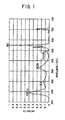
- FIG. 1 is a spectral diagram indicating emission intensity of a conventional white LED lamp. As shown in the figure, since there is scarcely a yellow component having a wavelength of 560 to 590 nm, an average color rendering evaluation number Ra of the white LED lamp is as low as about 50 to 60. In a usual fluorescent lamp, an average color rendering evaluation number Ra is about 80 to 90, and ideal is 100.
- Document WO02/054502 discloses a light source comprising a light-emitting element which emits light in a first spectral region, and comprises a luminophore, which comes from the group of alkaline-earth orthosilicates and which absorbs a portion of the light emitted by the light source and emits light in another spectral region.
- the luminophore is an alkaline-earth orthosilicate, which is activated with bivalent europium and whose composition consists of: (2-x-y) SrO x (Ba, Ca) O (1-a-b-c-d) SiO 2 aP 2 O 5 bAl 2 O 3 cB 2 O 3 dGeO 2 : y Eu 2+ and/or (2-x-y) BaO x ((Sr, Ca) O (1-a-b-c-d) SiO 2 aP 2 O 5 bAl 2 O 3 cB 2 O 3 dGeO 2 : y Eu 2+ .
- the desired color can be easily adjusted by using a luminophore of the aforementioned type.
- the light source can contain an additional luminophore selected from the group of alkaline-earth aluminates, activated with bivalent europium and/or manganese, and/or can contain an additional red-emitting luminophore selected from the group Y(V, P, Si)O 4 :Eu or can contain alkaline-earth magnesium disilicate.
- document EP 1 107 321 discloses a light emitting diode comprising a light emitting diode element mounted on a glass epoxy substrate, this light emitting diode element being protected at its surface side by a resin seal member, in which: a light emitting diode element for blue luminescence, formed of gallium nitride type compound semiconductor is used as the above-mentioned light emitting diode element; and a fluorescent material containing layer composed of a fluorescent material dispersed into an adhesive is arranged on the back side of this light emitting diode element. On the back side of the light emitting diode element, blue luminescence is converted in wavelength to produce white luminescence of high intensity.
- An object of the present invention is to provide a white light emitting device having improved color rendering properties.
- a white light emitting device in provided in which color deviation is hard to appear.
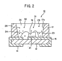
- FIG. 2 is a sectional view showing a white LED lamp according to a first embodiment of the present invention.
- the white LED lamp 10 shown in FIG. 2 is an SMD (Surface Mounted Device) type, and has the following structure. Electrically insulated two lead frames 14 and 15 are formed on the upper, lower and side surfaces of an insulative glass-epoxy resin substrate 12 in a gold pattern, and a frame 17 made of a plastic and having a cup 17a is disposed on the lead frames 14 and 15. A surface of the cup 17a is a reflecting mirror reflecting a light emitted from a purple LED 19.
- the lead frames 14 and 15 are asymmetrical to each other wherein the upper surface of the lead frame 15 is formed beyond a central portion of the bottom of a space provided by the cup 17a of the frame 17, while the other lead frame 14 is formed to somewhat expose into the bottom of the space.
- the purple LED 19 emits a purple light of 395 nm, and fixed to the upper surface of the lead frame 15 by a mount 21 prepared from a silver filler-containing epoxy resin paste and the like. In this case, however, the purple LED 19 may be replaced by another LED emitting any of lights in a wavelength region of 350 to 400 nm.
- a p-electrode of the purple LED 19 is connected to the lead frame 15 through a gold bonding wire 23, while an n-electrode of the purple LED 19 is connected to the lead frame 14 through a gold bonding wire 24.
- the space formed in the frame 17 is filled with a sealant 26 which comes to be transparent after being cured, and the purple LED 19 is secured with the sealant 26.
- the sealant 26 is made of silicone resin or epoxy resin, and the sealant 26 is mixed with a yellow phosphor 31 being a characteristic element of the present invention (which will be described in detail hereinafter) in addition to a red phosphor 28, a green phosphor 29; and a blue phosphor 30 which are explained in a conventional example.
- either the sealant 26 into which the red, green, blue, and yellow phosphors 28 to 31 are mixed may fill up the whole space in the cup 17a formed in the frame 17, or it may fill up a section extending from the upper edge of the frame 17 to a region positioned under the upper edge.
- a diffusion material diffusing a light may be mixed into the sealant 26 admixed with the red, green, blue, and yellow phosphors 28 to 31.
- a light emitted from the purple LED 19 is reflected diffusely by the diffusion material to become a scattered light, so that the light emitted from the purple LED strikes easily on the red, green, and yellow phosphors 28 to 31, whereby light intensity of the light radiated from the red, green, blue, and yellow phosphors 28 to 31 increases.
- the diffusion material is not specifically limited, but well-known materials may be used.
- the yellow phosphor 31 is radiated as a result of subjecting 395 nm wavelength of a purple light emitted from the purple LED 19 to wavelength conversion into 560 to 590 nm wavelength of a yellow light.
- a mixing ratio is desirable to be around 5% in volume ratio with respect to the whole volume of the mixture including the sealant 26.
- the yellow phosphor 31 is made of an alkaline earth metal orthosilicate activated with divalent europium.
- the yellow phosphor 31 may be an alkaline earth metal orthosilicate activated with divalent europium represented by a formula:
- Emission spectrum is influenced by a substitution of germanium for a silicon part, and P 2 O 3 , Al 2 O 3 and/or B 2 O 3 existing additionally, so that the emission spectrum may be adjusted most suitably in case of applying the respective components.
- the phosphor 31 has another phosphor selected from the group of alkaline earth metal aluminates activated with divalent europium and/or manganese and/or Y (V, P, Si) O 4 :Eu or a further phosphor emitting a light having a color near to red selected from the group of alkaline earth metal-magnesium-disilicate: E U 2+ . Mn 2+ represented by the following formula:
- a monovalent ion, particularly a halide is incorporated into a phosphor lattice, it is advantageous as to degree of crystallization and emissivity. It is advantageous that a spectral range is in 300 to 500 nm. In such wavelength region, the yellow phosphor 31 is well excited.
- silicate phosphor For the fabrication of a silicate phosphor, stoichiometric amounts of starting materials of alkaline earth metal carbonate, silicon dioxide, and europium oxide are intimately mixed with each other in response to a selected composition, and the mixture is converted into a desired phosphor at temperatures of 1100°C and 1400°C under the reducing atmosphere in accordance with a solid state reaction for the fabrication of phosphor in common use.
- a part of silicon may be replaced by germanium, boron, aluminum, phosphor, and a part of europium may be replaced by manganese.
- the operation is made by addition of corresponding amounts of compounds of the above-described elements which are thermally decomposed into oxides. In this case, a range of the reaction conditions is maintained.
- the resulting silicate emits a light having a wavelength of 10 nm to 600 nm, and has a half value width of up to 110 nm.
- Luminous colors having defined color temperatures and high color reproducibility can be obtained by the use of any one of phosphors from the above-described groups or phosphors obtained by combining those from the above-described groups, or alkaline earth metal aluminates activated with divalent europium and/or manganese, further additional phosphors emitting a light having a color near to red from a group of Y (V, P, Si)O 4 :Eu 2+ Y 2 O 2 S:Eu 3+ , and a combination of phosphors from the groups with phosphors in common use.
- the fact is as shown in the following examples:
- a resin used for the mount 21 has adhesiveness, besides the resin preferably is electrically insulative in such that even when the mount 21 rises along sides of the purple LED 19 having a very small shape, the respective layers do not short-circuit between them.
- the mount 21 permits the light emitted isotropically from the purple LED 19 to be pervious, and to reflect the light by a reflecting mirror on a surface of the cup 17a, then the light reflected is emitted upwards the white LED lamp 10. For this reason, a transparent resin is used for the mount. In this case, since the white LED lamp 10 is a white light source, the mount 21 may have white color which does not interfere with a white light.
- the red/green/blue/yellow phosphors 28 to 31 may be contained in the mount 21. Since the purple LED 19 emits a slight isotropically, and the light is reflected also by a surface of the cup 17a, these lights transmit through the mount 21, so that optical density is extremely high in the mount 21. In this respect, when the red/green/blue/yellow phosphors 28 to 31 are contained in the mount 21, the light emitted from the purple LED 19 is reflected by the red/green/blue/yellow phosphors 28 to 31 in the mount 21, and on one hand, a light is newly emitted isotropically as that excited by the red/green/blue/yellow phosphors 28 to 31 in the mount 21. As described above, when the red/green/blue/yellow phosphors 28 to 31 are also contained in the mount 21, the white LED lamp 10 becomes further high luminous.
- a resin containing an inorganic material such as Ag may be used for the mount 21.
- the mount 21 or the sealant 26 made of a synthetic resin disposed at the very vicinity of the purple LED 19 is colored in brown or black, resulting in deterioration, whereby its luminous efficiency decreases.
- a resin such as silicone resin, and epoxy resin is used for the mount 21 and the sealant 26.
- particularly coloring of the mount 21 at the vicinity of the purple LED 19 reducers remarkably its luminous efficiency.
- the mount 21 is required to have not only weatherability against deterioration of the resin due to a light from the purple LED 19, but also adhesiveness, adhesion and the like.
- Such deterioration of resin due to a light may be solved by employing a resin containing an inorganic material such as Ag in the mount 21.
- a resin containing an inorganic material such as Ag in the mount 21.
- Such mount 21 can be easily formed by admixing an Ag paste and the red/green/blue/yellow phosphors 28 to 31 with a mounting paste, applying the resulting admixture on the lead frame 15 by mounting equipment, and the purple LED 19 is bonded hereto.
- silicone resin containing an inorganic material may be used as an organic resin for the mount 21 other than the epoxy resin containing Ag.
- an inorganic material used in the mount 21 it is required to have good adhesion with respect to a resin, and no deterioration by the light from the purple LED 19.
- at least one inorganic material selected from silver, gold, aluminum, copper, alumina, silica, titanium oxide, boron nitride, tin oxide, zinc oxide, and ITO is contained in a resin.
- silver, gold, aluminum, copper and the like make heat dissipation properties better, besides exhibit electroconductivity, so that they are applicable for semiconductor device which expects electroconductivity.
- alumina, silica, titanium oxide and the like exhibit high weatherability, so that high reflection coefficient can be maintained by them.
- Inorganic materials may have a variety of forms such as spherical, needle-, flake-formed and the like forms with taking dispersion properties, electroconductivity and the like into consideration.
- a content of an inorganic material in a resin of the mount 21 may be adjusted variously in accordance with heat dissipating properties, electroconductivity and the like desired.
- adhesive properties decrease.
- it is arranged in such that the content ranges from 5% by weight or more to 80% by weight or less. In this respect, however, when the content is to be from 60% by weight or more to 80% by weight or more, deterioration, of a resin can be more suitably prevented.
- luminance of the white LED lamp 10 can be more elevated.
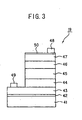
- FIG. 3 shows a layer structure of the purple LED 19 wherein the purple LED 19 has, for example, a sapphire substrate 41 as a transparent substrate.
- nitride semiconductor layers for example, a buffer layer 42, an n-type contact layer 43, an n-type cladding layer 44, an MQW (multi-quantum well) active layer 45, a p-type cladding layer 46, and a p-type contact layer 47 are sequentially formed in accordance with MOCVD method or the like.
- a transmittive electrode 50 is formed on the whole surface of the p-type contact layer 47, a p-electrode 46 is formed on a part of the transmittive electrode 50, and an n-electrode 49 is formed on a part of the n-type contact layer 43 in accordance with sputtering method, vacuum evaporation technique or the like.
- the buffer layer 42 is made of, for example, AlN, and the n-type contact layer is made of, for example. GaN.
- the n-type cladding layer 44 is made of, for example, Al y Ga 1-y N (0 ⁇ y ⁇ 1)
- the p-type cladding layer is made of, for example, Al x Ga 1-x N (0 ⁇ x ⁇ 1)
- the p-type contact layer 47 is made of, for example, GaN.
- a bandgap of the p-type cladding layer 46 is made larger than that of the n-txpe cladding layer 44.
- the n-type cladding layer 44 and the p-type cladding layer 46 may be in a structure of a single composition, respectively, and the structure may be in such that the above-described nitride semiconductor films which have different compositions from one another and a film thickness of 100 angstrom or less are laminated so as to form a superstructure. When a film thickness is 100 angstrom or less, generation of cracks and crystal defects in a film can be prevented.
- the MQW active layer 45 is composed of a plurality of well layers made of InGaN and a plurality of barrier layers made of AlGaN. Furthermore, each thickness of the well layers and the barrier layers is 100 angstrom or less, and preferably 60 to 70 angstrom so as to constitute a superstructure layer. Since nature of crystal in InGaN is flexible as compared with that of another nitride semiconductor containing A1 such as AlGaN, when InGaN is used for a layer constituting the active layer 45, it becomes difficult to appear cracks over the whole respective nitride semiconductor layers laminated. Moreover, the MQW active layer 45 may be composed of a plurality of well layers made of InGaN and a plurality of barrier layers made of GaN.
- the MQW active layer 45 may be composed of a plurality of well layers made of AlInGaN and a plurality of barrier layers made of AlInGaN. In this case, however, bandgap energy in the barrier layers is made lager than that of the well layers.
- a reflection layer may be formed on sides extending from the MQW active layer 45 to the sapphire substrate 41, for example, on a side of the buffer layer 42 of the n-type contact layer 43. Moreover, a reflection layer may be formed on a surface opposed to the surface of the sapphire substrate 41 onto which the MQW active layer 45 has been laminated.
- the reflection layer is preferred to have the maximum reflection coefficient with respect to the light emitted from the active layer 45, for example, the reflection layer may be prepared from Al or a multiple layer film of a GaN-based thin film.
- the light emitted from the active layer 45 can be reflected by the reflection layer, internal absorption of the light emitted from the active layer 45 can be reduced, an output light directing upwards can be increased, and light-injection to the mount 21 can be decreased to prevent optical deterioration.
- the purple LED 19 emits a purple light having 395 nm wavelength.
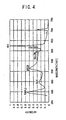
- FIG. 4 is a spectral diagram indicating emission intensity of the white LED according to the first example wherein the purple light excites the respective red/green/blue/yellow phosphors 28 to 31 in the sealant 26, and the respective red/green/blue/yellow phosphors 28 to 31 excited emit the light having the respective blue/green/yellow/red colors as shown in the spectral diagram of emission intensity of FIG. 4 .
- the yellow phosphor 31 is excited with a purple light to emit a yellow light having 560 to 590 nm.
- emission intensity of the respective blue/green/yellow/red colors can be totally elevated as is understood from a comparison of FIG. 4 with FIG. 1 cited in a conventional example. Accordingly, color components of the respective blue/green/yellow/red colors wavelength-converted by the respective red/green/blue/yellow phosphors 28 to 31 become sufficient, so that color rendering properties can be elevated. Furthermore, a conventional average color rendering evaluation number of about 50 to 60 can be improved to about 80 to 90, and in addition, a conventional luminous intensity of about 160 mcd can be elevated to 250 mcd.
- a vicinity of the purple LED 19 may be kept at a high density. In this case, since a lot of lights are wavelength-converted at the vicinity of the purple LED 19, it becomes possible to observe as if a light source is smaller, when the white LED lamp 10 is observed from the outside.
- FIG. 5 is a sectional view showing a white LED lamp according to the second example wherein parts in the second example shown in FIG. 5 corresponding to those of FIG. 2 are designated by the same reference characters as those of FIG. 2 , respectively.
- a white LED lamp 60 shown in FIG. 5 is that of a lens type wherein a purple LED 19 is attached to a metal stem 62 through a mount 21, the metal stem 62 in a form of a cup 17a functioning as a reflecting mirror so as to reflect a light emitted from the purple LED 19 towards the direction over the white LED lamp 60.
- the metal stem 62 is monolithically formed with one 64 of lead frames, one of electrodes of the purple LED 19 on the metal stem 62 is connected with the lead frame 64 through a gold bonding wire 23, and the other electrode is connected with a lead frame 65 through a gold bonding wire 24.
- the inside of the cup 17a is covered with a sealant 26 being a coating material for the sake of fixing the purple LED 19.
- the lead frame 65 and the lead frame 64 formed together with the metal stem 62 are sealed with an external resin 69 being a molding material. Accordingly, the purple LED 19 is doubly sealed with the sealant 26 and the external resin 69.
- the metal stem 62 and the lead frame 64 are also called by the name of a mount lead.
- the interior of the cup 17a is filled with the sealant 26 so as to be held in a lower level than the horizontal surface of the upper edge of the cup 17a.
- Red/green/blue/yellow phosphors 28 to 31 are mixed into the sealant 26.
- the red/green/blue/yellow phosphors 28 to 31 have photoluminescence effects as described in the above first embodiment, so that the light emitted from the purple LED 19 is absorbed to emit a light having a different wavelength from that of the light absorbed.
- Low-melting glass may be used in place of silicone resin or epoxy resin used as the sealant 26.
- Low-melting glass is excellent in resistance to humidity, besides it can prevent invasion of ion harmful to the purple LED 19. Moreover, since low-melting glass can transmit the light emitted from the purple LED 19 without absorbing it, no need of extra light emission with taking an amount of such absorption into consideration.
- a scattering material may be further mixed into the sealant 26 prepared by mixing the red/green/blue/yellow phosphors 28 to 31 into silicone resin, epoxy resin, or low-melting glass.
- the light emitted from the purple LED 19 is reflected diffusely by such scattering material to be a scattered light, so that the light emitted from the purple LED 19 comes easily into conflict with the red/green/blue/yellow phosphors 28 to 31, whereby an amount of a light which is derived from color development of the red/green/blue/yellow phosphors 28 to 31 can be increased.
- Such scattering material is not specifically limited, but well-known materials may be used.
- epoxy resin which becomes transparent after being cured may be employed.
- the purple LED 19 when a voltage is applied across the lead frames 64 and 65, the purple LED 19 emits a light having 395 nm wavelength.
- This purple light excites the respective red/green/blue/yellowphosphors 28 to 31 in the sealant 26, and the phosphors 28 to 31 excited emit lights having the respective colors of blue/green/yellow/red as indicated in the spectral diagram of emission intensity of FIG. 4 .
- the yellow phosphor 31 is excited with a purple light to emit a yellow light having 560 to 590 nm wavelength.
- emission intensity of the respective blue/green/yellow/red colors can be totally elevated as is understood from a comparison of FIG. 4 with FIG. 1 cited in a conventional example. Accordingly, color components of the respective blue/green/yellow/red colors wavelength-converted by the respective phosphors 28 to 31 become sufficient, so that color rendering properties can be elevated. On the other hand, when the red/green/blue/yellow phosphors 28 to 31 are mixed into the external resin 69, the same effects can be obtained.
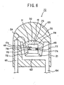
- FIG. 6 is a sectional view showing a white LED lamp according to the third example wherein parts in the third example shown in FIG. 6 corresponding to those of FIG. 5 are designated by the same reference characters as those of FIG. 5 , respectively.
- a white LED lamp 70 shown in FIG. 6 is the one wherein a purple LED 19 can be protected from an overvoltage of static electricity and the like, and the structure thereof is that in which an overvoltage protection device 72 is added to the light source in the white LED lamp 60 shown in FIG. 5 .
- the overvoltage protection device 72 is in a chipped form having the same size as that of the purple LED 19, and it is disposed in between the purple LED 19 and the mount 21.
- the purple LED 19 is flip chip-mounted different from the case of FIG. 5 due to the reason mentioned later.
- the overvoltage protection device 72 is provided with electrodes 74 and 75 for connecting with the purple LED 19 and a lead frame 64.
- the electrode 74 is situated at a position opposed to a p-electrode 48 as shown in FIG. 3 .
- the electrode 75 is situated at a position opposed to an n-electrode 49, and it is connected electrically with a lead frame 65 through a bonding wire 24.
- the electrodes 74 and 75 on the overvoltage protection device 72 are connected to the p-electrode 48 and the n-electrode 49 of the purple LED 19 through gold bumps 74 and 75, respectively.
- a Zener diode which becomes an energization state, when a voltage higher than a previously arranged voltage is applied, a capacitor which absorbs a pulse voltage or the like may be used.
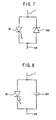
- FIG. 7 is a circuit diagram showing the overvoltage protection device 72 wherein a Zener diode is used.
- the Zener diode 100 as the overvoltage protection device 72 is electrically connected in parallel to the purple LED 19 in which an anode of the purple LED 19 is connected with a cathode of the Zener diode 100, and a cathode of the purple LED 19 is connected with an anode of the Zener diode 100.
- a voltage across terminals of the purple LED 19 is held in the Zener voltage, so that it does not exceed the Zener voltage. Accordingly, it is possible to prevent application of an excessive voltage to the purple LED 19, whereby the purple LED 19 can be protected from an overvoltage, so that destruction of device or appearance of performance degradation can be prevented.
- FIG. 8 is a circuit diagram showing the overvoltage protection device 72 wherein a capacitor is used.
- a capacitor 102 as the overvoltage protection device 72, a chip part for surface-mount may be used.
- the capacitor 102 having such construction as described above is provided with strip-shaped electrodes on the opposite sides thereof, and these electrodes are connected with an anode and a cathode of the purple LED 19 in parallel.
- a charging current flows through the capacitor 102, and it drops instantly a voltage across terminals of the capacitor 102, whereby it is adjusted so as not to increase an applied voltage to the purple LED 19, so that the purple LED 19 can be protected from overvoltage.
- the capacitor 102 functions as a bypass capacitor, so that such extraneous noise can be excluded.
- the purple LED 19 in the white lamp 70 shown in FIG. 6 is flip chip-mounted which is inverted upside-down with respect to the white LED lamp 60 shown in FIG. 5 .
- the reason of which is in that since the overvoltage protection device 72 is provided, electrical connections come to be required for both the overvoltage protection device 72 and the purple LED 19. If the purple LED 19 and the overvoltage protection device 72 are connected through bonding wires, respectively, the number of bonding operations increases, so that its productivity decreases. Besides, since touch and disconnection of bonding wires themselves increase, so that there is a fear of decreasing reliability.
- the purple LED 19 is flip chip-mounted. Namely, the under surface of the sapphire substrate 41 shown in FIG.
- the p-electrode 48 is connected to the electrode 74 of the overvoltage protection device 72 through the gold bump 77, and the n-electrode is connected to the electrode 75 of the overvoltage protection device 72 through the gold bump 78, whereby it is arranged in such that no connection of the bonding wires 23 and 7 to the purple LED 19 is required.
- the transmittive electrode 50 shown in FIG. 3 may be replaced by a non-transmittive electrode.
- n-electrode 49 is thickened so as to have the same height as the surface of the p-electrode 48, or a conductor is newly connected to the n-electrode 42 and the resulting conductor is utilized as an electrode.
- the white LED lamp 70 of the third example constructed as described above when a voltage is applied across the lead frames 64 and 65, lights having respective blue/green/yellow/red colors are emitted as in the case of the white LED lamp 60 shown in FIG. 5 , so that color rendering properties can be elevated as in the case of the white LED lamp 60.
- the overvoltage protection device 72 since the overvoltage protection device 72 is provided, even when an overvoltage due to static electricity and the like is applied, there is not a case where the purple LED 19 is damaged, or a case performance deterioration arises in the purple LED 19. Besides, since the overvoltage protection device 72 functions as a sub-mount, even if the purple LED 19 is flip chip-mounted, a height of bonding positions of the bonding wires 23 and 24 on a chip side does not come down, and as a result, bonding can be made at a position being substantially the same height as that of the case in the white LED lamp 60 shown in FIG. 5 .
- a usual silicon diode may also be used in place of the Zener diode 100.
- a plurality of silicon diodes is connected in series with the same polarities wherein the number of the silicon diodes to be used is determined in such that a value of total forward voltage drop (about 0.7 V x number) corresponds to an operative voltage with respect to overvoltage.
- a variable resister device may also be used for the overvoltage protection device 72. Variable resister device has such a characteristic that a resistance value decreases with increase of an applied voltage, so that it can suppress overvoltage as in the case of the Zener diode 100.
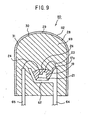
- FIG. 9 is a sectional view showing a white LED lamp according to an embodiment of the present invention wherein parts in the embodiment shown in FIG. 9 corresponding to those of FIG. 5 are designated by the same reference characters as those of FIG. 5 , respectively.
- a white LED lamp 110 shown in FIG. 9 is the one wherein the light emitted from a light emitting element is wavelength-converted to radiate the resulting light outside a resin sealed body of a lens type, and which comprises a structure including lead frames 64 and 65, a metal stem 62, a purple LED 19, a mount 21, bonding wires 23 and 24, a sealant 26 containing no red/green/blue/yellow phosphors 28 to 31, an external resin 69, and a cup 17a, and a further structure including a transmittive fluorescence cover 112 containing the red/green/blue/yellow phosphors 28 to 31 and which adheres to the outer surface of the external resin 69 to envelops the same.
- a resin base material of the fluorescence cover 112 is, for example, transmittive polyester resin, acrylic resin, urethane, nylon, silicone resin, vinyl chloride, polystyrol, Bakelite, CR39 (acryl-glycol-carbonate resin) and the like, and urethane, nylon, and silicone resin are easily put on the external resin 69, because these resins can give elasticity of a certain degree upon the fluorescence cover 112.
- the fluorescence cover 112 has a contour which adheres intimately to the outer surface of the external resin 69, in other words, a shape wherein a hemisphere-shaped cover is formed on the upper part of a cylinder-shaped cover in accordance with one-piece molding, and the resulting fluorescence cover 112 is detachably to the external resin 69.
- the fluorescence cover 112 is to be in a thin film-form to reduce light scattering due to the red/green/blue/yellow phosphors 28 to 31.
- the fluorescence cover 112 is formed into a predetermined shape by injection molding of a resin containing the red/green/blue/yellow phosphors 28 to 31, and then, the resulting fluorescence cover is allowed to adhere intimately to the external resin 69, whereby the operation therefor can be comparatively simply completed.
- the fluorescence cover 112 may be formed in such that a resin raw material containing the red/green/blue/yellow phosphors 28 to 31 is directly sprayed on the external 69 to cure the resin raw material for the sake of forming no air layer between the external resin 69 and the fluorescence cover 112.
- the outgoing light from the purple LED 19 is injected to the fluorescence cover 112 through the sealant 26 and the external resin 69.
- a part of the injected light is absorbed by the red/green/blue/yellow phosphors 28 to 31, and wavelength-converted at the same time to be outgone to the outside.
- a luminous color observed from the outer surface of the fluorescence cover 112 becomes a color obtained by synthesizing these lights, for example, it is white color based on the above-mentioned principle.
- the sealant 26 being a resin sealant body for the purple LED 19 and the external resin 69 do not contain the red/green/blue/yellow phosphors 28 to 31
- the fluorescence cover 112 for covering the outer surface of the external resin 69 contains the red/green/blue/yellow phosphors 28 to 31
- lights having respective colors of blue/green/yellow/red can be emitted as in the case of the white LED lamp 60 shown in FIG. 5 , so that color rendering properties can be similarly elevated.
- the sealant 26 and the external resin 69 do not contain the red/green/blue/yellow phosphors 28 to 31, light scattering due to the red/green/blue/yellow phosphors 28 to 31 does not arise.
- the fluorescence cover 12 is formed into a thin film form, light scattering due to the red/green/blue/yellow phosphors 28 to 31 is comparatively small. Accordingly, when a shape of a lens section of the external resin 69 is formed into an arbitrary shape (a hemisphere-shape in case of the embodiment described above), a desired optical directivity is obtained, whereby deterioration in luminance accompanied with wavelength conversion can be suppressed at the minimum.
- a manner wherein the red/green/blue/yellow phosphors 28 to 31 are applied on the surface of the fluorescence cover 112 can attain the same effects as that of the former manner of containment of the red/green/blue/yellow phosphors 28 to 31.
- the fluorescence cover 112 can put on a commercially available semiconductor light emitting element, so that a white LED lamp can be manufactured inexpensively.
- FIGS. 10(a) and (b) are views each showing a device for a planar light source according to the fourth example of the present invention wherein FIG. 10 (a) is a plan view, and FIG. 10 (b) is a sectional view taken along the line A-A of FIG. 10(a) . It is to be noted that parts in the fourth example shown in FIGS. 10(a) and (b) corresponding to those of FIG. 2 are designated by the same reference characters as those of FIG. 2 , respectively.
- a device 120 for a planar light source shown in FIG. 10 is applied as, for example, a backlight device for a liquid crystal panel.
- the device for a planar light source irradiates a light to a liquid crystal panel from the back side thereof to give brightness or contrast with respect to characters and picture images on the liquid crystal panel being nonluminous, whereby its visual recognition is elevated, and the device for a planar light source comprises the following components.
- the device 120 for a planar light source is composed of a transparent, substantially rectangular light guidance plate 122, a plurality of purple LEDs 19 which are disposed on a side of the light guidance plate 122 in an array-form to be buried therein, whereby they are optically connected with the light guidance plate 122, a light reflection casing 124 for reflecting a light and attached to the light guidance plate 122 so as to surround surfaces except for a light-outgoing surface 122a of the light guidance plate 122, a light scattering pattern 128 obtained by forming a fine and steady concavo-convex pattern on a light reflection surface 126 opposed to the light-outgoing surface 122a of the light guidance plate 122, and a transparent film 130 attached to the light guidance plate 122 so as to cover the light-outgoing surface 122a and containing the red/green/blue/yellow phosphors 28 to 31 inside thereof.
- the respective purple LEDs 19 are attached to the light reflection casing 124 in such that a driving voltage having a predetermined voltage is supplied from a power source through a means for supplying power source such as bonding wires, and lead frames.
- the light scattering pattern 128 functions to scatter the lights emitted from the purple LEDs 19 inside the light guidance plate 22.
- the device 120 for a planar light source constructed as described above, when a driving voltage is applied to the respective purple LEDs 19, lights are outgone from the respective purple LEDs 19 driven.
- the outgoing-lights proceed in the light guidance plate 122 in given directions, they collide against the light scattering pattern 128 formed on the light reflection surface 126 to be outgone from the light-outgoing surface 122a while being reflected and scattering, and they pass through the film 130 as a planar outgoing-light.
- the outgoing-lights of the purple LEDs 19 are partly absorbed by the red/green/blue/yellow phosphors 28 to 31 in the case when they pass through the film 130, and they are wavelength-converted at the same time to be outgone.
- a luminous color observed from the front of the film 130 is a color obtained by synthesizing these lights, for example, it becomes white in accordance with the above-mentioned principle.
- the device 120 for a planar light source of the fourth example since it is constructed in such that the outgoing lights from the purple LEDs 19 are injected to the light guidance plate 122, the lights injected are reflected by the light scattering pattern 128 formed on the light reflection surface 126 of the light guidance plate 122 to outgo the lights from the light-outgoing surface 122a to the film 130 while scattering them, a part of the lights is absorbed by the red/green/blue/yellow phosphors 28 to 31 in the film 130, and at the same time, they are wavelength-converted to be outgone, color rendering properties thereof can be elevated as in the case of the white LED lamp 10 shown in FIG. 2 .
- a structure is the one wherein the red/green/blue/yellow phosphors 28 to 31 are not in directly contact with the purple LEDs 19, deterioration of the red/green/blue/yellow phosphors 28 to 31 can be suppressed for a long period of time, so that a predetermined color tone of such planar light source can be maintained for a long period of time.
- the purple LEDs 19 are optically connected to the light guidance plate 122 by burying the purple LEDs 19 in the light guidance plate 122, the other optical connections such as adhesion bonding of the purple LEDs 19 to end surfaces of the light guidance plate 122, and guidance of a light emitted from the purple LEDs 19 to the end surfaces of the light guidance plate 122 by means of optical conduction means such as optical fiber are also applicable. In this case, a single purple LED 19 may also be applied.
- an LED having a peak wavelength of 400 nm or less is used, so that its emission wavelength exhibits purple color of a low degree of recognition even if it is in visible light ray or ultraviolet ray.
- a color which is sensed by human eyes is a color mixture of lights emitted from LED and phosphor. For this reason, even if an emission wavelength of an LED deviates somewhat towards a long wavelength side, color deviation is hard to appear, because a degree of recognition is low with respect to the light emitted from the LED.
- white color is realized by the use of phosphors of red/green/blue/yellow colors
- such white color may be realized by substituting two types of an alkaline earth metal orthosilicate activated with divalent europium (yellow phosphor) and a blue phosphor for these phosphors. In this case, luminance of a white light emitting device becomes high.
- a light of purple color emitted from a light emitting element is wavelength-converted by phosphors of respective red/green/blue/yellow colors
- a light of yellow component which can be scarcely obtained by such phosphors of respective red/green/blue/yellow colors can be obtained, so that color rendering properties can be elevated.
- a light emitting element having a peak wavelength of 400 nm or less is used, so that its emission wavelength exhibits a purple color of a low degree of recognition even if it is in visible light ray or ultraviolet ray.
- a color which is sensed by human eyes is a color mixture of lights emitted from LED and phosphor. For this reason, even if an emission wavelength of the LED deviates somewhat towards a long wavelength side, color deviation is hard to appear, because a degree of recognition is low with respect to the light emitted from the LED.
Landscapes
- Chemical & Material Sciences (AREA)
- Inorganic Chemistry (AREA)
- Engineering & Computer Science (AREA)
- Materials Engineering (AREA)
- Organic Chemistry (AREA)
- Led Device Packages (AREA)
- Luminescent Compositions (AREA)
- Led Devices (AREA)
Claims (6)
- Dispositif d'émission de lumière blanche, comprenant:un élément (19) d'émission de lumière ayant une longueur d'onde maximale de 400 nm ou moins;un phosphore blanc (31) pour absorber une lumière émise de l'élément (19) d'émission de lumière et pour émettre une lumière avec une longueur d'onde de 560 nm à 590 nm, le phosphore blanc (31) comprenant un silicate de métal alcalino-terreux activé avec de l'europium;un phosphore rouge (28) comprenant du La2O2S: Eu, SM;un phosphore vert (29) comprenant du 3(Ba, Mg, Eu, Mn)O•8Al2O3,un phosphore bleu (30) comprenant du (Sr, Ca, Ba, Eu)10(PO4)6•Cl2, où les phosphores rouge, vert et bleu (28; 29; 30) sont habilités à absorber une lumière émise de l'élément (19) d'émission de lumière et à émettre des lumières rouge, verte, et bleue, respectivement, avec une longueur d'onde différente de celle de la lumière absorbée;un agent d'étanchéité (26) fait d'une résine transparente rendant l'élément (19) d'émission de lumière étanche et une résine externe (69) couvrant l'agent d'étanchéité (26), l'agent d'étanchéité (26) et la résine externe ne comprenant aucun du phosphore blanc (31), du phosphore rouge (28), du phosphore vert (29), et du phosphore bleu (30); etun couvercle (112) à fluorescence transmissive comprenant le phosphore blanc (31), le phosphore rouge (28), le phosphore vert (29), et le phosphore bleu (30),où le couvercle à fluorescence transmissive adhère intimement à la surface externe de la résine externe (69).
- Dispositif d'émission de lumière blanche selon la revendication 1, dans lequel:le phosphore blanc (31) comprend un silicate de potassium de métal alcalino-terreux activé avec un europium divalent représenté par une formule:(2-x-y) SrO· x (Ba, Ca) O· (1-a-b-c-d) SiO2· a P2O5 bAl2O3 cB2O3 dGeO2:y Eu2+où 0 < x < 1,6, 0,005 < y <0,5, 0 < a, b, c, d < 0,5.
- Dispositif d'émission de lumière blanche selon la revendication 1, dans lequel:le phosphore blanc (31) comprend un silicate de potassium de métal alcalino-terreux représenté par une formule:(2-x-y) BaO· x (Sr, Ca) O· (1-a-b-c-d) SiO2· aP2O5 bAl2O3 cB2O3 dGeO2:y Eu2+où 0,01 < x < 1,6, 0,005 < y < 0,5, 0 <a, b, c, d < 0,5.
- Dispositif d'émission de lumière blanche selon la revendication 2 ou 3, dans lequel:dans la formule, au moins l'une des valeurs a, b, c et d est supérieure à 0,01.
- Dispositif d'émission de lumière blanche selon la revendication 1, dans lequel:l'élément (19) d'émission de lumière émet une lumière pourpre avec une longueur d'ondes de 395 nm, l'élément (19) d'émission de lumière est fait d'un semi-conducteur à base de GaN et disposé dans une coupelle (17a) d'un conducteur de montage, où la coupelle est remplie avec l'agent d'étanchéité (26).
- Dispositif d'émission de lumière blanche selon la revendication 5, dans lequel la surface externe de la résine externe (69) est sous forme de lentille.
Applications Claiming Priority (3)
| Application Number | Priority Date | Filing Date | Title |
|---|---|---|---|
| JP2002286089A JP2004127988A (ja) | 2002-09-30 | 2002-09-30 | 白色発光装置 |
| JP2002286089 | 2002-09-30 | ||
| PCT/JP2003/012119 WO2004032251A1 (fr) | 2002-09-30 | 2003-09-22 | Dispositif d'emission de lumiere blanche |
Publications (3)
| Publication Number | Publication Date |
|---|---|
| EP1548850A1 EP1548850A1 (fr) | 2005-06-29 |
| EP1548850A4 EP1548850A4 (fr) | 2005-12-21 |
| EP1548850B1 true EP1548850B1 (fr) | 2010-06-16 |
Family
ID=32063570
Family Applications (1)
| Application Number | Title | Priority Date | Filing Date |
|---|---|---|---|
| EP03799123A Expired - Lifetime EP1548850B1 (fr) | 2002-09-30 | 2003-09-22 | Dispositif d'emission de lumiere blanche |
Country Status (9)
| Country | Link |
|---|---|
| US (1) | US7227190B2 (fr) |
| EP (1) | EP1548850B1 (fr) |
| JP (1) | JP2004127988A (fr) |
| KR (1) | KR100645403B1 (fr) |
| CN (1) | CN100428505C (fr) |
| AT (1) | ATE471575T1 (fr) |
| DE (1) | DE60333025D1 (fr) |
| TW (1) | TWI278125B (fr) |
| WO (1) | WO2004032251A1 (fr) |
Families Citing this family (110)
| Publication number | Priority date | Publication date | Assignee | Title |
|---|---|---|---|---|
| DE10036940A1 (de) * | 2000-07-28 | 2002-02-07 | Patent Treuhand Ges Fuer Elektrische Gluehlampen Mbh | Lumineszenz-Konversions-LED |
| EP1620903B1 (fr) | 2003-04-30 | 2017-08-16 | Cree, Inc. | Blocs de photoemetteurs haute puissance a optiques compactes |
| US7005679B2 (en) | 2003-05-01 | 2006-02-28 | Cree, Inc. | Multiple component solid state white light |
| KR100655894B1 (ko) | 2004-05-06 | 2006-12-08 | 서울옵토디바이스주식회사 | 색온도 및 연색성이 우수한 파장변환 발광장치 |
| KR100658700B1 (ko) | 2004-05-13 | 2006-12-15 | 서울옵토디바이스주식회사 | Rgb 발광소자와 형광체를 조합한 발광장치 |
| JP4747516B2 (ja) * | 2004-06-08 | 2011-08-17 | 富士ゼロックス株式会社 | 垂直共振器型面発光半導体レーザ装置 |
| US7553683B2 (en) * | 2004-06-09 | 2009-06-30 | Philips Lumiled Lighting Co., Llc | Method of forming pre-fabricated wavelength converting elements for semiconductor light emitting devices |
| US8318044B2 (en) | 2004-06-10 | 2012-11-27 | Seoul Semiconductor Co., Ltd. | Light emitting device |
| KR100665299B1 (ko) | 2004-06-10 | 2007-01-04 | 서울반도체 주식회사 | 발광물질 |
| KR100665298B1 (ko) | 2004-06-10 | 2007-01-04 | 서울반도체 주식회사 | 발광장치 |
| US7534633B2 (en) | 2004-07-02 | 2009-05-19 | Cree, Inc. | LED with substrate modifications for enhanced light extraction and method of making same |
| US7575697B2 (en) * | 2004-08-04 | 2009-08-18 | Intematix Corporation | Silicate-based green phosphors |
| JP2006135002A (ja) * | 2004-11-04 | 2006-05-25 | Koito Mfg Co Ltd | 発光デバイス及び車両用灯具 |
| KR100580753B1 (ko) | 2004-12-17 | 2006-05-15 | 엘지이노텍 주식회사 | 발광소자 패키지 |
| KR100663906B1 (ko) * | 2005-03-14 | 2007-01-02 | 서울반도체 주식회사 | 발광 장치 |
| US7385227B2 (en) * | 2005-04-12 | 2008-06-10 | Avago Technologies Ecbu Ip Pte Ltd | Compact light emitting device package with enhanced heat dissipation and method for making the package |
| CN100403563C (zh) * | 2005-04-18 | 2008-07-16 | 光宝科技股份有限公司 | 白光发光二极管元件及相关荧光粉与制备方法 |
| US7754507B2 (en) * | 2005-06-09 | 2010-07-13 | Philips Lumileds Lighting Company, Llc | Method of removing the growth substrate of a semiconductor light emitting device |
| US7736945B2 (en) * | 2005-06-09 | 2010-06-15 | Philips Lumileds Lighting Company, Llc | LED assembly having maximum metal support for laser lift-off of growth substrate |
| KR100638868B1 (ko) * | 2005-06-20 | 2006-10-27 | 삼성전기주식회사 | 금속 반사 층을 형성한 엘이디 패키지 및 그 제조 방법 |
| KR101161383B1 (ko) * | 2005-07-04 | 2012-07-02 | 서울반도체 주식회사 | 발광 다이오드 및 이를 제조하기 위한 방법 |
| DE102005046394A1 (de) * | 2005-09-28 | 2007-04-05 | Taiwan Oasis Technology Co., Ltd. | Weiße Mehrwellenlängen-Leuchtdiode und deren Herstellungsverfahren |
| US7891852B2 (en) * | 2005-10-17 | 2011-02-22 | Koninklijke Philips Electronics Nv | Illumination system using phosphor remote from light source |
| KR101258397B1 (ko) | 2005-11-11 | 2013-04-30 | 서울반도체 주식회사 | 구리 알칼리토 실리케이트 혼성 결정 형광체 |
| US8906262B2 (en) | 2005-12-02 | 2014-12-09 | Lightscape Materials, Inc. | Metal silicate halide phosphors and LED lighting devices using the same |
| KR101055772B1 (ko) | 2005-12-15 | 2011-08-11 | 서울반도체 주식회사 | 발광장치 |
| EP1969633B1 (fr) | 2005-12-22 | 2018-08-29 | Cree, Inc. | Dispositif d' eclairage |
| CN101026152B (zh) * | 2005-12-23 | 2011-04-13 | 财团法人工业技术研究院 | 发光装置 |
| US8030575B2 (en) * | 2005-12-29 | 2011-10-04 | Sensor Electronic Technology, Inc. | Mounting structure providing electrical surge protection |
| WO2007081719A2 (fr) | 2006-01-05 | 2007-07-19 | Illumitex, Inc. | Dispositif optique séparé pour diriger de la lumière depuis une del |
| KR100658970B1 (ko) * | 2006-01-09 | 2006-12-19 | 주식회사 메디아나전자 | 복합 파장의 광을 발생시키는 발광 다이오드 소자 |
| JP4811927B2 (ja) * | 2006-03-23 | 2011-11-09 | ローム株式会社 | Led発光装置およびその製造方法 |
| KR100875443B1 (ko) | 2006-03-31 | 2008-12-23 | 서울반도체 주식회사 | 발광 장치 |
| JP5068472B2 (ja) * | 2006-04-12 | 2012-11-07 | 昭和電工株式会社 | 発光装置の製造方法 |
| EP2011164B1 (fr) * | 2006-04-24 | 2018-08-29 | Cree, Inc. | Del blanche montée en surface vue de côté |
| US8728833B2 (en) * | 2006-05-09 | 2014-05-20 | Intellectual Discovery Co., Ltd. | Light emitting device using a thermally activated coating and method of manufacturing |
| JP4188404B2 (ja) * | 2006-05-19 | 2008-11-26 | 三井金属鉱業株式会社 | 白色蛍光体および白色発光素子乃至装置 |
| KR100755598B1 (ko) * | 2006-06-30 | 2007-09-06 | 삼성전기주식회사 | 질화물 반도체 발광소자 어레이 |
| KR101258227B1 (ko) | 2006-08-29 | 2013-04-25 | 서울반도체 주식회사 | 발광 소자 |
| KR100755612B1 (ko) * | 2006-09-21 | 2007-09-06 | 삼성전기주식회사 | Led 패키지 제조방법 및 백색 광원 모듈 제조방법 |
| KR20090057114A (ko) * | 2006-09-27 | 2009-06-03 | 가부시끼가이샤 도시바 | 반도체 발광 장치, 이 반도체 발광 장치로 이루어진 백라이트 및 표시 장치 |
| US8087960B2 (en) | 2006-10-02 | 2012-01-03 | Illumitex, Inc. | LED system and method |
| KR100862695B1 (ko) * | 2006-10-17 | 2008-10-10 | 삼성전기주식회사 | 백색 발광 다이오드 |
| US7804239B2 (en) | 2006-10-17 | 2010-09-28 | Samsung Led Co., Ltd. | White light emitting diode |
| KR100930171B1 (ko) * | 2006-12-05 | 2009-12-07 | 삼성전기주식회사 | 백색 발광장치 및 이를 이용한 백색 광원 모듈 |
| JP5013596B2 (ja) * | 2007-02-19 | 2012-08-29 | シチズン電子株式会社 | 裏面実装型led |
| US20080197369A1 (en) * | 2007-02-20 | 2008-08-21 | Cree, Inc. | Double flip semiconductor device and method for fabrication |
| US7993038B2 (en) * | 2007-03-06 | 2011-08-09 | Toyoda Gosei Co., Ltd. | Light-emitting device |
| US7781779B2 (en) * | 2007-05-08 | 2010-08-24 | Luminus Devices, Inc. | Light emitting devices including wavelength converting material |
| JP5399617B2 (ja) * | 2007-05-14 | 2014-01-29 | デクセリアルズ株式会社 | 発光組成物及びこれを用いた光源装置並びにこれを用いた表示装置 |
| US8288936B2 (en) * | 2007-06-05 | 2012-10-16 | Sharp Kabushiki Kaisha | Light emitting apparatus, method for manufacturing the light emitting apparatus, electronic device and cell phone device |
| FR2917191B1 (fr) * | 2007-06-11 | 2010-06-11 | Commissariat Energie Atomique | Dispositif d'eclairage pour ecran a cristal liquide |
| WO2008153125A1 (fr) | 2007-06-15 | 2008-12-18 | Sekisui Chemical Co., Ltd. | Agent d'étanchéité pour élément semi-conducteur optique et élément semi-conducteur optique |
| WO2009025469A2 (fr) | 2007-08-22 | 2009-02-26 | Seoul Semiconductor Co., Ltd. | Luminophores en silicate quadratique non stoechiométrique de métaux alcalinoterreux et de cuivre et procédé de préparation de ceux-ci |
| KR101055769B1 (ko) | 2007-08-28 | 2011-08-11 | 서울반도체 주식회사 | 비화학양론적 정방정계 알칼리 토류 실리케이트 형광체를채택한 발광 장치 |
| JP5044329B2 (ja) * | 2007-08-31 | 2012-10-10 | 株式会社東芝 | 発光装置 |
| US7985970B2 (en) | 2009-04-06 | 2011-07-26 | Cree, Inc. | High voltage low current surface-emitting LED |
| JP4613947B2 (ja) * | 2007-12-07 | 2011-01-19 | ソニー株式会社 | 照明装置、色変換素子及び表示装置 |
| US9431589B2 (en) | 2007-12-14 | 2016-08-30 | Cree, Inc. | Textured encapsulant surface in LED packages |
| US20090309114A1 (en) | 2008-01-16 | 2009-12-17 | Luminus Devices, Inc. | Wavelength converting light-emitting devices and methods of making the same |
| JP2011512037A (ja) | 2008-02-08 | 2011-04-14 | イルミテックス, インコーポレイテッド | エミッタ層成形のためのシステムおよび方法 |
| US8242525B2 (en) * | 2008-05-20 | 2012-08-14 | Lightscape Materials, Inc. | Silicate-based phosphors and LED lighting devices using the same |
| KR101438826B1 (ko) * | 2008-06-23 | 2014-09-05 | 엘지이노텍 주식회사 | 발광장치 |
| US8698193B2 (en) * | 2008-07-29 | 2014-04-15 | Sharp Kabushiki Kaisha | Light emitting device and method for manufacturing the same |
| JP5284006B2 (ja) * | 2008-08-25 | 2013-09-11 | シチズン電子株式会社 | 発光装置 |
| KR20100030470A (ko) | 2008-09-10 | 2010-03-18 | 삼성전자주식회사 | 다양한 색 온도의 백색광을 제공할 수 있는 발광 장치 및 발광 시스템 |
| TW201034256A (en) | 2008-12-11 | 2010-09-16 | Illumitex Inc | Systems and methods for packaging light-emitting diode devices |
| JP5651302B2 (ja) * | 2009-02-26 | 2015-01-07 | 株式会社朝日Fr研究所 | 植物栽培用光源 |
| US9093293B2 (en) | 2009-04-06 | 2015-07-28 | Cree, Inc. | High voltage low current surface emitting light emitting diode |
| US8476668B2 (en) * | 2009-04-06 | 2013-07-02 | Cree, Inc. | High voltage low current surface emitting LED |
| JPWO2010150459A1 (ja) * | 2009-06-23 | 2012-12-06 | 株式会社小糸製作所 | 発光モジュール |
| KR101055762B1 (ko) | 2009-09-01 | 2011-08-11 | 서울반도체 주식회사 | 옥시오소실리케이트 발광체를 갖는 발광 물질을 채택한 발광 장치 |
| DE102009030205A1 (de) | 2009-06-24 | 2010-12-30 | Litec-Lp Gmbh | Leuchtstoffe mit Eu(II)-dotierten silikatischen Luminophore |
| JP5226774B2 (ja) * | 2009-07-27 | 2013-07-03 | 株式会社東芝 | 発光装置 |
| KR101301317B1 (ko) * | 2009-08-03 | 2013-08-29 | 엘지디스플레이 주식회사 | 백라이트 유닛 및 이를 이용한 액정표시장치 |
| US8449128B2 (en) | 2009-08-20 | 2013-05-28 | Illumitex, Inc. | System and method for a lens and phosphor layer |
| US8585253B2 (en) | 2009-08-20 | 2013-11-19 | Illumitex, Inc. | System and method for color mixing lens array |
| JP2011066228A (ja) * | 2009-09-17 | 2011-03-31 | Toshiba Corp | 白色led光源、バックライトユニット、液晶パネルおよび液晶tv |
| EP2482351A4 (fr) * | 2009-09-25 | 2013-06-05 | Oceans King Lighting Science | Dispositif électroluminescent semi-conducteur et son procédé d'encapsulation |
| TWI403003B (zh) * | 2009-10-02 | 2013-07-21 | Chi Mei Lighting Tech Corp | 發光二極體及其製造方法 |
| US20130001444A1 (en) * | 2009-12-31 | 2013-01-03 | Mingjie Zhou | White light luminescent device based on purple light leds |
| KR101144754B1 (ko) * | 2010-01-19 | 2012-05-09 | 일진반도체 주식회사 | 백색 발광장치 및 이의 제조방법 |
| JP5820397B2 (ja) * | 2010-01-27 | 2015-11-24 | ヘレウス ノーブルライト アメリカ エルエルシー | マイクロチャンネル冷却型高熱負荷発光装置 |
| JP5535750B2 (ja) | 2010-04-30 | 2014-07-02 | ローム株式会社 | 発光素子モジュール |
| JP5178796B2 (ja) * | 2010-09-10 | 2013-04-10 | 三菱電機株式会社 | 発光装置及び照明装置 |
| JP2012114311A (ja) * | 2010-11-26 | 2012-06-14 | Toshiba Corp | Ledモジュール |
| CN102130236A (zh) * | 2010-12-31 | 2011-07-20 | 北京大学深圳研究生院 | 一种led芯片的封装方法及封装器件 |
| FI122809B (fi) * | 2011-02-15 | 2012-07-13 | Marimils Oy | Valolähde ja valolähdenauha |
| KR101496921B1 (ko) * | 2011-04-05 | 2015-02-27 | 미쓰이 긴조꾸 고교 가부시키가이샤 | 발광 디바이스 |
| JP5863291B2 (ja) * | 2011-06-28 | 2016-02-16 | 株式会社小糸製作所 | 平面発光モジュール |
| WO2013016346A1 (fr) * | 2011-07-25 | 2013-01-31 | Cree, Inc. | Diode électroluminescente émettant par la surface haute tension et faible courant |
| KR20130049568A (ko) * | 2011-11-04 | 2013-05-14 | 삼성전자주식회사 | 반도체 발광소자 및 그 제조방법 |
| TWI455372B (zh) * | 2012-03-07 | 2014-10-01 | Achrolux Inc | Led封裝件及其製法 |
| DE102012007317B4 (de) | 2012-04-12 | 2026-05-07 | Volkswagen Aktiengesellschaft | Vorrichtung zur Befestigung zumindest eines Batteriemoduls in einem Batteriekasten einer Traktionsbatterie |
| CN103375708B (zh) * | 2012-04-26 | 2015-10-28 | 展晶科技(深圳)有限公司 | 发光二极管灯源装置 |
| US9761763B2 (en) * | 2012-12-21 | 2017-09-12 | Soraa, Inc. | Dense-luminescent-materials-coated violet LEDs |
| CN104241262B (zh) | 2013-06-14 | 2020-11-06 | 惠州科锐半导体照明有限公司 | 发光装置以及显示装置 |
| JP6383727B2 (ja) | 2013-08-09 | 2018-08-29 | 株式会社小糸製作所 | 車両用灯具 |
| US10642087B2 (en) | 2014-05-23 | 2020-05-05 | Eyesafe, Llc | Light emission reducing compounds for electronic devices |
| CN104409592A (zh) * | 2014-11-26 | 2015-03-11 | 京东方科技集团股份有限公司 | Led、导光板、背光模组和显示装置 |
| CN105720178B (zh) * | 2016-03-23 | 2018-04-24 | 华灿光电(苏州)有限公司 | 一种发光二极管的封装方法 |
| DE102017108050B4 (de) * | 2017-04-13 | 2022-01-13 | OSRAM Opto Semiconductors Gesellschaft mit beschränkter Haftung | Halbleiterstrahlungsquelle |
| TWI631734B (zh) * | 2017-04-20 | 2018-08-01 | 蔡凱雄 | 發光二極體裝置及其封裝方法 |
| US12321060B1 (en) | 2018-11-28 | 2025-06-03 | Eyesafe Inc. | Color filter enhancements for display devices |
| US11810532B2 (en) | 2018-11-28 | 2023-11-07 | Eyesafe Inc. | Systems for monitoring and regulating harmful blue light exposure from digital devices |
| US11592166B2 (en) | 2020-05-12 | 2023-02-28 | Feit Electric Company, Inc. | Light emitting device having improved illumination and manufacturing flexibility |
| US11876042B2 (en) | 2020-08-03 | 2024-01-16 | Feit Electric Company, Inc. | Omnidirectional flexible light emitting device |
| CN112147667A (zh) * | 2020-09-11 | 2020-12-29 | 兰州空间技术物理研究所 | 一种用于空间低能离子探测的传感器 |
| KR20230153990A (ko) * | 2021-03-10 | 2023-11-07 | 보에 테크놀로지 그룹 컴퍼니 리미티드 | 어레이 기판, 발광 기판 및 디스플레이 장치 |
| CN113937094B (zh) * | 2021-09-14 | 2025-12-05 | 熵基科技股份有限公司 | 图像采集装置、可见光补光结构及其制造方法 |
Family Cites Families (16)
| Publication number | Priority date | Publication date | Assignee | Title |
|---|---|---|---|---|
| TW383508B (en) * | 1996-07-29 | 2000-03-01 | Nichia Kagaku Kogyo Kk | Light emitting device and display |
| JPH1139917A (ja) * | 1997-07-22 | 1999-02-12 | Hewlett Packard Co <Hp> | 高演色性光源 |
| US6252254B1 (en) * | 1998-02-06 | 2001-06-26 | General Electric Company | Light emitting device with phosphor composition |
| JP4306846B2 (ja) * | 1998-11-20 | 2009-08-05 | 株式会社朝日ラバー | 照明装置 |
| US6351069B1 (en) | 1999-02-18 | 2002-02-26 | Lumileds Lighting, U.S., Llc | Red-deficiency-compensating phosphor LED |
| WO2000079605A1 (fr) * | 1999-06-23 | 2000-12-28 | Citizen Electronics Co., Ltd. | Diode électroluminescente |
| WO2001059851A1 (fr) * | 2000-02-09 | 2001-08-16 | Nippon Leiz Corporation | Source lumineuse |
| JP3809760B2 (ja) * | 2000-02-18 | 2006-08-16 | 日亜化学工業株式会社 | 発光ダイオード |
| US6501100B1 (en) | 2000-05-15 | 2002-12-31 | General Electric Company | White light emitting phosphor blend for LED devices |
| JP2001345482A (ja) | 2000-06-01 | 2001-12-14 | Toshiba Corp | 蛍光表示装置 |
| JP2001352101A (ja) | 2000-06-06 | 2001-12-21 | Nichia Chem Ind Ltd | 発光装置 |
| JP2002033520A (ja) * | 2000-07-14 | 2002-01-31 | Toshiba Electronic Engineering Corp | 半導体発光装置 |
| JP2002076445A (ja) * | 2000-09-01 | 2002-03-15 | Sanken Electric Co Ltd | 半導体発光装置 |
| DE10051242A1 (de) | 2000-10-17 | 2002-04-25 | Philips Corp Intellectual Pty | Lichtemittierende Vorrichtung mit beschichtetem Leuchtstoff |
| AT410266B (de) * | 2000-12-28 | 2003-03-25 | Tridonic Optoelectronics Gmbh | Lichtquelle mit einem lichtemittierenden element |
| JP4709405B2 (ja) * | 2001-03-15 | 2011-06-22 | シチズン電子株式会社 | 発光ダイオード |
-
2002
- 2002-09-30 JP JP2002286089A patent/JP2004127988A/ja active Pending
-
2003
- 2003-09-22 WO PCT/JP2003/012119 patent/WO2004032251A1/fr not_active Ceased
- 2003-09-22 EP EP03799123A patent/EP1548850B1/fr not_active Expired - Lifetime
- 2003-09-22 KR KR1020057004392A patent/KR100645403B1/ko not_active Expired - Fee Related
- 2003-09-22 US US10/529,254 patent/US7227190B2/en not_active Expired - Lifetime
- 2003-09-22 DE DE60333025T patent/DE60333025D1/de not_active Expired - Lifetime
- 2003-09-22 CN CNB038214806A patent/CN100428505C/zh not_active Expired - Fee Related
- 2003-09-22 AT AT03799123T patent/ATE471575T1/de active
- 2003-09-26 TW TW092126651A patent/TWI278125B/zh active
Also Published As
| Publication number | Publication date |
|---|---|
| EP1548850A1 (fr) | 2005-06-29 |
| WO2004032251A1 (fr) | 2004-04-15 |
| EP1548850A4 (fr) | 2005-12-21 |
| CN1682381A (zh) | 2005-10-12 |
| KR20050074444A (ko) | 2005-07-18 |
| JP2004127988A (ja) | 2004-04-22 |
| KR100645403B1 (ko) | 2006-11-15 |
| TWI278125B (en) | 2007-04-01 |
| DE60333025D1 (de) | 2010-07-29 |
| ATE471575T1 (de) | 2010-07-15 |
| US20050253158A1 (en) | 2005-11-17 |
| TW200414567A (en) | 2004-08-01 |
| CN100428505C (zh) | 2008-10-22 |
| US7227190B2 (en) | 2007-06-05 |
Similar Documents
| Publication | Publication Date | Title |
|---|---|---|
| EP1548850B1 (fr) | Dispositif d'emission de lumiere blanche | |
| US6943380B2 (en) | Light emitting device having phosphor of alkaline earth metal silicate | |
| JP4124248B2 (ja) | 発光装置 | |
| JP2009117825A (ja) | 白色発光素子 | |
| JPH10228249A (ja) | 発光ダイオード及びそれを用いたled表示装置 | |
| JP3729047B2 (ja) | 発光ダイオード | |
| JP2003124530A (ja) | 発光ダイオード及びそれを用いたled表示装置 | |
| JP2007059667A (ja) | 発光装置 | |
| JP2005244259A (ja) | 発光ダイオード |
Legal Events
| Date | Code | Title | Description |
|---|---|---|---|
| PUAI | Public reference made under article 153(3) epc to a published international application that has entered the european phase |
Free format text: ORIGINAL CODE: 0009012 |
|
| 17P | Request for examination filed |
Effective date: 20050222 |
|
| AK | Designated contracting states |
Kind code of ref document: A1 Designated state(s): AT DE FR GB NL |
|
| A4 | Supplementary search report drawn up and despatched |
Effective date: 20051108 |
|
| RIC1 | Information provided on ipc code assigned before grant |
Ipc: 7C 09K 11/63 B Ipc: 7C 09K 11/64 B Ipc: 7H 01L 33/00 A Ipc: 7C 09K 11/71 B Ipc: 7C 09K 11/59 B Ipc: 7C 09K 11/66 B |
|
| 17Q | First examination report despatched |
Effective date: 20060602 |
|
| GRAP | Despatch of communication of intention to grant a patent |
Free format text: ORIGINAL CODE: EPIDOSNIGR1 |
|
| GRAS | Grant fee paid |
Free format text: ORIGINAL CODE: EPIDOSNIGR3 |
|
| GRAA | (expected) grant |
Free format text: ORIGINAL CODE: 0009210 |
|
| AK | Designated contracting states |
Kind code of ref document: B1 Designated state(s): AT DE FR GB NL |
|
| REF | Corresponds to: |
Ref document number: 60333025 Country of ref document: DE Date of ref document: 20100729 Kind code of ref document: P |
|
| REG | Reference to a national code |
Ref country code: NL Ref legal event code: T3 |
|
| PLBE | No opposition filed within time limit |
Free format text: ORIGINAL CODE: 0009261 |
|
| STAA | Information on the status of an ep patent application or granted ep patent |
Free format text: STATUS: NO OPPOSITION FILED WITHIN TIME LIMIT |
|
| 26N | No opposition filed |
Effective date: 20110317 |
|
| REG | Reference to a national code |
Ref country code: DE Ref legal event code: R097 Ref document number: 60333025 Country of ref document: DE Effective date: 20110316 |
|
| REG | Reference to a national code |
Ref country code: FR Ref legal event code: PLFP Year of fee payment: 14 |
|
| PGFP | Annual fee paid to national office [announced via postgrant information from national office to epo] |
Ref country code: NL Payment date: 20160810 Year of fee payment: 14 |
|
| PGFP | Annual fee paid to national office [announced via postgrant information from national office to epo] |
Ref country code: GB Payment date: 20160921 Year of fee payment: 14 Ref country code: DE Payment date: 20160913 Year of fee payment: 14 |
|
| PGFP | Annual fee paid to national office [announced via postgrant information from national office to epo] |
Ref country code: FR Payment date: 20160816 Year of fee payment: 14 Ref country code: AT Payment date: 20160826 Year of fee payment: 14 |
|
| REG | Reference to a national code |
Ref country code: DE Ref legal event code: R119 Ref document number: 60333025 Country of ref document: DE |
|
| REG | Reference to a national code |
Ref country code: NL Ref legal event code: MM Effective date: 20171001 |
|
| REG | Reference to a national code |
Ref country code: AT Ref legal event code: MM01 Ref document number: 471575 Country of ref document: AT Kind code of ref document: T Effective date: 20170922 |
|
| GBPC | Gb: european patent ceased through non-payment of renewal fee |
Effective date: 20170922 |
|
| PG25 | Lapsed in a contracting state [announced via postgrant information from national office to epo] |
Ref country code: NL Free format text: LAPSE BECAUSE OF NON-PAYMENT OF DUE FEES Effective date: 20171001 |
|
| REG | Reference to a national code |
Ref country code: FR Ref legal event code: ST Effective date: 20180531 |
|
| PG25 | Lapsed in a contracting state [announced via postgrant information from national office to epo] |
Ref country code: GB Free format text: LAPSE BECAUSE OF NON-PAYMENT OF DUE FEES Effective date: 20170922 Ref country code: DE Free format text: LAPSE BECAUSE OF NON-PAYMENT OF DUE FEES Effective date: 20180404 |
|
| PG25 | Lapsed in a contracting state [announced via postgrant information from national office to epo] |
Ref country code: FR Free format text: LAPSE BECAUSE OF NON-PAYMENT OF DUE FEES Effective date: 20171002 Ref country code: AT Free format text: LAPSE BECAUSE OF NON-PAYMENT OF DUE FEES Effective date: 20170922 |