EP1548962B1 - Structure de bus d'atténuation de bruit d'un terminal de communication mobil - Google Patents
Structure de bus d'atténuation de bruit d'un terminal de communication mobil Download PDFInfo
- Publication number
- EP1548962B1 EP1548962B1 EP04030684A EP04030684A EP1548962B1 EP 1548962 B1 EP1548962 B1 EP 1548962B1 EP 04030684 A EP04030684 A EP 04030684A EP 04030684 A EP04030684 A EP 04030684A EP 1548962 B1 EP1548962 B1 EP 1548962B1
- Authority
- EP
- European Patent Office
- Prior art keywords
- bus
- terminal
- memory
- mobile communication
- communication terminal
- Prior art date
- Legal status (The legal status is an assumption and is not a legal conclusion. Google has not performed a legal analysis and makes no representation as to the accuracy of the status listed.)
- Expired - Lifetime
Links
- 238000010295 mobile communication Methods 0.000 title claims abstract description 16
- 230000004044 response Effects 0.000 claims abstract 2
- 239000004973 liquid crystal related substance Substances 0.000 claims description 6
- 230000035945 sensitivity Effects 0.000 description 6
- 238000000034 method Methods 0.000 description 5
- 238000004891 communication Methods 0.000 description 4
- 238000010276 construction Methods 0.000 description 4
- 230000006870 function Effects 0.000 description 2
- 230000003247 decreasing effect Effects 0.000 description 1
- 230000001419 dependent effect Effects 0.000 description 1
- 230000002708 enhancing effect Effects 0.000 description 1
- 229920001690 polydopamine Polymers 0.000 description 1
- 230000001902 propagating effect Effects 0.000 description 1
Images


Classifications
-
- H—ELECTRICITY
- H04—ELECTRIC COMMUNICATION TECHNIQUE
- H04B—TRANSMISSION
- H04B1/00—Details of transmission systems, not covered by a single one of groups H04B3/00 - H04B13/00; Details of transmission systems not characterised by the medium used for transmission
- H04B1/38—Transceivers, i.e. devices in which transmitter and receiver form a structural unit and in which at least one part is used for functions of transmitting and receiving
-
- H—ELECTRICITY
- H04—ELECTRIC COMMUNICATION TECHNIQUE
- H04B—TRANSMISSION
- H04B15/00—Suppression or limitation of noise or interference
- H04B15/02—Reducing interference from electric apparatus by means located at or near the interfering apparatus
Definitions
- the present invention relates to a bus structure and method capable of attenuating digital noise affecting reception sensitivity of a mobile communication terminal.
- a bus structure of a mobile communication terminal connects several elements such as a mobile station modem (MSM), memory, liquid crystal display (LCD), and digital signal processor (DSP).
- MSM mobile station modem
- LCD liquid crystal display
- DSP digital signal processor
- the terminal uses the common bus for addressing memory.
- Fig. 1 illustrates a conventional bus structure of a mobile communication terminal.
- a MSM 1, a memory 2, and a LCD module 5 are connected to a common bus 3, for example a 8-bit or 16-bit bus structure.
- the MSM 1 serves as a master controller for the conventional bus structure.
- the MSM 1 reads data from the memory 2, the LCD module 5, or writes data into the memory 2 by way of the common bus 3. While the MSM 1 is accessing the memory 2 for performing a read or write function, the LCD module is connected to the common bus 3. In another example, while the MSM 1 is accessing the LCD module 5, the memory 2 is connected to the common bus 3. In summary, the memory 2 and the LCD module 5 are continuously connected to the common bus 3. Upon accessing the memory 2 or the LCD module 5, a pulse signal flows into the LCD module 5 or memory 2 generating digital noise.
- the MSM 1 and the memory 2 are separated from RF blocks and positioned at a lower portion 10 of the folder.
- the LCD module 5 is positioned at an upper portion 20 of the folder through a flexible printed circuit board (FPCB).
- the LCD module 5 is connected to the common bus 3.
- the LCD module 5 being farthest from the MSM 1 generates most of the radiated digital noise.
- the conventional terminal having the conventional bus structure has increased digital noise decreasing radio sensitivity of the mobile communication terminal. With increased speed bus processes, digital noise would cause a serious problem to the terminal.
- US 6,052,564 discloses a portable individual calling device such as a pager including a CPU capable of switching between two operation modes, namely low-speed and high-speed.
- the calling device performs a signal-receiving function in an intermittent way.
- the CPU switches from low-speed operation to high-speed operation to process an incoming message transmitted to the calling device.
- the received and processed message Is then stored by the CPU in a RAM memory. After completion of message processing and storage, the CPU returns to low-speed operation and the intermittent receiving operation of calling device is restarted.
- an indication output port of the CPU is shut down to cut off power supply and driving signals for a LCD indicator connected to the output port. In this way, driving of the LCD indicator is suspended for the duration of the high-speed operation of the CPU.
- the document states that CPU noises are thereby prevented from intruding into the inner wiring of the LCD indicator and from there into the radio receiving system of the calling device.
- EP 0 984 362 A1 discloses a bus construction connecting a microprocessor to a phase-lock loop and a plurality of I/O circuits.
- the bus construction includes analog switches to disconnect the phase-lock loop from a common section of the bus construction when data is exchanged between the microprocessor and the I/O circuits.
- the document states that the phase-lock loop can be thereby protected against the bus signals to avoid signal interference in the operation of the circuit.
- WO 03/105360 A1 discloses a folder-type mobile telephone wherein an image processor for decompressing image data is provided in an upper folder part of the phone along with a LCD module and a LCD controller, and a main control section and a program and data memory are housed in a lower folder part of the telephone.
- the present invention conversely, provides a folder-type mobile communication terminal in accordance with claim 1.
- Preferred embodiments are given in the dependent sub-claims.
- the present invention relates to a bus structure and method capable of attenuating digital noise affecting receive sensitivity of a mobile communication terminal.
- the present invention provides a bus structure capable of enhancing radio sensitivity of a mobile communication terminal by reducing radiated digital noise.
- a bus of an LCD module is disconnected from a common bus by using a bus switch, thereby preventing flow of digital noise.
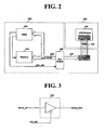
- Fig. 2 illustrates a bus structure of a mobile communication terminal in accordance with a preferred embodiment of the present invention.
- the bus structure provides a bus switch 106 and a bus 107 of an LCD module 105.
- the bus switch 106 connects or disconnects buses of commonly connected elements such the LCD module 105 to a mobile station modem (MSM) 101.
- the bus switch 106 is positioned proximal to a first stage of the bus 107.
- the first bus 107 radiates a large amount of digital noise due to a distal location from a common bus 103.
- the bus switch 106 is positioned at a first stage of an element positioned along an upper portion of the folder unit 120 located farthest from the MSM 101.
- an output control signal (LCD_CS) from the MSM 101 turns-off the bus switch 106 disconnecting the first bus 107 of the LCD module 105 from the common bus 103.
- the bus switch 106 Upon the MSM 101 reading data from the LCD module 105 or writing data to the LCD module 105, the bus switch 106 connects the bus 107 of the LCD module 105 to the common bus 103.
- Fig. 3 illustrates a detailed schematic of the bus switch of Fig. 2 .
- the bus switch 106 is preferably a general integrated logic (IC) for connecting or disconnecting a bus.
- the bus switch 106 in this exemplary example, is a tri-state buffer that is turned on or off in accordance with a control signal (LCD_CS).
- an input terminal of the bus switch 106 is connected to a 16-bit data line and an output terminal is connected to a 16-bit LCD data line.
- the bus switch 106 provides a control terminal for turning on or off the bus switch 106.
- the MSM 101 and the memory 102 exchange data, as shown in Fig. 4 , the MSM 101 outputs a high level control signal (LCD_CS/) turning off the bus switch 106.
- the bus 107 disconnects the LCD module 105 from the common bus 103 which prevents input data (DATA_IN) of the bus switch 106 transmitted to an output terminal.
- the MSM 101 When the MSM 101 writes data to the LCD module 105, the MSM 101 outputs a low level control signal (LCD_CS/) to turn on the bus switch 106.
- the bus 107 of the LCD module 105 is connected to the common bus 103, input data (DATA_IN) may be outputted as output data (DATA_OUT) while the bus switch is in an ON state.
- the bus switch 106 disconnects the bus 107 of the LCD module 105 from the common bus, thus, the bus switch 106 prevents radiated digital noise from the LCD module 105 propagating along the bus structure.
- the present invention provides a bus for a digital signal line of an element positioned along an upper portion of the folder, such as the LCD module.
- the bus disconnects the element from a common bus as necessary to reduce radiated digital noise of the terminal. The reduction in radiated digital noise enhances radio sensitivity of the mobile communication terminal.
- the present invention is described in the context of a mobile terminal, the present invention may also be used in any wired or wireless communication systems using mobile devices, such as PDAs and laptop computers equipped with wired and wireless communication capabilities. Moreover, the use of certain terms to describe the present invention should not limit the scope of the present invention to certain type of wireless communication system, such as UMTS. The present invention is also applicable to other wireless communication systems using different air interfaces and/or physical layers, for example, TDMA, CDMA, FDMA, WCDMA, etc.
Landscapes
- Engineering & Computer Science (AREA)
- Computer Networks & Wireless Communication (AREA)
- Signal Processing (AREA)
- Noise Elimination (AREA)
- Mobile Radio Communication Systems (AREA)
- Transceivers (AREA)
- Telephone Function (AREA)
- Control Of Indicators Other Than Cathode Ray Tubes (AREA)
Claims (3)
- Terminal de communication mobile de type à clapet ayant une partie inférieure (110) et une partie supérieure (120) connectées l'une à l'autre par l'intermédiaire d'une carte de circuit imprimé flexible (104), le terminal comprenant :- une mémoire (102) ayant un premier bus ;- un module d'affichage à cristaux liquides (105) ayant un deuxième bus (107) ;- un bus commun (103) connectant le premier bus et le deuxième bus ;- un modem de station mobile (101) configuré pour échanger des données avec la mémoire (102) et le module d'affichage à cristaux liquides (105) par l'intermédiaire du bus commun (103) ;dans lequel le modem de station mobile (101) et la mémoire (102) sont positionnés sur la partie inférieure (110) du terminal et le module d'affichage à cristaux liquides (105) est positionné sur la partie supérieure (120) du terminal ;
caractérisé par un commutateur de bus (106) positionné sur la partie inférieure (110) du terminal pour déconnecter le deuxième bus (107) du bus commun (103) en réponse à un signal de commande provenant du modem de station mobile (101) lorsque le modem de station mobile lit des données de la mémoire ou écrit des données dans la mémoire. - Terminal selon la revendication 1, dans lequel le commutateur de bus (106) est un tampon trois états.
- Terminal selon la revendication 1 ou 2, dans lequel le commutateur de bus connecte le deuxième bus au bus commun lorsque le modem de station mobile lit des données du module d'affichage à cristaux liquides ou écrit des données dans le module d'affichage à cristaux liquides.
Applications Claiming Priority (2)
| Application Number | Priority Date | Filing Date | Title |
|---|---|---|---|
| KR2003096861 | 2003-12-24 | ||
| KR1020030096861A KR100575758B1 (ko) | 2003-12-24 | 2003-12-24 | 이동통신단말기의 버스구조 |
Publications (3)
| Publication Number | Publication Date |
|---|---|
| EP1548962A2 EP1548962A2 (fr) | 2005-06-29 |
| EP1548962A3 EP1548962A3 (fr) | 2005-08-17 |
| EP1548962B1 true EP1548962B1 (fr) | 2009-05-20 |
Family
ID=34545908
Family Applications (1)
| Application Number | Title | Priority Date | Filing Date |
|---|---|---|---|
| EP04030684A Expired - Lifetime EP1548962B1 (fr) | 2003-12-24 | 2004-12-23 | Structure de bus d'atténuation de bruit d'un terminal de communication mobil |
Country Status (7)
| Country | Link |
|---|---|
| US (1) | US7421530B2 (fr) |
| EP (1) | EP1548962B1 (fr) |
| JP (1) | JP4023812B2 (fr) |
| KR (1) | KR100575758B1 (fr) |
| CN (1) | CN1641615B (fr) |
| AT (1) | ATE431982T1 (fr) |
| DE (1) | DE602004021165D1 (fr) |
Families Citing this family (1)
| Publication number | Priority date | Publication date | Assignee | Title |
|---|---|---|---|---|
| CN106959933B (zh) * | 2017-03-16 | 2019-08-23 | 数据通信科学技术研究所 | 一种总线扩展系统及总线控制的方法 |
Family Cites Families (13)
| Publication number | Priority date | Publication date | Assignee | Title |
|---|---|---|---|---|
| JP2969947B2 (ja) | 1991-03-04 | 1999-11-02 | モトローラ・インコーポレイテッド | データバス・インターフェイス装置 |
| CA2213767A1 (fr) * | 1996-08-20 | 1998-02-20 | Norand Corporation | Systeme de communication sans fil capable de fonctionner en mode de reduction de bruit |
| JPH10257542A (ja) * | 1997-03-13 | 1998-09-25 | Uniden Corp | 携帯型個別呼出装置 |
| US5996039A (en) * | 1997-04-11 | 1999-11-30 | Altera Corporation | Apparatus and method for implementing a tri-state signal driver |
| US6138193A (en) * | 1998-06-23 | 2000-10-24 | Compaq Computer Corporation | System for reducing noise in bus having plurality of first and second set of signals and a delay device for delaying propagation of second signals |
| FI981894A7 (fi) * | 1998-09-04 | 2000-03-05 | Nokia Multimedia Terminals Oy | Väylärakenne |
| US6681125B1 (en) * | 1999-04-08 | 2004-01-20 | Jong-Myung Woo | Wireless telecommunication terminal |
| JP4177525B2 (ja) | 1999-07-23 | 2008-11-05 | 京セラ株式会社 | 携帯電話機 |
| JP2001175606A (ja) | 1999-12-20 | 2001-06-29 | Sony Corp | データ処理装置、データ処理機器およびその方法 |
| JP2002202881A (ja) * | 2000-10-26 | 2002-07-19 | Matsushita Electric Ind Co Ltd | 画像表示装置 |
| JP4349740B2 (ja) | 2000-12-05 | 2009-10-21 | 株式会社ケンウッド | 電子機器 |
| US6907244B2 (en) * | 2000-12-14 | 2005-06-14 | Pulse-Link, Inc. | Hand-off between ultra-wideband cell sites |
| KR100415883B1 (ko) * | 2002-06-08 | 2004-01-24 | 온타임텍 주식회사 | 이미지 프로세서가 상폴더에 구비된 이동통신단말기 |
-
2003
- 2003-12-24 KR KR1020030096861A patent/KR100575758B1/ko not_active Expired - Fee Related
-
2004
- 2004-12-20 JP JP2004368570A patent/JP4023812B2/ja not_active Expired - Fee Related
- 2004-12-23 CN CN2004101032631A patent/CN1641615B/zh not_active Expired - Fee Related
- 2004-12-23 EP EP04030684A patent/EP1548962B1/fr not_active Expired - Lifetime
- 2004-12-23 DE DE602004021165T patent/DE602004021165D1/de not_active Expired - Lifetime
- 2004-12-23 AT AT04030684T patent/ATE431982T1/de not_active IP Right Cessation
- 2004-12-23 US US11/021,228 patent/US7421530B2/en not_active Expired - Fee Related
Also Published As
| Publication number | Publication date |
|---|---|
| US7421530B2 (en) | 2008-09-02 |
| EP1548962A3 (fr) | 2005-08-17 |
| KR100575758B1 (ko) | 2006-05-03 |
| CN1641615B (zh) | 2010-05-05 |
| JP4023812B2 (ja) | 2007-12-19 |
| JP2005192215A (ja) | 2005-07-14 |
| EP1548962A2 (fr) | 2005-06-29 |
| ATE431982T1 (de) | 2009-06-15 |
| CN1641615A (zh) | 2005-07-20 |
| DE602004021165D1 (de) | 2009-07-02 |
| US20050144350A1 (en) | 2005-06-30 |
| KR20050065097A (ko) | 2005-06-29 |
Similar Documents
| Publication | Publication Date | Title |
|---|---|---|
| JP2718399B2 (ja) | コンピュータ接続対応データ無線機 | |
| JP3813849B2 (ja) | カード装置 | |
| EP1394724B1 (fr) | Méthode et système de reconnaissance de caractères pour un terminal mobile de communication | |
| EP1356366B1 (fr) | Dispositif peripherique d'ordinateur exploitable meme en cas de suspension du fonctionnement du processeur central | |
| US6754509B1 (en) | Mobile communication device having dual micro processor architecture with shared digital signal processor and shared memory | |
| US20020144166A1 (en) | Motherboard with reduced power consumption | |
| US9322923B2 (en) | Method of switching electronic apparatus between different modes according to connection status of wireless connection and electronic apparatus thereof | |
| KR0157129B1 (ko) | 확장장치와 휴대용 컴퓨터간의 신호 연결 제어장치 및 이를 포함한 확장장치 | |
| US6938178B2 (en) | Terminal device and real-time clock control method therefor enabling preservation of clock/calendar information and high information readout speed | |
| EP0849683B1 (fr) | Carte d'extension, interface de carte et dispositif électronique | |
| US7953898B2 (en) | Apparatus and method for using expansion key in portable terminal | |
| US7717350B2 (en) | Portable computing platform having multiple operating modes and heterogeneous processors | |
| EP1548962B1 (fr) | Structure de bus d'atténuation de bruit d'un terminal de communication mobil | |
| JP2005123961A (ja) | 情報機器装置 | |
| US20050278469A1 (en) | Computer system and control method of the same | |
| US20040003145A1 (en) | Method and apparatus to transfer information | |
| US20040233772A1 (en) | Semiconductor device, semiconductor circuit, electronic equipment, and method of controlling clock-supply | |
| KR100318849B1 (ko) | Cdma 이동통신 시스템에서의 cpu 및 dsp간인터페이스 장치 | |
| CN100371980C (zh) | 显示控制装置 | |
| KR100452844B1 (ko) | 절전기능을 갖는 휴대용 단말기 및 그 제어방법 | |
| CN1282188A (zh) | 移动电话机 | |
| US20040240307A1 (en) | Semiconductor device, semiconductor circuit, electronic equipment, and method of controlling clock-supply | |
| KR100506226B1 (ko) | 디지털 이동 통신 단말기에서 터치패널 및 표시장치인터페이스 장치 | |
| JP4364211B2 (ja) | カード装置 | |
| MXPA04003339A (es) | Multiplexor de puerto de interfase multiple. |
Legal Events
| Date | Code | Title | Description |
|---|---|---|---|
| PUAI | Public reference made under article 153(3) epc to a published international application that has entered the european phase |
Free format text: ORIGINAL CODE: 0009012 |
|
| 17P | Request for examination filed |
Effective date: 20041223 |
|
| AK | Designated contracting states |
Kind code of ref document: A2 Designated state(s): AT BE BG CH CY CZ DE DK EE ES FI FR GB GR HU IE IS IT LI LT LU MC NL PL PT RO SE SI SK TR |
|
| AX | Request for extension of the european patent |
Extension state: AL BA HR LV MK YU |
|
| PUAL | Search report despatched |
Free format text: ORIGINAL CODE: 0009013 |
|
| RIN1 | Information on inventor provided before grant (corrected) |
Inventor name: CHOI, SANG-HUN |
|
| AK | Designated contracting states |
Kind code of ref document: A3 Designated state(s): AT BE BG CH CY CZ DE DK EE ES FI FR GB GR HU IE IS IT LI LT LU MC NL PL PT RO SE SI SK TR |
|
| AX | Request for extension of the european patent |
Extension state: AL BA HR LV MK YU |
|
| RIC1 | Information provided on ipc code assigned before grant |
Ipc: 7H 04B 15/00 A Ipc: 7G 06F 13/40 B |
|
| AKX | Designation fees paid |
Designated state(s): AT BE BG CH CY CZ DE DK EE ES FI FR GB GR HU IE IS IT LI LT LU MC NL PL PT RO SE SI SK TR |
|
| 17Q | First examination report despatched |
Effective date: 20070803 |
|
| GRAP | Despatch of communication of intention to grant a patent |
Free format text: ORIGINAL CODE: EPIDOSNIGR1 |
|
| GRAS | Grant fee paid |
Free format text: ORIGINAL CODE: EPIDOSNIGR3 |
|
| GRAA | (expected) grant |
Free format text: ORIGINAL CODE: 0009210 |
|
| RAP1 | Party data changed (applicant data changed or rights of an application transferred) |
Owner name: LG ELECTRONICS INC. |
|
| AK | Designated contracting states |
Kind code of ref document: B1 Designated state(s): AT BE BG CH CY CZ DE DK EE ES FI FR GB GR HU IE IS IT LI LT LU MC NL PL PT RO SE SI SK TR |
|
| REG | Reference to a national code |
Ref country code: GB Ref legal event code: FG4D |
|
| REG | Reference to a national code |
Ref country code: CH Ref legal event code: EP |
|
| REG | Reference to a national code |
Ref country code: IE Ref legal event code: FG4D |
|
| REF | Corresponds to: |
Ref document number: 602004021165 Country of ref document: DE Date of ref document: 20090702 Kind code of ref document: P |
|
| PG25 | Lapsed in a contracting state [announced via postgrant information from national office to epo] |
Ref country code: LT Free format text: LAPSE BECAUSE OF FAILURE TO SUBMIT A TRANSLATION OF THE DESCRIPTION OR TO PAY THE FEE WITHIN THE PRESCRIBED TIME-LIMIT Effective date: 20090520 Ref country code: ES Free format text: LAPSE BECAUSE OF FAILURE TO SUBMIT A TRANSLATION OF THE DESCRIPTION OR TO PAY THE FEE WITHIN THE PRESCRIBED TIME-LIMIT Effective date: 20090831 Ref country code: AT Free format text: LAPSE BECAUSE OF FAILURE TO SUBMIT A TRANSLATION OF THE DESCRIPTION OR TO PAY THE FEE WITHIN THE PRESCRIBED TIME-LIMIT Effective date: 20090520 Ref country code: FI Free format text: LAPSE BECAUSE OF FAILURE TO SUBMIT A TRANSLATION OF THE DESCRIPTION OR TO PAY THE FEE WITHIN THE PRESCRIBED TIME-LIMIT Effective date: 20090520 Ref country code: PT Free format text: LAPSE BECAUSE OF FAILURE TO SUBMIT A TRANSLATION OF THE DESCRIPTION OR TO PAY THE FEE WITHIN THE PRESCRIBED TIME-LIMIT Effective date: 20090920 |
|
| NLV1 | Nl: lapsed or annulled due to failure to fulfill the requirements of art. 29p and 29m of the patents act | ||
| PG25 | Lapsed in a contracting state [announced via postgrant information from national office to epo] |
Ref country code: NL Free format text: LAPSE BECAUSE OF FAILURE TO SUBMIT A TRANSLATION OF THE DESCRIPTION OR TO PAY THE FEE WITHIN THE PRESCRIBED TIME-LIMIT Effective date: 20090520 Ref country code: IS Free format text: LAPSE BECAUSE OF FAILURE TO SUBMIT A TRANSLATION OF THE DESCRIPTION OR TO PAY THE FEE WITHIN THE PRESCRIBED TIME-LIMIT Effective date: 20090920 Ref country code: SE Free format text: LAPSE BECAUSE OF FAILURE TO SUBMIT A TRANSLATION OF THE DESCRIPTION OR TO PAY THE FEE WITHIN THE PRESCRIBED TIME-LIMIT Effective date: 20090820 Ref country code: PL Free format text: LAPSE BECAUSE OF FAILURE TO SUBMIT A TRANSLATION OF THE DESCRIPTION OR TO PAY THE FEE WITHIN THE PRESCRIBED TIME-LIMIT Effective date: 20090520 Ref country code: SI Free format text: LAPSE BECAUSE OF FAILURE TO SUBMIT A TRANSLATION OF THE DESCRIPTION OR TO PAY THE FEE WITHIN THE PRESCRIBED TIME-LIMIT Effective date: 20090520 |
|
| PG25 | Lapsed in a contracting state [announced via postgrant information from national office to epo] |
Ref country code: DK Free format text: LAPSE BECAUSE OF FAILURE TO SUBMIT A TRANSLATION OF THE DESCRIPTION OR TO PAY THE FEE WITHIN THE PRESCRIBED TIME-LIMIT Effective date: 20090520 Ref country code: CZ Free format text: LAPSE BECAUSE OF FAILURE TO SUBMIT A TRANSLATION OF THE DESCRIPTION OR TO PAY THE FEE WITHIN THE PRESCRIBED TIME-LIMIT Effective date: 20090520 Ref country code: EE Free format text: LAPSE BECAUSE OF FAILURE TO SUBMIT A TRANSLATION OF THE DESCRIPTION OR TO PAY THE FEE WITHIN THE PRESCRIBED TIME-LIMIT Effective date: 20090520 Ref country code: RO Free format text: LAPSE BECAUSE OF FAILURE TO SUBMIT A TRANSLATION OF THE DESCRIPTION OR TO PAY THE FEE WITHIN THE PRESCRIBED TIME-LIMIT Effective date: 20090520 |
|
| PG25 | Lapsed in a contracting state [announced via postgrant information from national office to epo] |
Ref country code: SK Free format text: LAPSE BECAUSE OF FAILURE TO SUBMIT A TRANSLATION OF THE DESCRIPTION OR TO PAY THE FEE WITHIN THE PRESCRIBED TIME-LIMIT Effective date: 20090520 Ref country code: BE Free format text: LAPSE BECAUSE OF FAILURE TO SUBMIT A TRANSLATION OF THE DESCRIPTION OR TO PAY THE FEE WITHIN THE PRESCRIBED TIME-LIMIT Effective date: 20090520 |
|
| PLBE | No opposition filed within time limit |
Free format text: ORIGINAL CODE: 0009261 |
|
| STAA | Information on the status of an ep patent application or granted ep patent |
Free format text: STATUS: NO OPPOSITION FILED WITHIN TIME LIMIT |
|
| PG25 | Lapsed in a contracting state [announced via postgrant information from national office to epo] |
Ref country code: BG Free format text: LAPSE BECAUSE OF FAILURE TO SUBMIT A TRANSLATION OF THE DESCRIPTION OR TO PAY THE FEE WITHIN THE PRESCRIBED TIME-LIMIT Effective date: 20090820 |
|
| 26N | No opposition filed |
Effective date: 20100223 |
|
| PG25 | Lapsed in a contracting state [announced via postgrant information from national office to epo] |
Ref country code: MC Free format text: LAPSE BECAUSE OF NON-PAYMENT OF DUE FEES Effective date: 20100701 |
|
| REG | Reference to a national code |
Ref country code: CH Ref legal event code: PL |
|
| PG25 | Lapsed in a contracting state [announced via postgrant information from national office to epo] |
Ref country code: CH Free format text: LAPSE BECAUSE OF NON-PAYMENT OF DUE FEES Effective date: 20091231 Ref country code: GR Free format text: LAPSE BECAUSE OF FAILURE TO SUBMIT A TRANSLATION OF THE DESCRIPTION OR TO PAY THE FEE WITHIN THE PRESCRIBED TIME-LIMIT Effective date: 20090821 Ref country code: IE Free format text: LAPSE BECAUSE OF NON-PAYMENT OF DUE FEES Effective date: 20091223 Ref country code: LI Free format text: LAPSE BECAUSE OF NON-PAYMENT OF DUE FEES Effective date: 20091231 |
|
| PG25 | Lapsed in a contracting state [announced via postgrant information from national office to epo] |
Ref country code: LU Free format text: LAPSE BECAUSE OF NON-PAYMENT OF DUE FEES Effective date: 20091223 |
|
| PG25 | Lapsed in a contracting state [announced via postgrant information from national office to epo] |
Ref country code: HU Free format text: LAPSE BECAUSE OF FAILURE TO SUBMIT A TRANSLATION OF THE DESCRIPTION OR TO PAY THE FEE WITHIN THE PRESCRIBED TIME-LIMIT Effective date: 20091121 |
|
| PG25 | Lapsed in a contracting state [announced via postgrant information from national office to epo] |
Ref country code: TR Free format text: LAPSE BECAUSE OF FAILURE TO SUBMIT A TRANSLATION OF THE DESCRIPTION OR TO PAY THE FEE WITHIN THE PRESCRIBED TIME-LIMIT Effective date: 20090520 |
|
| PG25 | Lapsed in a contracting state [announced via postgrant information from national office to epo] |
Ref country code: CY Free format text: LAPSE BECAUSE OF FAILURE TO SUBMIT A TRANSLATION OF THE DESCRIPTION OR TO PAY THE FEE WITHIN THE PRESCRIBED TIME-LIMIT Effective date: 20090520 |
|
| PGFP | Annual fee paid to national office [announced via postgrant information from national office to epo] |
Ref country code: GB Payment date: 20131112 Year of fee payment: 10 |
|
| GBPC | Gb: european patent ceased through non-payment of renewal fee |
Effective date: 20141223 |
|
| PG25 | Lapsed in a contracting state [announced via postgrant information from national office to epo] |
Ref country code: GB Free format text: LAPSE BECAUSE OF NON-PAYMENT OF DUE FEES Effective date: 20141223 |
|
| REG | Reference to a national code |
Ref country code: FR Ref legal event code: PLFP Year of fee payment: 12 |
|
| PGFP | Annual fee paid to national office [announced via postgrant information from national office to epo] |
Ref country code: DE Payment date: 20151111 Year of fee payment: 12 Ref country code: IT Payment date: 20151215 Year of fee payment: 12 |
|
| PGFP | Annual fee paid to national office [announced via postgrant information from national office to epo] |
Ref country code: FR Payment date: 20151113 Year of fee payment: 12 |
|
| REG | Reference to a national code |
Ref country code: DE Ref legal event code: R119 Ref document number: 602004021165 Country of ref document: DE |
|
| REG | Reference to a national code |
Ref country code: FR Ref legal event code: ST Effective date: 20170831 |
|
| PG25 | Lapsed in a contracting state [announced via postgrant information from national office to epo] |
Ref country code: FR Free format text: LAPSE BECAUSE OF NON-PAYMENT OF DUE FEES Effective date: 20170102 Ref country code: IT Free format text: LAPSE BECAUSE OF NON-PAYMENT OF DUE FEES Effective date: 20161223 |
|
| PG25 | Lapsed in a contracting state [announced via postgrant information from national office to epo] |
Ref country code: DE Free format text: LAPSE BECAUSE OF NON-PAYMENT OF DUE FEES Effective date: 20170701 |