EP1550194B1 - Schutzeinrichtung zur verhinderung des flusses unerwünschter transienten des differenzmodus - Google Patents
Schutzeinrichtung zur verhinderung des flusses unerwünschter transienten des differenzmodus Download PDFInfo
- Publication number
- EP1550194B1 EP1550194B1 EP03747722A EP03747722A EP1550194B1 EP 1550194 B1 EP1550194 B1 EP 1550194B1 EP 03747722 A EP03747722 A EP 03747722A EP 03747722 A EP03747722 A EP 03747722A EP 1550194 B1 EP1550194 B1 EP 1550194B1
- Authority
- EP
- European Patent Office
- Prior art keywords
- connection point
- protection
- solid state
- cable
- output connection
- Prior art date
- Legal status (The legal status is an assumption and is not a legal conclusion. Google has not performed a legal analysis and makes no representation as to the accuracy of the status listed.)
- Expired - Lifetime
Links
- 238000002955 isolation Methods 0.000 claims description 27
- 230000015556 catabolic process Effects 0.000 claims description 10
- 239000007787 solid Substances 0.000 claims description 10
- 230000001052 transient effect Effects 0.000 claims description 8
- 230000001960 triggered effect Effects 0.000 claims description 3
- 230000000903 blocking effect Effects 0.000 claims description 2
- 239000013589 supplement Substances 0.000 claims 1
- 238000010586 diagram Methods 0.000 description 14
- 230000001012 protector Effects 0.000 description 5
- 239000004020 conductor Substances 0.000 description 3
- 230000008878 coupling Effects 0.000 description 3
- 238000010168 coupling process Methods 0.000 description 3
- 238000005859 coupling reaction Methods 0.000 description 3
- 238000000034 method Methods 0.000 description 3
- 230000001939 inductive effect Effects 0.000 description 2
- 230000005540 biological transmission Effects 0.000 description 1
- 230000000694 effects Effects 0.000 description 1
- 230000036039 immunity Effects 0.000 description 1
- 238000003780 insertion Methods 0.000 description 1
- 230000037431 insertion Effects 0.000 description 1
- 230000007257 malfunction Effects 0.000 description 1
- 238000012986 modification Methods 0.000 description 1
- 230000004048 modification Effects 0.000 description 1
Images




Classifications
-
- H—ELECTRICITY
- H04—ELECTRIC COMMUNICATION TECHNIQUE
- H04M—TELEPHONIC COMMUNICATION
- H04M3/00—Automatic or semi-automatic exchanges
- H04M3/18—Automatic or semi-automatic exchanges with means for reducing interference or noise; with means for reducing effects due to line faults with means for protecting lines
-
- H—ELECTRICITY
- H02—GENERATION; CONVERSION OR DISTRIBUTION OF ELECTRIC POWER
- H02H—EMERGENCY PROTECTIVE CIRCUIT ARRANGEMENTS
- H02H9/00—Emergency protective circuit arrangements for limiting excess current or voltage without disconnection
- H02H9/02—Emergency protective circuit arrangements for limiting excess current or voltage without disconnection responsive to excess current
- H02H9/025—Current limitation using field effect transistors
-
- H—ELECTRICITY
- H02—GENERATION; CONVERSION OR DISTRIBUTION OF ELECTRIC POWER
- H02H—EMERGENCY PROTECTIVE CIRCUIT ARRANGEMENTS
- H02H9/00—Emergency protective circuit arrangements for limiting excess current or voltage without disconnection
- H02H9/005—Emergency protective circuit arrangements for limiting excess current or voltage without disconnection avoiding undesired transient conditions
-
- H—ELECTRICITY
- H02—GENERATION; CONVERSION OR DISTRIBUTION OF ELECTRIC POWER
- H02H—EMERGENCY PROTECTIVE CIRCUIT ARRANGEMENTS
- H02H9/00—Emergency protective circuit arrangements for limiting excess current or voltage without disconnection
- H02H9/04—Emergency protective circuit arrangements for limiting excess current or voltage without disconnection responsive to excess voltage
- H02H9/06—Emergency protective circuit arrangements for limiting excess current or voltage without disconnection responsive to excess voltage using spark-gap arresters
Definitions
- the present invention relates to electrical surge protection devices.
- Figure 1 is a schematic diagram of a typical arrangement whereby a cable including a pair of conductors 2, 4 terminate on an isolation transformer 6 which is connected to a load 12.
- the potential on both conductors 2 and 4 will vary virtually identically thereby causing substantially zero net current to flow through the primary coil 8 of transformer 6.
- the common mode transient does not induce a fault current in secondary coil 10 and so isolation transformer 6 provides common mode protection to load 12.
- LANs local area computer data networks
- a digital processing card in the form of a network interface card (NIC), or as it is often called a "LAN card” couples to J8-45 plug 22 of LAN cable 16 by means of J8-45 socket 18.
- LAN card 14 includes an isolation transformer module 20 that couples socket 18 to a data processing chip 24 which in turn communicates with the central processor 26 of a workstation by means of PCI slot connectors 28 that are received into a PCI connector 30 which is in turn mounted on a mainboard 32 of the workstation.
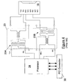
- Figure 4 is a schematic diagram of the prior art card of Figure 3 wherein like indicia are used to refer to like components.
- the card receives and transmits data pulses by means of respective balanced twisted pair wires that are enclosed in LAN cable 16 and which terminate on the RX+ and RX- pins and TX+ and TX- pins of J8-45 socket 18.
- Isolation module 20 includes a pair of transformers 20A and 20B which respectively provide isolation for processing chip 24 from transients on the transmit and receive twisted pairs.
- isolation transformers 20A and 20B provide considerable immunity from damaging common mode transients but not from differential mode transients. For example, in the event of a voltage transient occurring at the RX+ pin but not on the RX- pin then that transient will be transmitted across the isolation transformer and may damage processing chip 24.
- Document US 6 178 080 discloses a device having two connected in parallel unipolar solid state protection devices.
- Document US 4 996 706 discloses on apparatus comprising serially connected a transformer and two surge protector units. It is an object of the present invention to provide a convenient means for addressing the problems posed by differential mode transients as discussed above.
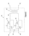
- Isolation module 34 includes a common mode isolation device 42 which in the present embodiment comprises a transformer although it will be realised that it could instead be some other common mode isolation device such as an opto-isolator.
- Isolation module 34 includes two identical series connected unipolar transient blocking units (TBUs) 36 and 38 connected at respective sides of primary coil 40 of transformer 42.
- TBUs unipolar transient blocking units
- a TBU is a transistor device configured to open-circuit once the current through it reaches a certain predetermined trigger level.
- TBU 36 consists of two depletion mode FETs being N-channel FET Q1 and P-channel FET Q2.
- Q1 and Q2 are connected with their conduction paths in series.
- the gate electrode of transistor Q1 is coupled to the drain electrode of transistor Q2.
- the source electrodes of Q1 and Q2 are coupled to each other and the drain electrode of transistor Q1 is coupled to a first terminal 44.
- Resistor R1 extends between the drain electrode of Q1 and the gate electrode of Q2.
- the drain of Q2 is connected to a first side of primary coil 40.
- TBU 36 functions as a fuse for positive current flowing from terminal 44 through to the primary coil.
- TBU 38 The structure of TBU 38 is identical to that of TBU 36 so that TBU 38 acts as a fuse for positive current flowing from terminal 46 towards primary coil 40.
- TBU 38 and TBU 36 are selected so that they have as close as possible insertion loss in order that the balance of the circuit is maintained.
- TBUs 36 and 38 protect a load connected across terminals 43 and 45 from differential surge currents by triggering to an open circuit when the current through the load reaches the preset trigger level. If the differential current into terminal 44 attains the trigger level then TBU 36 will open-circuit. Alternatively if the differential current flowing out of terminal 44 attains the trigger level then TBU 38 will trigger. Of course, the TBUs could be reverse-orientated relative to the configuration depicted in Figure 4 . In that case if the differential current into terminal 44 attains the trigger level then TBU 38 would open circuit and conversely if the differential current flowing out of terminal 44 attained the trigger level then TBU 36 would trigger.
- surge arrestor 48 may be included.
- a gas arrestor, as depicted at item 48 is typically used. However, any suitable surge arrestor could be used as an alternative.
- Surge arrestor 48 is connected line-to-line across terminals 44 and 46 and is selected so that it will trigger at 90% of the TBUs' breakdown voltage.
- the surge arrestor will trigger and short the surge before it can cause breakdown of the triggered TBU and subsequently be transmitted across isolation transformer 42 to potentially damage any load connected between output terminals 43 and 45.
- Suitable TBU's may be purchased from Fultec Pty Ltd of,Building 76A, University of Queensland Campus, St Lucia, Brisbane, Queensland, Australia. Circuits for implementing suitable TBUs are described in granted United States patent No. 5,742,463 and in international patent application No. PCT/AU03/00175 , both by the present inventor. The descriptions of both US 5,742,463 and PCT/AU03/00175 are hereby both incorporated in their entireties by cross-reference.
- a differential mode protection device 43 is conveniently provided in a single package having four connectors A, B, C, D as shown.
- the device may be provided with or without a surge arrestor as desired.
- a schematic diagram of the internal circuit of device 43 without surge arrestor is shown in Figure 7 whereas a schematic for a further version with surge arrestor is shown in Figure 8 .
- Further variations of the device are possible. For example an eight terminal version of the device might be provided including two of the circuits of Figure 7 or Figure 8 .
- FIG. 9 A schematic diagram of a digital processing card, in the present example a LAN card, according to a preferred embodiment of the invention is shown in Figure 9 . It will be noted that the LAN card of Figure 9 incorporates two pairs of TBUs 51A, 51B and 52A, 52B placed in series with the TX+, TX-, and RX+, RX- terminals of socket 18 respectively.
- the TBUs are each identical to TBUs 36 and 38 of Figure 5 and might be provided in an eight terminal version of device 43 of Figure 6 .
- Surge arrestors 19 and 21 are connected across the TX+, TX- and RX+, RX- pins respectively. The surge arrestors are selected so that they will trigger at 90% of the TBUs' breakdown voltage. As previously explained, in the event of a differential mode surge approaching the breakdown voltage of the TBUs the surge arrestors will trigger and short the surge before it can cause breakdown of the TBUs and subsequently be transmitted across isolation transformer to potentially damage logic circuitry 24.
- FIG 10 depicts the external appearance of a differential mode surge protector 50 according to a further embodiment of the present invention while Figure 11 is a corresponding schematic diagram.
- Surge protector 50 includes a J8-45 plug 52 for connection to a socket of a LAN card.
- the J8-45 plug is coupled to a differential mode protection module 54 which includes TBU's and surge arrestors as shown in Figure 11 .
- the surge protector further includes a J8-45 socket 58 which is coupled to circuitry in module 54 and which is intended to receive a LAN cable.
- Figure 12 is a variation of the differential mode surge protector of Figures 10 and 11 being a cable 63 incorporating differential mode protection according to the present invention.
- Cable 63 includes a connector 52 for connection to a digital processing card.
- a differential mode protection module 54 identical to the one in Figure 10 and containing the circuitry depicted in Figure 11 is coupled to connector 52.
- a relatively long run of cable 61 connects protection module 54, which includes TBU's and surge arrestors as shown in Figure 11 , to remote connector 59.
- connector 52 be plugged into a digital processing card such as a LAN card whereas connector 59 is plugged into a remote device such as a network hub.
- a second module may be incorporated proximal to plug 59.
- the cable shown in Figure 12 are of course possible.
- the circuitry that is provided inside housing 54 might be integrated into one or the other of connectors 52 and 59.
Landscapes
- Engineering & Computer Science (AREA)
- Power Engineering (AREA)
- Signal Processing (AREA)
- Emergency Protection Circuit Devices (AREA)
- Protection Of Static Devices (AREA)
Claims (12)
- Überspannungsschutzvorrichtung, die folgendes aufweist:einen ersten Eingangs-Anschlusspunkt (A) und einen entsprechenden ersten Ausgangs-Anschlusspunkt (C);einen zweiten Eingangs-Anschlusspunkt (B) und einen entsprechenden zweiten Ausgangs-Anschlusspunkt (D);eine erste unipolare Festkörper-Schutzvorrichtung (36), wobei die genannte erste Schutzvorrichtung (36) in Reihe geschaltet zwischen dem genannten ersten Eingangs-Anschlusspunkt (A) und dem genannten ersten Ausgangs-Anschlusspunkt (C) angeordnet ist, wobei die genannte erste unipolare Festkörper-Schutzvorrichtung (36) so angeordnet ist, dass sie so funktionsfähig ist, dass sie den elektrischen Strom nur in eine Richtung von dem genannten ersten Eingangs-Anschlusspunkt (A) zu dem genannten ersten Ausgangs-Anschlusspunkt (C) begrenzt;eine zweite unipolare Festkörper-Schutzvorrichtung (38), wobei die genannte zweite Schutzvorrichtung (38) in Reihe geschaltet zwischen dem genannten zweiten Eingangs-Anschlusspunkt (B) und dem genannten zweiten Ausgangs-Anschlusspunkt (D) angeordnet ist, wobei die beiden genannten unipolaren Festkörper-Schutzvorrichtungen (36, 38) so ausgerichtet sind, dass sie den Strom in die gleiche Richtung im Verhältnis zu den genannten Eingangs- und den genannten Ausgangs-Anschlusspunkten begrenzen; unddadurch gekennzeichnet, dass die Überspannungsschutzvorrichtung folgendes umfasst:eine Isolationsvorrichtung (42), die zwischen den genannten ersten Ausgangs-Anschlusspunkt (C) und den genannten zweiten Ausgangs-Anschlusspunkt (D) gekoppelt ist, wobei es sich bei der genannten Isolationsvorrichtung (42) um eine Gleichtakt-Isolationsvorrichtung handelt, wobei die genannten unipolaren Festkörper-Schutzvorrichtungen (36, 38) einen Gegentaktschutz vorsehen, und wobei die genannte Isolationsvorrichtung (42) einen Gleichtaktschutz vorsieht.
- Vorrichtung nach Anspruch 1, wobei die ersten und zweiten unipolaren Festkörper-Schutzvorrichtungen (36, 38) abgestimmt sind auf und integriert sind in ein einziges Miniatur-Schutzgehäuse.
- Vorrichtung nach Anspruch 1 oder Anspruch 2, ferner mit einem Überspannungsableiter (48), der so angeordnet ist, dass er den Schutz ergänzt, der durch die ersten und zweiten unipolaren Festkörper-Schutzvorrichtungen (36, 38) gewährt wird, wobei der genannte Überspannungsableiter (48) ausgelöst werden kann vor einem Durchbruch der ersten oder der zweiten unipolaren Festkörper-Schutzvorrichtungen (36, 38).
- Vorrichtung nach Anspruch 3, wobei der Überspannungsableiter (48) über die ersten und zweiten Eingangs-Anschlusspunkte (A, B) gekoppelt ist.
- Vorrichtung nach einem der vorstehenden Ansprüche, wobei die ersten und zweiten unipolaren Festkörper-Schutzvorrichtungen (36, 38) ein abgestimmtes Paar unipolarer Transient Blocking Units umfassen.
- Vorrichtung nach einem der vorstehenden Ansprüche in Kombination mit einer digitalen Signalverarbeitungskarte (14).
- Vorrichtung nach Anspruch 6, wobei die Gleichtakt-Isolationsvorrichtung (42) Teil der digitalen Signalverarbeitungskarte ist.
- Vorrichtung nach Anspruch 6 oder 7, wobei die digitale Signalverarbeitungskarte (14) eine LAN-Karte umfasst.
- Vorrichtung nach einem der vorstehenden Ansprüche, wobei die Gleichtakt-Isolationsvorrichtung (42) einen Isolationstransformator oder eine Opto-Isolationsvorrichtung umfasst.
- Kabel (50, 63), das eine oder mehrere Vorrichtungen nach einem der vorstehenden Ansprüche aufweist, wobei das Paar von Eingangs-Anschlusspunkten (A, B) an einem ersten Verbinder des Kabels endet, und wobei die Ausgangs-Anschlusspunkte (C, D) an einem zweiten Verbinder des Kabels enden.
- Kabel nach Anspruch 10, wobei der erste Verbinder eine Buchse (52) umfasst, und wobei der zweite Verbinder einen Stecker (52) umfasst, oder wobei der erste Verbinder einen Stecker (59) umfasst, und wobei der zweite Verbinder einen Stecker (52) umfasst.
- Kabel nach Anspruch 10 oder 11, wobei das Kabel ein LAN-Kabel umfasst, und wobei die ersten und beiden Verbinder LAN-Kabelverbinder umfassen.
Applications Claiming Priority (3)
| Application Number | Priority Date | Filing Date | Title |
|---|---|---|---|
| AU2002951888A AU2002951888A0 (en) | 2002-10-08 | 2002-10-08 | A protection device for preventing the flow of undersirable transients |
| AU2002951888 | 2002-10-08 | ||
| PCT/AU2003/001326 WO2004034544A1 (en) | 2002-10-08 | 2003-10-08 | A protection device for preventing the flow of undesirable differential mode transients |
Publications (3)
| Publication Number | Publication Date |
|---|---|
| EP1550194A1 EP1550194A1 (de) | 2005-07-06 |
| EP1550194A4 EP1550194A4 (de) | 2011-09-28 |
| EP1550194B1 true EP1550194B1 (de) | 2012-11-28 |
Family
ID=28679521
Family Applications (1)
| Application Number | Title | Priority Date | Filing Date |
|---|---|---|---|
| EP03747722A Expired - Lifetime EP1550194B1 (de) | 2002-10-08 | 2003-10-08 | Schutzeinrichtung zur verhinderung des flusses unerwünschter transienten des differenzmodus |
Country Status (6)
| Country | Link |
|---|---|
| US (1) | US7372688B2 (de) |
| EP (1) | EP1550194B1 (de) |
| JP (1) | JP4247321B2 (de) |
| CN (1) | CN100530885C (de) |
| AU (1) | AU2002951888A0 (de) |
| WO (1) | WO2004034544A1 (de) |
Cited By (4)
| Publication number | Priority date | Publication date | Assignee | Title |
|---|---|---|---|---|
| US9660848B2 (en) | 2014-09-15 | 2017-05-23 | Analog Devices Global | Methods and structures to generate on/off keyed carrier signals for signal isolators |
| US9998301B2 (en) | 2014-11-03 | 2018-06-12 | Analog Devices, Inc. | Signal isolator system with protection for common mode transients |
| US10270630B2 (en) | 2014-09-15 | 2019-04-23 | Analog Devices, Inc. | Demodulation of on-off-key modulated signals in signal isolator systems |
| US10536309B2 (en) | 2014-09-15 | 2020-01-14 | Analog Devices, Inc. | Demodulation of on-off-key modulated signals in signal isolator systems |
Families Citing this family (22)
| Publication number | Priority date | Publication date | Assignee | Title |
|---|---|---|---|---|
| US7342433B2 (en) | 2004-11-09 | 2008-03-11 | Fultec Semiconductor, Inc. | Apparatus and method for enhanced transient blocking |
| WO2006053314A2 (en) | 2004-11-09 | 2006-05-18 | Fultec Semiconductor, Inc. | Apparatus and method for high-voltage transient blocking using low-voltage elements |
| US7369387B2 (en) | 2004-11-09 | 2008-05-06 | Fultec Semiconductor, Inc. | Apparatus and method for temperature-dependent transient blocking |
| US7492566B2 (en) | 2005-01-14 | 2009-02-17 | Bourns, Inc. | Low resistance transient blocking unit |
| FR2886778B1 (fr) * | 2005-06-03 | 2007-09-07 | Schneider Electric Ind Sas | Dispositif de protection contre les surtensions et circuit electronique comportant un tel dispositif |
| US7576962B2 (en) | 2005-06-16 | 2009-08-18 | Bourns, Inc. | Transient blocking apparatus with reset |
| US7589946B2 (en) * | 2006-02-15 | 2009-09-15 | Adc Dsl Systems, Inc. | Local access port communications using near field induction |
| TWI318814B (en) * | 2006-08-14 | 2009-12-21 | Giga Byte Tech Co Ltd | Connection apparatus and high voltage impulse protection methods thereof |
| US7923710B2 (en) | 2007-03-08 | 2011-04-12 | Akros Silicon Inc. | Digital isolator with communication across an isolation barrier |
| US7701731B2 (en) | 2007-02-13 | 2010-04-20 | Akros Silicon Inc. | Signal communication across an isolation barrier |
| US7864546B2 (en) * | 2007-02-13 | 2011-01-04 | Akros Silicon Inc. | DC-DC converter with communication across an isolation pathway |
| US8633521B2 (en) | 2007-09-26 | 2014-01-21 | Stmicroelectronics N.V. | Self-bootstrapping field effect diode structures and methods |
| US8148748B2 (en) | 2007-09-26 | 2012-04-03 | Stmicroelectronics N.V. | Adjustable field effect rectifier |
| US8643055B2 (en) | 2007-09-26 | 2014-02-04 | Stmicroelectronics N.V. | Series current limiter device |
| EP2232559B1 (de) | 2007-09-26 | 2019-05-15 | STMicroelectronics N.V. | Einstellbarer feldeffektgleichrichter |
| TWI452584B (zh) * | 2008-04-30 | 2014-09-11 | Pegarton Corportation | 網路變壓器及使用網路變壓器的網路模組與電子裝置 |
| US20100054001A1 (en) * | 2008-08-26 | 2010-03-04 | Kenneth Dyer | AC/DC Converter with Power Factor Correction |
| US8029320B1 (en) * | 2010-11-15 | 2011-10-04 | Intel Corporation | Integrated module including physical layer network device, receptacle and physical layer isolation module |
| DE102011050420B3 (de) * | 2011-05-17 | 2012-11-08 | Phoenix Contact Gmbh & Co. Kg | Vorrichtung zur Absicherung vor transienten Spannungen |
| TWI454211B (zh) * | 2011-11-21 | 2014-09-21 | Realtek Semiconductor Corp | 具暫態能量防護能力的網路通訊裝置及其印刷電路板 |
| US9456257B2 (en) * | 2013-09-12 | 2016-09-27 | Texas Instruments Incorporated | Device for transferring power from a first circuit to a second circuit |
| CN105633936B (zh) * | 2016-02-01 | 2018-07-13 | 青岛海信电器股份有限公司 | 浪涌保护电路和背光驱动电路 |
Family Cites Families (16)
| Publication number | Priority date | Publication date | Assignee | Title |
|---|---|---|---|---|
| US4533970A (en) * | 1983-06-27 | 1985-08-06 | Motorola, Inc. | Series current limiter |
| KR900005796B1 (ko) * | 1986-12-02 | 1990-08-11 | 삼성전자 주식회사 | 모뎀의 전원 공급 제어방법 |
| JP3092926B2 (ja) | 1989-10-09 | 2000-09-25 | 日本電信電話株式会社 | 接点防護回路 |
| GB9021222D0 (en) * | 1990-09-28 | 1990-11-14 | Raychem Ltd | Circuit protection device |
| US5742463A (en) * | 1993-07-01 | 1998-04-21 | The University Of Queensland | Protection device using field effect transistors |
| US5572397A (en) * | 1994-11-21 | 1996-11-05 | Tii Industries, Inc. | Combined overvoltage station protector apparatus having maintenance termination and half ringer circuitry |
| KR0138988Y1 (ko) * | 1995-08-28 | 1999-05-15 | 최덕인 | 개별 고장표시와 영구접지 기능을 갖는 과전류 자동 보호장치 |
| CA2339069C (en) | 1998-07-24 | 2007-11-20 | American Power Conversion Corporation | Universal surge protector for notebook computers |
| US6188557B1 (en) * | 1998-11-23 | 2001-02-13 | Tii Industries, Inc. | Surge suppressor |
| US6266223B1 (en) * | 1999-06-30 | 2001-07-24 | Tyco Electronics Corporation | Line protector for a communications circuit |
| CN2387651Y (zh) * | 1999-07-29 | 2000-07-12 | 陈晓宁 | 隔离型配线架保安器 |
| US6178080B1 (en) * | 1999-08-26 | 2001-01-23 | Siecor Operations, Llc | Resettable fast current limiter in telecommunications protection |
| US6298134B1 (en) * | 1999-09-14 | 2001-10-02 | Tyco Electronics Corporation | System for protecting telecommunications equipment from transient voltages |
| US6385029B1 (en) * | 2000-01-03 | 2002-05-07 | Pva Corporation | Total electrical transient eliminator |
| FR2827089B1 (fr) * | 2001-07-09 | 2003-10-03 | Cit Alcatel | Dispositif de protection pour un terminal susceptible d'etre raccorde a un reseau local capable de tele-alimenter des terminaux |
| US7808751B2 (en) * | 2004-04-28 | 2010-10-05 | Bel Fuse Inc. | Differential electrical surge protection within a LAN magnetics interface circuit |
-
2002
- 2002-10-08 AU AU2002951888A patent/AU2002951888A0/en not_active Abandoned
-
2003
- 2003-10-08 EP EP03747722A patent/EP1550194B1/de not_active Expired - Lifetime
- 2003-10-08 WO PCT/AU2003/001326 patent/WO2004034544A1/en not_active Ceased
- 2003-10-08 CN CNB2003801010176A patent/CN100530885C/zh not_active Expired - Lifetime
- 2003-10-08 JP JP2004542092A patent/JP4247321B2/ja not_active Expired - Lifetime
-
2005
- 2005-04-01 US US11/097,452 patent/US7372688B2/en not_active Expired - Lifetime
Cited By (4)
| Publication number | Priority date | Publication date | Assignee | Title |
|---|---|---|---|---|
| US9660848B2 (en) | 2014-09-15 | 2017-05-23 | Analog Devices Global | Methods and structures to generate on/off keyed carrier signals for signal isolators |
| US10270630B2 (en) | 2014-09-15 | 2019-04-23 | Analog Devices, Inc. | Demodulation of on-off-key modulated signals in signal isolator systems |
| US10536309B2 (en) | 2014-09-15 | 2020-01-14 | Analog Devices, Inc. | Demodulation of on-off-key modulated signals in signal isolator systems |
| US9998301B2 (en) | 2014-11-03 | 2018-06-12 | Analog Devices, Inc. | Signal isolator system with protection for common mode transients |
Also Published As
| Publication number | Publication date |
|---|---|
| WO2004034544A1 (en) | 2004-04-22 |
| CN1703815A (zh) | 2005-11-30 |
| CN100530885C (zh) | 2009-08-19 |
| JP4247321B2 (ja) | 2009-04-02 |
| US7372688B2 (en) | 2008-05-13 |
| US20050243496A1 (en) | 2005-11-03 |
| AU2002951888A0 (en) | 2002-10-24 |
| JP2006502686A (ja) | 2006-01-19 |
| EP1550194A1 (de) | 2005-07-06 |
| EP1550194A4 (de) | 2011-09-28 |
Similar Documents
| Publication | Publication Date | Title |
|---|---|---|
| EP1550194B1 (de) | Schutzeinrichtung zur verhinderung des flusses unerwünschter transienten des differenzmodus | |
| US9054514B2 (en) | Reduced let through voltage transient protection or suppression circuit | |
| US4862311A (en) | Overvoltage protector for use with data cables | |
| US20040257743A1 (en) | LAN magnetic interface circuit with passive ESD protection | |
| EP3648163B1 (de) | Entladungsschutzschaltung und verfahren zum betrieb einer entladungsschutzschaltung | |
| KR19990072220A (ko) | 전화 설비 보호 회로 | |
| US6680839B2 (en) | Apparatus and method for reducing and balancing the capacitance of overvoltage protector in high frequency transmissions | |
| KR20100067070A (ko) | 서지 보호 회로, 로컬 영역 네트워크 커넥터 및 네트워크 모듈 | |
| US20060262478A1 (en) | Surge protected broadband power line communication system | |
| US5077630A (en) | Integrated services digital network terminating resistor with line fault protector | |
| US6377434B1 (en) | Individual secondary protection device | |
| US20140022682A1 (en) | Packaged chip integrated with a signal isolation transformer and a protective component | |
| CN100403617C (zh) | 多路网口的防护方法以及具有多路网口的通信设备 | |
| US9548608B2 (en) | Gas tube impulse protection | |
| US20020101980A1 (en) | Protection of subscriber line interface circuits (SLICS) without degradation in longitudinal balance | |
| US6992874B2 (en) | Dual stage current limiting surge protector system | |
| KR200435646Y1 (ko) | 써지 보호기 | |
| RU2190916C1 (ru) | Устройство для защиты оборудования от перенапряжений | |
| US6163447A (en) | Telephone equipment protection circuit | |
| US20090128977A1 (en) | Method to protect Ethernet connected products | |
| JP2000261957A (ja) | サージ吸収装置とこれを用いた屋内配線方法 | |
| US5272455A (en) | Trunk cable coupling using non-linear elements | |
| KR200332582Y1 (ko) | 통신단말기용 서지보호장치 | |
| US20070070570A1 (en) | Surge protection methods and apparatus | |
| CN101752853B (zh) | 突波保护电路、局域网络连接器以及网络模块 |
Legal Events
| Date | Code | Title | Description |
|---|---|---|---|
| PUAI | Public reference made under article 153(3) epc to a published international application that has entered the european phase |
Free format text: ORIGINAL CODE: 0009012 |
|
| 17P | Request for examination filed |
Effective date: 20050317 |
|
| AK | Designated contracting states |
Kind code of ref document: A1 Designated state(s): AT BE BG CH CY CZ DE DK EE ES FI FR GB GR HU IE IT LI LU MC NL PT RO SE SI SK TR |
|
| AX | Request for extension of the european patent |
Extension state: AL LT LV MK |
|
| DAX | Request for extension of the european patent (deleted) | ||
| RAP1 | Party data changed (applicant data changed or rights of an application transferred) |
Owner name: FULTEC SEMICONDUCTOR INC. |
|
| A4 | Supplementary search report drawn up and despatched |
Effective date: 20110826 |
|
| RIC1 | Information provided on ipc code assigned before grant |
Ipc: H02H 9/04 20060101AFI20110822BHEP Ipc: H02H 9/02 20060101ALI20110822BHEP Ipc: H04M 3/18 20060101ALN20110822BHEP |
|
| RIC1 | Information provided on ipc code assigned before grant |
Ipc: H02H 9/04 20060101AFI20120327BHEP Ipc: H04M 3/18 20060101ALN20120327BHEP Ipc: H02H 9/02 20060101ALI20120327BHEP |
|
| GRAP | Despatch of communication of intention to grant a patent |
Free format text: ORIGINAL CODE: EPIDOSNIGR1 |
|
| RIC1 | Information provided on ipc code assigned before grant |
Ipc: H04M 3/18 20060101ALN20120417BHEP Ipc: H02H 9/02 20060101ALI20120417BHEP Ipc: H02H 9/04 20060101AFI20120417BHEP |
|
| GRAS | Grant fee paid |
Free format text: ORIGINAL CODE: EPIDOSNIGR3 |
|
| GRAA | (expected) grant |
Free format text: ORIGINAL CODE: 0009210 |
|
| AK | Designated contracting states |
Kind code of ref document: B1 Designated state(s): AT BE BG CH CY CZ DE DK EE ES FI FR GB GR HU IE IT LI LU MC NL PT RO SE SI SK TR |
|
| REG | Reference to a national code |
Ref country code: GB Ref legal event code: FG4D |
|
| REG | Reference to a national code |
Ref country code: CH Ref legal event code: EP |
|
| REG | Reference to a national code |
Ref country code: AT Ref legal event code: REF Ref document number: 586596 Country of ref document: AT Kind code of ref document: T Effective date: 20121215 |
|
| REG | Reference to a national code |
Ref country code: IE Ref legal event code: FG4D |
|
| REG | Reference to a national code |
Ref country code: DE Ref legal event code: R096 Ref document number: 60342713 Country of ref document: DE Effective date: 20130124 |
|
| RAP2 | Party data changed (patent owner data changed or rights of a patent transferred) |
Owner name: BOURNS, INC. |
|
| REG | Reference to a national code |
Ref country code: AT Ref legal event code: MK05 Ref document number: 586596 Country of ref document: AT Kind code of ref document: T Effective date: 20121128 |
|
| REG | Reference to a national code |
Ref country code: NL Ref legal event code: VDEP Effective date: 20121128 |
|
| PG25 | Lapsed in a contracting state [announced via postgrant information from national office to epo] |
Ref country code: SE Free format text: LAPSE BECAUSE OF FAILURE TO SUBMIT A TRANSLATION OF THE DESCRIPTION OR TO PAY THE FEE WITHIN THE PRESCRIBED TIME-LIMIT Effective date: 20121128 Ref country code: FI Free format text: LAPSE BECAUSE OF FAILURE TO SUBMIT A TRANSLATION OF THE DESCRIPTION OR TO PAY THE FEE WITHIN THE PRESCRIBED TIME-LIMIT Effective date: 20121128 Ref country code: ES Free format text: LAPSE BECAUSE OF FAILURE TO SUBMIT A TRANSLATION OF THE DESCRIPTION OR TO PAY THE FEE WITHIN THE PRESCRIBED TIME-LIMIT Effective date: 20130311 |
|
| PG25 | Lapsed in a contracting state [announced via postgrant information from national office to epo] |
Ref country code: SI Free format text: LAPSE BECAUSE OF FAILURE TO SUBMIT A TRANSLATION OF THE DESCRIPTION OR TO PAY THE FEE WITHIN THE PRESCRIBED TIME-LIMIT Effective date: 20121128 Ref country code: CY Free format text: LAPSE BECAUSE OF FAILURE TO SUBMIT A TRANSLATION OF THE DESCRIPTION OR TO PAY THE FEE WITHIN THE PRESCRIBED TIME-LIMIT Effective date: 20121128 Ref country code: GR Free format text: LAPSE BECAUSE OF FAILURE TO SUBMIT A TRANSLATION OF THE DESCRIPTION OR TO PAY THE FEE WITHIN THE PRESCRIBED TIME-LIMIT Effective date: 20130301 Ref country code: PT Free format text: LAPSE BECAUSE OF FAILURE TO SUBMIT A TRANSLATION OF THE DESCRIPTION OR TO PAY THE FEE WITHIN THE PRESCRIBED TIME-LIMIT Effective date: 20130328 Ref country code: BE Free format text: LAPSE BECAUSE OF FAILURE TO SUBMIT A TRANSLATION OF THE DESCRIPTION OR TO PAY THE FEE WITHIN THE PRESCRIBED TIME-LIMIT Effective date: 20121128 |
|
| PG25 | Lapsed in a contracting state [announced via postgrant information from national office to epo] |
Ref country code: AT Free format text: LAPSE BECAUSE OF FAILURE TO SUBMIT A TRANSLATION OF THE DESCRIPTION OR TO PAY THE FEE WITHIN THE PRESCRIBED TIME-LIMIT Effective date: 20121128 |
|
| PG25 | Lapsed in a contracting state [announced via postgrant information from national office to epo] |
Ref country code: CZ Free format text: LAPSE BECAUSE OF FAILURE TO SUBMIT A TRANSLATION OF THE DESCRIPTION OR TO PAY THE FEE WITHIN THE PRESCRIBED TIME-LIMIT Effective date: 20121128 Ref country code: BG Free format text: LAPSE BECAUSE OF FAILURE TO SUBMIT A TRANSLATION OF THE DESCRIPTION OR TO PAY THE FEE WITHIN THE PRESCRIBED TIME-LIMIT Effective date: 20130228 Ref country code: DK Free format text: LAPSE BECAUSE OF FAILURE TO SUBMIT A TRANSLATION OF THE DESCRIPTION OR TO PAY THE FEE WITHIN THE PRESCRIBED TIME-LIMIT Effective date: 20121128 Ref country code: EE Free format text: LAPSE BECAUSE OF FAILURE TO SUBMIT A TRANSLATION OF THE DESCRIPTION OR TO PAY THE FEE WITHIN THE PRESCRIBED TIME-LIMIT Effective date: 20121128 Ref country code: SK Free format text: LAPSE BECAUSE OF FAILURE TO SUBMIT A TRANSLATION OF THE DESCRIPTION OR TO PAY THE FEE WITHIN THE PRESCRIBED TIME-LIMIT Effective date: 20121128 |
|
| REG | Reference to a national code |
Ref country code: GB Ref legal event code: 732E Free format text: REGISTERED BETWEEN 20130704 AND 20130710 |
|
| PG25 | Lapsed in a contracting state [announced via postgrant information from national office to epo] |
Ref country code: NL Free format text: LAPSE BECAUSE OF FAILURE TO SUBMIT A TRANSLATION OF THE DESCRIPTION OR TO PAY THE FEE WITHIN THE PRESCRIBED TIME-LIMIT Effective date: 20121128 Ref country code: IT Free format text: LAPSE BECAUSE OF FAILURE TO SUBMIT A TRANSLATION OF THE DESCRIPTION OR TO PAY THE FEE WITHIN THE PRESCRIBED TIME-LIMIT Effective date: 20121128 Ref country code: RO Free format text: LAPSE BECAUSE OF FAILURE TO SUBMIT A TRANSLATION OF THE DESCRIPTION OR TO PAY THE FEE WITHIN THE PRESCRIBED TIME-LIMIT Effective date: 20121128 |
|
| REG | Reference to a national code |
Ref country code: DE Ref legal event code: R081 Ref document number: 60342713 Country of ref document: DE Owner name: BOURNS, INC., US Free format text: FORMER OWNER: FULTEC SEMICONDUCTOR INC., MOUNTAIN VIEW, US Effective date: 20130812 Ref country code: DE Ref legal event code: R081 Ref document number: 60342713 Country of ref document: DE Owner name: BOURNS, INC., US Free format text: FORMER OWNER: FULTEC PTY. LTD., ST. LUCIA, AU Effective date: 20121128 Ref country code: DE Ref legal event code: R081 Ref document number: 60342713 Country of ref document: DE Owner name: BOURNS, INC., RIVERSIDE, US Free format text: FORMER OWNER: FULTEC SEMICONDUCTOR INC., MOUNTAIN VIEW, CALIF., US Effective date: 20130812 Ref country code: DE Ref legal event code: R081 Ref document number: 60342713 Country of ref document: DE Owner name: BOURNS, INC., RIVERSIDE, US Free format text: FORMER OWNER: FULTEC PTY. LTD., ST. LUCIA, QUEENSLAND, AU Effective date: 20121128 |
|
| PLBE | No opposition filed within time limit |
Free format text: ORIGINAL CODE: 0009261 |
|
| STAA | Information on the status of an ep patent application or granted ep patent |
Free format text: STATUS: NO OPPOSITION FILED WITHIN TIME LIMIT |
|
| 26N | No opposition filed |
Effective date: 20130829 |
|
| REG | Reference to a national code |
Ref country code: DE Ref legal event code: R097 Ref document number: 60342713 Country of ref document: DE Effective date: 20130829 |
|
| PG25 | Lapsed in a contracting state [announced via postgrant information from national office to epo] |
Ref country code: MC Free format text: LAPSE BECAUSE OF FAILURE TO SUBMIT A TRANSLATION OF THE DESCRIPTION OR TO PAY THE FEE WITHIN THE PRESCRIBED TIME-LIMIT Effective date: 20121128 |
|
| REG | Reference to a national code |
Ref country code: CH Ref legal event code: PL |
|
| REG | Reference to a national code |
Ref country code: IE Ref legal event code: MM4A |
|
| PG25 | Lapsed in a contracting state [announced via postgrant information from national office to epo] |
Ref country code: LI Free format text: LAPSE BECAUSE OF NON-PAYMENT OF DUE FEES Effective date: 20131031 Ref country code: CH Free format text: LAPSE BECAUSE OF NON-PAYMENT OF DUE FEES Effective date: 20131031 |
|
| PG25 | Lapsed in a contracting state [announced via postgrant information from national office to epo] |
Ref country code: IE Free format text: LAPSE BECAUSE OF NON-PAYMENT OF DUE FEES Effective date: 20131008 |
|
| PG25 | Lapsed in a contracting state [announced via postgrant information from national office to epo] |
Ref country code: TR Free format text: LAPSE BECAUSE OF FAILURE TO SUBMIT A TRANSLATION OF THE DESCRIPTION OR TO PAY THE FEE WITHIN THE PRESCRIBED TIME-LIMIT Effective date: 20121128 |
|
| PG25 | Lapsed in a contracting state [announced via postgrant information from national office to epo] |
Ref country code: HU Free format text: LAPSE BECAUSE OF FAILURE TO SUBMIT A TRANSLATION OF THE DESCRIPTION OR TO PAY THE FEE WITHIN THE PRESCRIBED TIME-LIMIT; INVALID AB INITIO Effective date: 20031008 Ref country code: LU Free format text: LAPSE BECAUSE OF NON-PAYMENT OF DUE FEES Effective date: 20131008 |
|
| REG | Reference to a national code |
Ref country code: FR Ref legal event code: PLFP Year of fee payment: 13 |
|
| REG | Reference to a national code |
Ref country code: FR Ref legal event code: PLFP Year of fee payment: 14 |
|
| REG | Reference to a national code |
Ref country code: FR Ref legal event code: PLFP Year of fee payment: 15 |
|
| REG | Reference to a national code |
Ref country code: FR Ref legal event code: PLFP Year of fee payment: 16 |
|
| PGFP | Annual fee paid to national office [announced via postgrant information from national office to epo] |
Ref country code: GB Payment date: 20220818 Year of fee payment: 20 |
|
| PGFP | Annual fee paid to national office [announced via postgrant information from national office to epo] |
Ref country code: FR Payment date: 20220808 Year of fee payment: 20 |
|
| PGFP | Annual fee paid to national office [announced via postgrant information from national office to epo] |
Ref country code: DE Payment date: 20220816 Year of fee payment: 20 |
|
| REG | Reference to a national code |
Ref country code: DE Ref legal event code: R071 Ref document number: 60342713 Country of ref document: DE |
|
| REG | Reference to a national code |
Ref country code: GB Ref legal event code: PE20 Expiry date: 20231007 |
|
| PG25 | Lapsed in a contracting state [announced via postgrant information from national office to epo] |
Ref country code: GB Free format text: LAPSE BECAUSE OF EXPIRATION OF PROTECTION Effective date: 20231007 |
|
| PG25 | Lapsed in a contracting state [announced via postgrant information from national office to epo] |
Ref country code: GB Free format text: LAPSE BECAUSE OF EXPIRATION OF PROTECTION Effective date: 20231007 |