EP1551056B1 - Procédé de fabrication d'un film mince à nitrure de semiconducteur avec moins de défaults - Google Patents
Procédé de fabrication d'un film mince à nitrure de semiconducteur avec moins de défaults Download PDFInfo
- Publication number
- EP1551056B1 EP1551056B1 EP04031027.8A EP04031027A EP1551056B1 EP 1551056 B1 EP1551056 B1 EP 1551056B1 EP 04031027 A EP04031027 A EP 04031027A EP 1551056 B1 EP1551056 B1 EP 1551056B1
- Authority
- EP
- European Patent Office
- Prior art keywords
- thin film
- nitride semiconductor
- semiconductor thin
- substrate
- regions
- Prior art date
- Legal status (The legal status is an assumption and is not a legal conclusion. Google has not performed a legal analysis and makes no representation as to the accuracy of the status listed.)
- Expired - Lifetime
Links
Images




Classifications
-
- H—ELECTRICITY
- H10—SEMICONDUCTOR DEVICES; ELECTRIC SOLID-STATE DEVICES NOT OTHERWISE PROVIDED FOR
- H10P—GENERIC PROCESSES OR APPARATUS FOR THE MANUFACTURE OR TREATMENT OF DEVICES COVERED BY CLASS H10
- H10P14/00—Formation of materials, e.g. in the shape of layers or pillars
- H10P14/20—Formation of materials, e.g. in the shape of layers or pillars of semiconductor materials
-
- H—ELECTRICITY
- H10—SEMICONDUCTOR DEVICES; ELECTRIC SOLID-STATE DEVICES NOT OTHERWISE PROVIDED FOR
- H10P—GENERIC PROCESSES OR APPARATUS FOR THE MANUFACTURE OR TREATMENT OF DEVICES COVERED BY CLASS H10
- H10P14/00—Formation of materials, e.g. in the shape of layers or pillars
- H10P14/20—Formation of materials, e.g. in the shape of layers or pillars of semiconductor materials
- H10P14/29—Formation of materials, e.g. in the shape of layers or pillars of semiconductor materials characterised by the substrates
- H10P14/2924—Structures
- H10P14/2925—Surface structures
-
- H—ELECTRICITY
- H10—SEMICONDUCTOR DEVICES; ELECTRIC SOLID-STATE DEVICES NOT OTHERWISE PROVIDED FOR
- H10P—GENERIC PROCESSES OR APPARATUS FOR THE MANUFACTURE OR TREATMENT OF DEVICES COVERED BY CLASS H10
- H10P14/00—Formation of materials, e.g. in the shape of layers or pillars
- H10P14/20—Formation of materials, e.g. in the shape of layers or pillars of semiconductor materials
- H10P14/29—Formation of materials, e.g. in the shape of layers or pillars of semiconductor materials characterised by the substrates
- H10P14/2901—Materials
-
- H—ELECTRICITY
- H10—SEMICONDUCTOR DEVICES; ELECTRIC SOLID-STATE DEVICES NOT OTHERWISE PROVIDED FOR
- H10P—GENERIC PROCESSES OR APPARATUS FOR THE MANUFACTURE OR TREATMENT OF DEVICES COVERED BY CLASS H10
- H10P14/00—Formation of materials, e.g. in the shape of layers or pillars
- H10P14/20—Formation of materials, e.g. in the shape of layers or pillars of semiconductor materials
- H10P14/32—Formation of materials, e.g. in the shape of layers or pillars of semiconductor materials characterised by intermediate layers between substrates and deposited layers
- H10P14/3202—Materials thereof
- H10P14/3214—Materials thereof being Group IIIA-VA semiconductors
- H10P14/3216—Nitrides
-
- H—ELECTRICITY
- H10—SEMICONDUCTOR DEVICES; ELECTRIC SOLID-STATE DEVICES NOT OTHERWISE PROVIDED FOR
- H10P—GENERIC PROCESSES OR APPARATUS FOR THE MANUFACTURE OR TREATMENT OF DEVICES COVERED BY CLASS H10
- H10P14/00—Formation of materials, e.g. in the shape of layers or pillars
- H10P14/20—Formation of materials, e.g. in the shape of layers or pillars of semiconductor materials
- H10P14/32—Formation of materials, e.g. in the shape of layers or pillars of semiconductor materials characterised by intermediate layers between substrates and deposited layers
- H10P14/3202—Materials thereof
- H10P14/3238—Materials thereof being insulating materials
-
- H—ELECTRICITY
- H10—SEMICONDUCTOR DEVICES; ELECTRIC SOLID-STATE DEVICES NOT OTHERWISE PROVIDED FOR
- H10P—GENERIC PROCESSES OR APPARATUS FOR THE MANUFACTURE OR TREATMENT OF DEVICES COVERED BY CLASS H10
- H10P14/00—Formation of materials, e.g. in the shape of layers or pillars
- H10P14/20—Formation of materials, e.g. in the shape of layers or pillars of semiconductor materials
- H10P14/34—Deposited materials, e.g. layers
- H10P14/3402—Deposited materials, e.g. layers characterised by the chemical composition
- H10P14/3414—Deposited materials, e.g. layers characterised by the chemical composition being group IIIA-VIA materials
- H10P14/3416—Nitrides
-
- H—ELECTRICITY
- H10—SEMICONDUCTOR DEVICES; ELECTRIC SOLID-STATE DEVICES NOT OTHERWISE PROVIDED FOR
- H10P—GENERIC PROCESSES OR APPARATUS FOR THE MANUFACTURE OR TREATMENT OF DEVICES COVERED BY CLASS H10
- H10P14/00—Formation of materials, e.g. in the shape of layers or pillars
- H10P14/20—Formation of materials, e.g. in the shape of layers or pillars of semiconductor materials
- H10P14/27—Formation of materials, e.g. in the shape of layers or pillars of semiconductor materials using selective deposition, e.g. simultaneous growth of monocrystalline and non-monocrystalline semiconductor materials
- H10P14/271—Formation of materials, e.g. in the shape of layers or pillars of semiconductor materials using selective deposition, e.g. simultaneous growth of monocrystalline and non-monocrystalline semiconductor materials characterised by the preparation of substrate for selective deposition
Definitions
- LEO Lateral Epitaxial Overgrowth
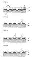
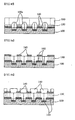
- a dielectric mask pattern 140 is formed on the first nitride semiconductor thin film 130 in such a manner that the first nitride semiconductor thin film 130 grown on the stripe-shaped grooves are masked and the first nitride semiconductor thin film 130 grown on the regions where the stripe-shaped grooves are not formed are exposed.
Landscapes
- Led Devices (AREA)
- Crystals, And After-Treatments Of Crystals (AREA)
Claims (8)
- Procédé pour faire croître un mince film semi-conducteur au nitrure ayant un moindre nombre de défauts, comprenant :une première étape consistant à former une couche tampon (120) sur une entière surface supérieure d'un substrat (100) avec des gorges en forme de ruban (110a) formées périodiquement sur celle-ci ;une seconde étape consistant à faire croître un premier film mince semi-conducteur au nitrure (130) sur la couche tampon (120) ;caractérisé parune troisième étape consistant à former un motif masque diélectrique (140) sur le premier film mince semi-conducteur au nitrure (130) de telle façon que le premier film mince semi-conducteur au nitrure qui a cru sur des régions du substrat (100) où les gorges en forme de ruban (110a) sont formées est masqué et le premier film mince semi-conducteur au nitrure (130) qui a cru sur des régions du substrat où les gorges en forme de ruban ne sont pas formées est exposé ;une quatrième étape consistant à attaquer des régions du premier film mince semi-conducteur au nitrure (130) qui sont exposées à travers le motif masque diélectrique (140), pour donner un motif en ruban périodique en saillie du premier film mince semi-conducteur au nitrure,et à supprimer le motif masque diélectrique depuis le premier film mince semi-conducteur au nitrure ; etune cinquième étape consistant à faire croître latéralement un second film mince semi-conducteur au nitrure (150) sur le motif du premier film mince semi-conducteur au nitrure (130a).
- Procédé selon la revendication 1, dans lequel le substrat (100) avec les gorges en forme de ruban formées périodiquement sur celui-ci est fabriqué :en formant le motif masque diélectrique (140) sur le substrat (100) de telle façon que le substrat est exposé à intervalles réguliers (d2) ;en attaquant le substrat (100), qui est exposé à travers le motif masque diélectrique (140), à une profondeur prédéterminée (d3) ; eten supprimant le motif masque diélectrique (140) depuis le substrat (100).
- Procédé selon la revendication 2, dans lequel l'intervalle (d2) est dans une plage de 0,1 à 15,0 µm.
- Procédé selon la revendication 2, dans lequel la profondeur du substrat (100) à attaquer est dans une plage de 0,1 à 10,0 µm.
- Procédé selon la revendication 2, dans lequel le substrat (100) est réalisé en un matériau sélectionné parmi un groupe comprenant carbure de silicium (SiC), saphir, arséniure de gallium (GaAs) et nitrure de gallium (GaN).
- Procédé selon la revendication 1, dans lequel la couche tampon (120) est réalisée d'une couche quelconque parmi une couche de AlxGayIn1-x-yN (0≤x≤1, 0≤y≤1, 0≤x+y≤1), une couche de SiN et un film stratifié avec la couche de AlxGayIn1-x-yN (0≤x≤1, 0≤y≤1, 0≤x+y≤1) et la couche de SiN stratifiée sur celle-ci.
- Procédé selon la revendication 1, dans lequel, après la seconde étape, le premier film mince semi-conducteur au nitrure (130) présente une densité de défauts plus élevée sur les régions dans lesquelles les gorges en forme de ruban (110a) ne sont pas formées et une densité de défauts plus faible sur les régions dans lesquelles les gorges en forme de ruban sont formées.
- Procédé selon la revendication 7, dans lequel le motif masque diélectrique (140) amène les régions à plus faible densité de défauts du premier film mince semi-conducteur au nitrure (130) à être masquées et les régions à plus forte densité de défauts du premier film mince semi-conducteur au nitrure à être exposées.
Applications Claiming Priority (2)
| Application Number | Priority Date | Filing Date | Title |
|---|---|---|---|
| KR10-2003-0101283A KR100512580B1 (ko) | 2003-12-31 | 2003-12-31 | 결함이 적은 질화물 반도체 박막 성장 방법 |
| KR2003101283 | 2003-12-31 |
Publications (3)
| Publication Number | Publication Date |
|---|---|
| EP1551056A2 EP1551056A2 (fr) | 2005-07-06 |
| EP1551056A3 EP1551056A3 (fr) | 2006-06-28 |
| EP1551056B1 true EP1551056B1 (fr) | 2015-02-11 |
Family
ID=34567865
Family Applications (1)
| Application Number | Title | Priority Date | Filing Date |
|---|---|---|---|
| EP04031027.8A Expired - Lifetime EP1551056B1 (fr) | 2003-12-31 | 2004-12-30 | Procédé de fabrication d'un film mince à nitrure de semiconducteur avec moins de défaults |
Country Status (5)
| Country | Link |
|---|---|
| US (2) | US7198971B2 (fr) |
| EP (1) | EP1551056B1 (fr) |
| JP (1) | JP4614125B2 (fr) |
| KR (1) | KR100512580B1 (fr) |
| CN (1) | CN1638041A (fr) |
Families Citing this family (28)
| Publication number | Priority date | Publication date | Assignee | Title |
|---|---|---|---|---|
| KR100512580B1 (ko) * | 2003-12-31 | 2005-09-06 | 엘지전자 주식회사 | 결함이 적은 질화물 반도체 박막 성장 방법 |
| JP5013661B2 (ja) * | 2004-03-31 | 2012-08-29 | 三洋電機株式会社 | 窒化物系半導体素子の製造方法及び窒化物系半導体素子 |
| KR100679610B1 (ko) * | 2006-01-16 | 2007-02-06 | 삼성전자주식회사 | 단결정 구조를 갖는 박막의 형성 방법 |
| TWI304278B (en) * | 2006-06-16 | 2008-12-11 | Ind Tech Res Inst | Semiconductor emitting device substrate and method of fabricating the same |
| TW200805452A (en) * | 2006-07-06 | 2008-01-16 | Nat Univ Chung Hsing | Method of making a low-defect-density epitaxial substrate and the product made therefrom |
| TWI464899B (zh) * | 2008-05-09 | 2014-12-11 | 榮創能源科技股份有限公司 | A method for manufacturing a semiconductor element |
| CN101587831B (zh) * | 2008-05-19 | 2013-01-16 | 展晶科技(深圳)有限公司 | 半导体元件结构及半导体元件的制造方法 |
| TWI425558B (zh) | 2008-08-11 | 2014-02-01 | 台灣積體電路製造股份有限公司 | 形成電路結構的方法 |
| US8803189B2 (en) * | 2008-08-11 | 2014-08-12 | Taiwan Semiconductor Manufacturing Company, Ltd. | III-V compound semiconductor epitaxy using lateral overgrowth |
| TW201029073A (en) * | 2009-01-21 | 2010-08-01 | Univ Nat Chunghsing | Epitaxial wafer with low surface defect density |
| KR101461684B1 (ko) * | 2009-02-24 | 2014-11-20 | 엘지전자 주식회사 | 질화물 반도체 발광 소자 및 그의 제조 방법 |
| US8039371B2 (en) * | 2009-07-01 | 2011-10-18 | International Business Machines Corporation | Reduced defect semiconductor-on-insulator hetero-structures |
| US8375349B2 (en) | 2009-09-02 | 2013-02-12 | Taiwan Semiconductor Manufacturing Company, Ltd. | Method for constant power density scaling |
| CN102054852A (zh) * | 2009-10-28 | 2011-05-11 | 展晶科技(深圳)有限公司 | 发光二极管及其制作方法 |
| US8759203B2 (en) * | 2009-11-17 | 2014-06-24 | Taiwan Semiconductor Manufacturing Company, Ltd. | Growing III-V compound semiconductors from trenches filled with intermediate layers |
| US8501597B2 (en) * | 2010-07-30 | 2013-08-06 | Academia Sinica | Method for fabricating group III-nitride semiconductor |
| TWI451480B (zh) * | 2010-10-08 | 2014-09-01 | Academia Sinica | 三族氮化物半導體之製造方法 |
| FR3022563B1 (fr) * | 2014-06-23 | 2016-07-15 | Univ Paris Xiii Paris-Nord Villetaneuse | Procede de formation d'un monocristal de materiau a partir d'un substrat monocristallin |
| WO2016018288A1 (fr) | 2014-07-30 | 2016-02-04 | Hewlett-Packard Development Company, L.P. | Dispositif multicouche hybride |
| DE102015107661B4 (de) * | 2015-05-15 | 2021-03-18 | OSRAM Opto Semiconductors Gesellschaft mit beschränkter Haftung | Verfahren zur Herstellung eines Nitridverbindungshalbleiter-Bauelements |
| US10658177B2 (en) | 2015-09-03 | 2020-05-19 | Hewlett Packard Enterprise Development Lp | Defect-free heterogeneous substrates |
| WO2017123245A1 (fr) | 2016-01-15 | 2017-07-20 | Hewlett Packard Enterprise Development Lp | Dispositif multicouche |
| WO2017171737A1 (fr) | 2016-03-30 | 2017-10-05 | Hewlett Packard Enterprise Development Lp | Dispositifs comprenant des substrats avec des régions d'entrefer sélectives |
| US10381801B1 (en) | 2018-04-26 | 2019-08-13 | Hewlett Packard Enterprise Development Lp | Device including structure over airgap |
| CN109616560A (zh) * | 2018-11-21 | 2019-04-12 | 江西兆驰半导体有限公司 | 一种适用于氮化物外延层生长的复合衬底 |
| CN113555283B (zh) * | 2020-04-24 | 2024-04-05 | 江苏鲁汶仪器股份有限公司 | 一种刻蚀GaN基高电子迁移率晶体管异质结的方法 |
| CN115552566B (zh) | 2020-05-27 | 2025-07-29 | 苏州晶湛半导体有限公司 | Ⅲ族氮化物结构及其制作方法 |
| CN112382709B (zh) * | 2020-12-03 | 2022-02-25 | 至芯半导体(杭州)有限公司 | 一种防裂纹的AlN外延层制造方法 |
Family Cites Families (17)
| Publication number | Priority date | Publication date | Assignee | Title |
|---|---|---|---|---|
| CA2258080C (fr) * | 1997-04-11 | 2007-06-05 | Nichia Chemical Industries, Ltd. | Procede assurant la croissance de semi-conducteurs de nitrure, substrat semi-conducteur de nitrure et dispositif semi-conducteur au nitrure. |
| US6608327B1 (en) * | 1998-02-27 | 2003-08-19 | North Carolina State University | Gallium nitride semiconductor structure including laterally offset patterned layers |
| US6265289B1 (en) * | 1998-06-10 | 2001-07-24 | North Carolina State University | Methods of fabricating gallium nitride semiconductor layers by lateral growth from sidewalls into trenches, and gallium nitride semiconductor structures fabricated thereby |
| JP4005701B2 (ja) * | 1998-06-24 | 2007-11-14 | シャープ株式会社 | 窒素化合物半導体膜の形成方法および窒素化合物半導体素子 |
| DE60043122D1 (de) * | 1999-03-17 | 2009-11-19 | Mitsubishi Chem Corp | Halbleiterbasis ihre Herstellung und Halbleiterkristallhersetllungsmethode |
| JP3555500B2 (ja) * | 1999-05-21 | 2004-08-18 | 豊田合成株式会社 | Iii族窒化物半導体及びその製造方法 |
| US6812053B1 (en) * | 1999-10-14 | 2004-11-02 | Cree, Inc. | Single step pendeo- and lateral epitaxial overgrowth of Group III-nitride epitaxial layers with Group III-nitride buffer layer and resulting structures |
| EP1104031B1 (fr) * | 1999-11-15 | 2012-04-11 | Panasonic Corporation | Diode laser à semiconducteur en nitrure et son procédé de fabrication |
| US6521514B1 (en) * | 1999-11-17 | 2003-02-18 | North Carolina State University | Pendeoepitaxial methods of fabricating gallium nitride semiconductor layers on sapphire substrates |
| JP4547746B2 (ja) * | 1999-12-01 | 2010-09-22 | ソニー株式会社 | 窒化物系iii−v族化合物の結晶製造方法 |
| JP4432180B2 (ja) * | 1999-12-24 | 2010-03-17 | 豊田合成株式会社 | Iii族窒化物系化合物半導体の製造方法、iii族窒化物系化合物半導体素子及びiii族窒化物系化合物半導体 |
| US6403451B1 (en) * | 2000-02-09 | 2002-06-11 | Noerh Carolina State University | Methods of fabricating gallium nitride semiconductor layers on substrates including non-gallium nitride posts |
| EP1265273A4 (fr) * | 2000-03-14 | 2009-05-06 | Toyoda Gosei Kk | Procede de production de semiconducteur a base de compose de nitrure iii et element en semiconducteur a base de compose de nitrure iii |
| US6627974B2 (en) * | 2000-06-19 | 2003-09-30 | Nichia Corporation | Nitride semiconductor substrate and method for manufacturing the same, and nitride semiconductor device using nitride semiconductor substrate |
| JP3679720B2 (ja) * | 2001-02-27 | 2005-08-03 | 三洋電機株式会社 | 窒化物系半導体素子および窒化物系半導体の形成方法 |
| EP1276140A3 (fr) * | 2001-07-04 | 2007-10-24 | FUJIFILM Corporation | Substrat présentant une large région à faible densité de défauts pour un élément semiconducteur |
| KR100512580B1 (ko) * | 2003-12-31 | 2005-09-06 | 엘지전자 주식회사 | 결함이 적은 질화물 반도체 박막 성장 방법 |
-
2003
- 2003-12-31 KR KR10-2003-0101283A patent/KR100512580B1/ko not_active Expired - Fee Related
-
2004
- 2004-12-28 JP JP2004380053A patent/JP4614125B2/ja not_active Expired - Fee Related
- 2004-12-29 US US11/023,540 patent/US7198971B2/en not_active Expired - Fee Related
- 2004-12-30 EP EP04031027.8A patent/EP1551056B1/fr not_active Expired - Lifetime
- 2004-12-31 CN CNA2004101031516A patent/CN1638041A/zh active Pending
-
2007
- 2007-03-20 US US11/725,498 patent/US20070190678A1/en not_active Abandoned
Also Published As
| Publication number | Publication date |
|---|---|
| JP4614125B2 (ja) | 2011-01-19 |
| EP1551056A2 (fr) | 2005-07-06 |
| US20070190678A1 (en) | 2007-08-16 |
| US20050139857A1 (en) | 2005-06-30 |
| KR20050069315A (ko) | 2005-07-05 |
| EP1551056A3 (fr) | 2006-06-28 |
| CN1638041A (zh) | 2005-07-13 |
| JP2005197721A (ja) | 2005-07-21 |
| US7198971B2 (en) | 2007-04-03 |
| KR100512580B1 (ko) | 2005-09-06 |
Similar Documents
| Publication | Publication Date | Title |
|---|---|---|
| EP1551056B1 (fr) | Procédé de fabrication d'un film mince à nitrure de semiconducteur avec moins de défaults | |
| US6100104A (en) | Method for fabricating a plurality of semiconductor bodies | |
| US7291509B2 (en) | Method for fabricating a plurality of semiconductor chips | |
| EP1104031B1 (fr) | Diode laser à semiconducteur en nitrure et son procédé de fabrication | |
| US8652918B2 (en) | Nitride semiconductor structure | |
| US6815241B2 (en) | GaN structures having low dislocation density and methods of manufacture | |
| US6362515B2 (en) | GaN substrate including wide low-defect region for use in semiconductor element | |
| US8877652B2 (en) | Substrate structure and method of manufacturing the same | |
| US20050156175A1 (en) | High quality nitride semiconductor thin film and method for growing the same | |
| JP2005314121A (ja) | 単結晶サファイア基板とその製造方法及び半導体発光素子 | |
| JP2002008985A (ja) | 窒化物半導体の製造方法及び窒化物半導体基板 | |
| US7122847B2 (en) | Nitride semiconductor thin film and method for growing the same | |
| US7294520B2 (en) | Method for fabricating a plurality of semiconductor bodies, and electronic semiconductor body | |
| KR100454907B1 (ko) | 질화물 반도체 기판 및 그의 제조 방법 | |
| KR100425680B1 (ko) | 질화물 반도체 박막 형성방법 | |
| KR20030061317A (ko) | 3-5족 화합물 반도체의 제조방법 및 반도체 소자 | |
| JP3823781B2 (ja) | 窒化物半導体基板およびその製造方法 | |
| KR100454908B1 (ko) | 질화갈륨 기판의 제조방법 | |
| KR100720537B1 (ko) | 질화물 반도체막 성장 방법 | |
| JP2001274517A (ja) | 半導体素子用基板およびその製造方法およびその半導体素子用基板を用いた半導体素子 |
Legal Events
| Date | Code | Title | Description |
|---|---|---|---|
| PUAI | Public reference made under article 153(3) epc to a published international application that has entered the european phase |
Free format text: ORIGINAL CODE: 0009012 |
|
| 17P | Request for examination filed |
Effective date: 20041230 |
|
| AK | Designated contracting states |
Kind code of ref document: A2 Designated state(s): AT BE BG CH CY CZ DE DK EE ES FI FR GB GR HU IE IS IT LI LT LU MC NL PL PT RO SE SI SK TR |
|
| AX | Request for extension of the european patent |
Extension state: AL BA HR LV MK YU |
|
| PUAL | Search report despatched |
Free format text: ORIGINAL CODE: 0009013 |
|
| AK | Designated contracting states |
Kind code of ref document: A3 Designated state(s): AT BE BG CH CY CZ DE DK EE ES FI FR GB GR HU IE IS IT LI LT LU MC NL PL PT RO SE SI SK TR |
|
| AX | Request for extension of the european patent |
Extension state: AL BA HR LV MK YU |
|
| AKX | Designation fees paid |
Designated state(s): FR GB NL |
|
| REG | Reference to a national code |
Ref country code: DE Ref legal event code: 8566 |
|
| 17Q | First examination report despatched |
Effective date: 20081222 |
|
| GRAP | Despatch of communication of intention to grant a patent |
Free format text: ORIGINAL CODE: EPIDOSNIGR1 |
|
| INTG | Intention to grant announced |
Effective date: 20140812 |
|
| GRAS | Grant fee paid |
Free format text: ORIGINAL CODE: EPIDOSNIGR3 |
|
| GRAA | (expected) grant |
Free format text: ORIGINAL CODE: 0009210 |
|
| AK | Designated contracting states |
Kind code of ref document: B1 Designated state(s): FR GB NL |
|
| REG | Reference to a national code |
Ref country code: GB Ref legal event code: FG4D |
|
| REG | Reference to a national code |
Ref country code: NL Ref legal event code: T3 |
|
| PLBE | No opposition filed within time limit |
Free format text: ORIGINAL CODE: 0009261 |
|
| STAA | Information on the status of an ep patent application or granted ep patent |
Free format text: STATUS: NO OPPOSITION FILED WITHIN TIME LIMIT |
|
| 26N | No opposition filed |
Effective date: 20151112 |
|
| GBPC | Gb: european patent ceased through non-payment of renewal fee |
Effective date: 20151230 |
|
| REG | Reference to a national code |
Ref country code: NL Ref legal event code: MM Effective date: 20160101 |
|
| REG | Reference to a national code |
Ref country code: FR Ref legal event code: ST Effective date: 20160831 |
|
| PG25 | Lapsed in a contracting state [announced via postgrant information from national office to epo] |
Ref country code: GB Free format text: LAPSE BECAUSE OF NON-PAYMENT OF DUE FEES Effective date: 20151230 Ref country code: NL Free format text: LAPSE BECAUSE OF NON-PAYMENT OF DUE FEES Effective date: 20160101 |
|
| PG25 | Lapsed in a contracting state [announced via postgrant information from national office to epo] |
Ref country code: FR Free format text: LAPSE BECAUSE OF NON-PAYMENT OF DUE FEES Effective date: 20151231 |