EP1551066A1 - Material mit strukturoberfläche zur verwendung als vorlage und prozess seiner herstellung - Google Patents
Material mit strukturoberfläche zur verwendung als vorlage und prozess seiner herstellung Download PDFInfo
- Publication number
- EP1551066A1 EP1551066A1 EP03797648A EP03797648A EP1551066A1 EP 1551066 A1 EP1551066 A1 EP 1551066A1 EP 03797648 A EP03797648 A EP 03797648A EP 03797648 A EP03797648 A EP 03797648A EP 1551066 A1 EP1551066 A1 EP 1551066A1
- Authority
- EP
- European Patent Office
- Prior art keywords
- compound
- group
- fluorine
- carbon atoms
- functional
- Prior art date
- Legal status (The legal status is an assumption and is not a legal conclusion. Google has not performed a legal analysis and makes no representation as to the accuracy of the status listed.)
- Withdrawn
Links
Images

Classifications
-
- B—PERFORMING OPERATIONS; TRANSPORTING
- B82—NANOTECHNOLOGY
- B82Y—SPECIFIC USES OR APPLICATIONS OF NANOSTRUCTURES; MEASUREMENT OR ANALYSIS OF NANOSTRUCTURES; MANUFACTURE OR TREATMENT OF NANOSTRUCTURES
- B82Y10/00—Nanotechnology for information processing, storage or transmission, e.g. quantum computing or single electron logic
-
- G—PHYSICS
- G03—PHOTOGRAPHY; CINEMATOGRAPHY; ANALOGOUS TECHNIQUES USING WAVES OTHER THAN OPTICAL WAVES; ELECTROGRAPHY; HOLOGRAPHY
- G03F—PHOTOMECHANICAL PRODUCTION OF TEXTURED OR PATTERNED SURFACES, e.g. FOR PRINTING, FOR PROCESSING OF SEMICONDUCTOR DEVICES; MATERIALS THEREFOR; ORIGINALS THEREFOR; APPARATUS SPECIALLY ADAPTED THEREFOR
- G03F7/00—Photomechanical, e.g. photolithographic, production of textured or patterned surfaces, e.g. printing surfaces; Materials therefor, e.g. comprising photoresists; Apparatus specially adapted therefor
- G03F7/0002—Lithographic processes using patterning methods other than those involving the exposure to radiation, e.g. by stamping
-
- B—PERFORMING OPERATIONS; TRANSPORTING
- B82—NANOTECHNOLOGY
- B82Y—SPECIFIC USES OR APPLICATIONS OF NANOSTRUCTURES; MEASUREMENT OR ANALYSIS OF NANOSTRUCTURES; MANUFACTURE OR TREATMENT OF NANOSTRUCTURES
- B82Y40/00—Manufacture or treatment of nanostructures
-
- H—ELECTRICITY
- H10—SEMICONDUCTOR DEVICES; ELECTRIC SOLID-STATE DEVICES NOT OTHERWISE PROVIDED FOR
- H10K—ORGANIC ELECTRIC SOLID-STATE DEVICES
- H10K71/00—Manufacture or treatment specially adapted for the organic devices covered by this subclass
- H10K71/10—Deposition of organic active material
- H10K71/191—Deposition of organic active material characterised by provisions for the orientation or alignment of the layer to be deposited
-
- Y—GENERAL TAGGING OF NEW TECHNOLOGICAL DEVELOPMENTS; GENERAL TAGGING OF CROSS-SECTIONAL TECHNOLOGIES SPANNING OVER SEVERAL SECTIONS OF THE IPC; TECHNICAL SUBJECTS COVERED BY FORMER USPC CROSS-REFERENCE ART COLLECTIONS [XRACs] AND DIGESTS
- Y10—TECHNICAL SUBJECTS COVERED BY FORMER USPC
- Y10T—TECHNICAL SUBJECTS COVERED BY FORMER US CLASSIFICATION
- Y10T428/00—Stock material or miscellaneous articles
- Y10T428/24—Structurally defined web or sheet [e.g., overall dimension, etc.]
- Y10T428/24802—Discontinuous or differential coating, impregnation or bond [e.g., artwork, printing, retouched photograph, etc.]
- Y10T428/24917—Discontinuous or differential coating, impregnation or bond [e.g., artwork, printing, retouched photograph, etc.] including metal layer
-
- Y—GENERAL TAGGING OF NEW TECHNOLOGICAL DEVELOPMENTS; GENERAL TAGGING OF CROSS-SECTIONAL TECHNOLOGIES SPANNING OVER SEVERAL SECTIONS OF THE IPC; TECHNICAL SUBJECTS COVERED BY FORMER USPC CROSS-REFERENCE ART COLLECTIONS [XRACs] AND DIGESTS
- Y10—TECHNICAL SUBJECTS COVERED BY FORMER USPC
- Y10T—TECHNICAL SUBJECTS COVERED BY FORMER US CLASSIFICATION
- Y10T428/00—Stock material or miscellaneous articles
- Y10T428/24—Structurally defined web or sheet [e.g., overall dimension, etc.]
- Y10T428/24802—Discontinuous or differential coating, impregnation or bond [e.g., artwork, printing, retouched photograph, etc.]
- Y10T428/24926—Discontinuous or differential coating, impregnation or bond [e.g., artwork, printing, retouched photograph, etc.] including ceramic, glass, porcelain or quartz layer
Definitions
- the present invention relates to a material with a pattern surface for used as a template, and a method for producing the same.
- H. Sirringhaus et al. developed a technique wherein a partition measuring 50 nm in height and 5 ⁇ m in width made of hydrophobic polyimide is provided on a glass substrate and an aqueous conductive polymer solution is applied in the partition by an ink-jet method to form an electrically conductive polymer thin film having a width of 10 ⁇ m.
- this method had a problem that the process is complicated because the partition is provided.
- JP-A-2002-261048 discloses a technique wherein a pattern surface having regions each having different affinity to a functional liquid is formed by using fluoroalkylsilane as a surface-treating agent and a functional liquid is applied to the region having high affinity by utilizing a difference in affinity.
- fluoroalkylsilane are not described in detail in this document.
- the pattern surface surface-treated with the straight-chain perfluoroalkyltrichlorosilane had such a problem that a difference in the region coated selectively with the functional liquid is not clear.
- JP-A-2000-307172, JP-A-7-206599 and JP-A-2001-94107 disclose techniques wherein performances of an organic semiconductor are improved by applying the organic semiconductor on a substrate surface-treated with a fluorine compound. However, there was such a problem that performances of the organic semiconductor are slightly improved.
- An object of the present invention is to enable the production of an anisotropic material having an alternating-line pattern structure by a simple process of applying an organic solvent liquid.
- a functional compound solution attains the wetting, which is faithful to an alternating-line pattern structure, on the surface of a substrate used as a template. That is, the functional compound solution spreads to wet one region of alternating lines on the substrate, and then a medium is vaporized to form a thin film of the functional compound in an alternating line shape.
- Another object of the present invention is to produce a structure of a functional compound of nanometer to micrometer order by a process of applying a functional compound solution by using, as a template, a pattern surface composed of plural regions each having different surface free energy.
- Still another object of the present invention is to apply a functional compound such as organic semiconductor to a pattern surface, at least one region of which is surface-treated with a fluorine compound, thereby improving properties of the functional compound.
- the present invention provides an anisotropic material comprising an alternating-line pattern and a layer of at least one functional compound selected from the group consisting of a semiconductor compound, an electrically conductive compound, a photochromic compound and a thermochromic compound, formed on the surface of the alternating-line pattern, wherein one type of lines comprises a first component comprising a fluorine-containing compound or silicone and the other type of lines comprises a second component comprising the other compound in the alternating-line pattern surface.
- the present invention provides a method for producing a functional material, comprising using, as a template, a pattern surface composed of plural regions each having different surface free energy, characterized in that:
- the present invention provides a method for producing a functional material, which comprises applying a functional compound to a pattern surface having at least one region surface-treated with a fluorine compound.
- one type of lines are made of a first component comprising a fluorine compound or silicone and the other one type of lines are made of a second component comprising the other compound.
- Examples of the base material constituting the alternating-line pattern include silicon, synthetic resin, glass, metal, and ceramics.
- the synthetic resin may be either a thermoplastic resin or a thermosetting resin and examples thereof include various thermoplastic elastomers, for example, polyolefins such as polyethylene, polypropylene, ethylene-propylene copolymer, and ethylene-vinyl acetate copolymer (EVA); cyclic polyolefin, modified polyolefin, polyvinyl chloride, polyvinylidene chloride, polystyrene, polyamide, polyimide, polyamideimide, polycarbonate, poly-(4-methylpentene-1), ionomer, acrylic resin, polymethyl methacrylate, acrylic-styrene copolymer (AS resin), butadiene-styrene copolymer, polyol copolymer (EVOH), polyesters such as polyethylene terephthalate (PET), polybutylene terephthalate (PBT) and polycyclohexane terephthalate (PCT); polyether, polyether ketone
- the glass examples include silica glass (quartz glass), alkali-silicate glass, soda-lime glass, potash-lime glass, lead (alkali) glass, barium glass, and borosilicate glass.
- Examples of the metal include gold, silver, copper, iron, nickel, aluminum, and platinum.
- the ceramic examples include oxides (for example, aluminum oxide, zinc oxide, titanium oxide, silicon oxide, zirconia, and barium titanate), nitrides (for example, silicon nitride and boron nitride), sulfides (for example, cadmium sulfide), and carbides (for example, silicon carbide), and a mixture thereof may be used.
- oxides for example, aluminum oxide, zinc oxide, titanium oxide, silicon oxide, zirconia, and barium titanate
- nitrides for example, silicon nitride and boron nitride
- sulfides for example, cadmium sulfide
- carbides for example, silicon carbide
- a functional group may be introduced into the surface of the substrate by plasma treatment or UV treatment.
- the compound used to form the alternating-line pattern on the surface of the base material may be an organic silane compound, an organic thiol compound, an organic disulfide compound, or an organic phosphate ester compound. That is, lines made of a fluorine-containing compound or silicone and lines made of the other compound can be formed from an organic silane compound, an organic thiol compound, an organic disulfide compound, or an organic phosphate ester compound.
- a difference between surface free energy of lines made of a fluorine-containing compound or silicone and surface free energy of lines made of the other compound is preferably at least 5 mJ/m 2 , for example, at least 10 mJ/m 2 , particularly at least 20 mJ/m 2 .
- the line width of the alternating-line pattern may be from 0.5 ⁇ m to 100 ⁇ m, for example, from 1 ⁇ m to 20 ⁇ m.
- the line width may be constant or changed.
- the shape of lines may be either a straight line or a curved line.
- the functional compound solution may be allowed to move spontaneously along lines by providing lines having lower surface free energy with tilt of surface free energy.
- Tilt of surface free energy can be provided, for example, by the method of M. K. Chaudhury et al. [Science, 256, 1539 (1992)].
- unevenness of alternating lines when the region having affinity with the functional compound is indented to form a groove, it is easy to wet in a line shape, as a matter of course.
- unevenness In case of preparing a pattern surface with only a monomolecular film, unevenness is not more than 10 nm, and preferably not more than 2 nm. The unevenness can be substantially neglected as compared with a line width of micron order.
- a solution of a functional compound spreads to wet one region of alternating lines, as if the groove existed.
- the shape of droplets is preferably distorted longitudinally in a line direction when 2 ⁇ L of ethanol is gently dropped on a line pattern surface serving as a template used to prepare an anisotropic material.
- the degree of distortion is preferably at least 1.1, for example, at least 1.2, in terms of a ratio L/W of the length in a major axis (L) to the length in a minor axis (W) of droplets.
- Both lines of the alternating-line pattern surface used as a template may be made of a monomolecular film or not.
- the alternating-line pattern surface of the present invention is prepared by the method such as photolithography, microcontact printing, self-assembling method, or electron beam irradiation method, and the method is not specifically limited.
- Sugimura et al. reported that, when an organic silane monomolecular film formed on a silicon wafer as a substrate is irradiated with vacuum-ultraviolet light through a line-shaped photomask, the irradiated area is photodecomposed to form a silanol group, thus obtaining a line pattern surface in which organic silane regions and silanol group regions are alternately arranged.
- the alternating-line pattern is made of a first component and a second component.
- the first component is a fluorine-containing compound or silicone.
- the second component is a compound other than the fluorine-containing compound and silicone.
- fluorine-containing compound examples include a fluorine-containing organic silane compound, a fluorine-containing organic thiol compound, a fluorine-containing organic disulfide compound, and a fluorine-containing organic phosphate ester compound.
- Examples of the fluorine-containing group in the fluorine-containing compound include a fluoroalkyl group (particularly, a perfluoroalkyl group), and a perfluoropolyether group.
- the number of carbon atoms of the fluorine-containing group is normally form 1 to 20, for example, 1 to 10.
- silicone examples include dimethylpolysiloxane, methylphenylpolysiloxane, methylhydrogenpolysiloxane, and silicone resin, and these silicones may be modified with fluorine.
- the compound (the second component) other than the fluorine compound and silicone may be an organic silane compound, an organic thiol compound, an organic disulfide compound, and/or an organic phosphate ester compound, which is not fluorinated or siliconated.
- the other compound may be a compound which has neither a fluorine atom nor a SiO bond.
- the functional compound is a semiconductor compound, an electrically conductive compound, a photochromic compound, and/or a thermochromic compound.
- the functional compound used in the present invention is at least one selected from the group consisting of the semiconductor compound, the conductive compound, the photochromic compound and the thermochromic compound.
- the semiconductor compound is preferably an organic compound and examples thereof include a pentacene derivative, a polythiophene derivative, a phthalocyanine derivative, a polyfluorene derivative, poly(p-phenylenevinylene), and a layered perovskite compound.
- the conductive compound has conductivity of at least 10 2 S/cm at room temperature and is preferably an organic compound, and examples thereof include a polyacetylene derivative, a polythiophene derivative, polypyrrole, poly(p-phenylenevinylene), and polyaniline.
- the conductivity may be improved by doping these compounds.
- the photochromic compound is preferably an organic compound and examples thereof include an azobenzene derivative, a spiropyran derivative, a fulgide derivative, and a diarylethene derivative.
- thermochromic compound is a generic term of a compound wherein a color of a substance varies reversibly with a change in temperature, and examples thereof include salicylideneanilines, a polythiophene derivative, a tetrahalogeno complex, an ethylenediamine derivative complex, a dinitrodiammine-copper complex, a 1,4-ziazacyclooctane (daco) complex, a hexamethylenetetramine (hmta) complex, and a salicylaldehyde (salen) complex.
- the thickness of a layer of the functional compound may be from 0.1 nm to 100 ⁇ m, for example, from 1 nm to 1 ⁇ m.
- the layer of the functional compound can be formed by applying a solution prepared by dissolving the functional compound in a solvent on the surface of a line pattern and removing the solvent.
- the solvent include an organic solvent and water. In case that the functional compound is slightly soluble in water, it must be dissolved in the organic solvent.
- the solvent used to dissolve the functional compound is preferably a solvent having a surface tension of not more than 30 mN/m, for example, not more than 20 mN/m.
- the surface tension is not more than 30 mN/m, the solution easily spreads to wet along lines.
- the organic solvent examples include alcohols, esters, ketones, ethers, and hydrocarbons (for example, aliphatic hydrocarbons and aromatic hydrocarbons) and the organic solvent may be fluorinated or not.
- Specific examples of the organic solvent include methanol, ethanol, isopropanol, perfluorodecalin, hydrofluoroether, HCFC225, chloroform, 1,1,2,2-tetrachloroethane, tetrachloroethylene, chlorobenzene, ethyl acetate, butyl acetate, acetone, hexane, isopentane, toluene, xylene, and tetrahydrofuran.
- the concentration of the functional compound in the solution may be from 0.1 to 20% by weight, for example, from 1 to 10% by weight.
- the solvent can be removed by vaporization.
- the solvent can be removed by heating an anisotropic material, for example, to a temperature of 60 to 200°C.
- the solvent may be removed under reduced pressure (for example, 0.01 to 100 Pa).
- examples of the method of applying the functional compound solution include a spin coating method, a dip coating method, a casting method, a roll coating method, a printing method, a transfer method, an ink-jet printing method [P. Calvert, Chem. Mater., 13, 3299 (2001)], a bar coating method, and a capillary method.
- the anisotropic material (that is, the functional material) of the present invention can be used as an electronic device in transistors, memories, light emitting diodes (EL), lasers and solar batteries, and is also used as an optical device in optical memories, image memories, light modulation elements, optical shutters, secondary harmonic (SHG) devices and polarizers.
- EL light emitting diodes
- SHG secondary harmonic
- a functional material is produced by a method wherein a pattern surface prepared by using the fluorine compound as a surface-treating agent is used as a template and a functional compound solution is applied, and then a solvent is removed.
- a functional material as a structure of a functional compound of nanometer to micrometer order for example, size of about 10 nm to 100 ⁇ m (for example, width (particularly, maximum width or minimum width) or diameter) is obtained.
- the pattern shape is not limited to line
- the functional compound is not limited to a semiconductor compound, an electrically conductive compound, a photochromic compound or a thermochromic compound, and a fluorine compound is used to prepare a pattern surface.
- the shape of the pattern surface may be selected according to the purposes of the finally produced device. Examples of the shape include circle, quadrangle, triangle, straight line, and curved line. Patterns may be contacted or separated with each other.
- the pattern surface is characterized by comprising at least two kinds of regions each having different surface free energy, at least one region being surface-treated with a fluorine compound.
- Examples of the functional compound include a semiconductor compound, a conductive compound, a photochromic compound, a thermochromic compound, a magnetic compound, and a bioactive compound.
- the fluorine compound used to prepare a pattern surface is preferably a fluorine compound having the following structures:
- the fluoroalkyl group in the fluorine compound may be a perfluoroalkyl group (having 1 to 5 carbon atoms).
- fluorine compound examples include a fluorine-containing organic silane compound, a fluorine-containing organic thiol compound, a fluorine-containing organic disulfide compound, and a fluorine-containing organic phosphate ester compound.
- a silane group (-SX 3 (wherein X is a hydrogen atom, a halogen atom or an oxyalkyl group (having 1 to 4 carbon atoms)
- a thiol group -SH
- a disulfide group -S-S-
- examples of the branched fluoroalkyl group include (CF 3 ) 2 CF-, (CF 3 ) 3 C-, (CF 3 ) 2 CFCF 2 CF 2 -, and (CF 3 ) 3 CCF 2 -.
- the fluorine compound (a) is a compound having a branched fluoroalkyl group and a functional group (for example, a silane group).
- examples of the perfluoropolyether group include the following: C a F 2a+1 O(CF 2 CF 2 CF 2 O) m (CF 2 ) 1 -, C a F 2a+1 O(CF 2 CF(CF 3 )O) m (CF 2 ) 1 -, C a F 2a+1 O(CF 2 CF 2 CF 2 O) m (CF 2 O) n (CF 2 ) 1 -, and C a F 2a+1 O(CF 2 CF(CF 3 )O) m (CF 2 O) n (CF 2 ) 1 - wherein a molecular weight of a perfluoropolyether group is at least 300, preferably at least 500, and not more than 100000, for example, not more than 5000, m and n represent 1 to 100, and preferably 20 to 40, a represents 1 to 10, and 1 represents 1 or 2.
- PFPE-A-SiX 3 examples include the followings: PFPE-A-SiX 3 , and PFPE-A-SH wherein PFPE is a perfluoropolyether group, A is an alkylene group having 1 to 4 carbon atoms, a -SO 2 N(R
- PFPE-CH 2 CH 2 -Si(OCH 3 ) 3 PFPE-SO 2 N(C 2 H 5 )CH 2 CH 2 -Si(OCH 3 ) 3
- PFPE-CH 2 CH 2 -SH PFPE-CH 2 CH 2 -SH.
- fluorine compound (c) having a polymer structure obtained by polymerizing a monomer which has a fluoroalkyl group having 5 or less carbon atoms examples include CF 3 -, CF 3 CF 2 -, CF 3 CF 2 CF 2 -, (CF 3 ) 2 CF-, CF 3 CF 2 CF 2 CF 2 -, (CF 3 ) 2 CFCF 2 -, (CF 3 ) 3 C-, CF 3 CF 2 CF 2 CF 2 -, (CF 3 ) 2 CFCF 2 CF 2 -, and (CF 3 ) 3 CCF 2 -.
- the monomer having a fluoroalkyl group is a compound having a fluoroalkyl group and a carbon-carbon double bond.
- the monomer having a fluoroalkyl group may be a fluoroalkyl group-containing vinyl monomer.
- the fluoroalkyl group-containing vinyl monomer may be a (meth)acrylate having a fluoroalkyl group, or an acrylate in which hydrogen at the ⁇ -position having a fluoroalkyl group is substituted with a halogen atom, CF 3 , CF 2 H or CFH 2 .
- Examples of A include an alkylene group having 1 to 4 carbon atoms, a -SO 2 N(R 21 )R 22 - group (provided that R 21 is an alkyl group having 1 to 4 carbon atoms, and R 22 is an alkylene group having 1 to 4 carbon atoms) and a -CH 2 CH(OH)CH 2 - group.
- Examples of the polymer structure obtained by polymerizing a monomer which has a fluoroalkyl group having 5 or less carbon atoms include the followings: - (Rf-A-OCOCR 3 CH 2 ) n - wherein Rf, A and R 3 are as defined above, and n is from 1 to 200, and particularly from 2 to 100.
- fluorine compound (c) examples include the followings:
- H(Rf-A-OCOCHCH 2 ) 4 -CH 2 CH 2 -Si(OCH 3 ) 3 H(Rf-A-OCOCHCHCl) 4 -CH 2 CH 2 -Si(OCH 3 ) 3 , H(Rf-A-OCOCHCHF) 4 -CH 2 CH 2 -SiCl 3 , H(Rf-A-OCOCClCH 2 ) 4 -CH 2 CH 2 -Si(OCH 3 ) 3
- H(Rf-A-OCOCFCH 2 ) 4 -CH 2 CH 2 -SiCl 3 H(Rf-A-OCOCFCH 2 ) 4 -CH 2 CH 2 -SiCl 3 .
- fluorine compound (d) having a linking group which is any one of an urethane group, an ester group, an ether group and an amide group, existing between a fluoroalkyl group having 5 or less carbon atoms and a functional group examples of the fluoroalkyl group having 5 or less carbon atoms are the same as those in the fluorine compound (c).
- fluorine compound (d) examples include the followings: Rf-A-OCONH-A'-SiX 3 , Rf-A-OCONH-A'-SH, Rf-A-NHCOO-A'-SiX 3 , Rf-A-NHCOO-A'-SH, Rf-A-OCO-A'-SiX 3 , Rf-A-OCO-A'-SH, Rf-A-COO-A'-SiX 3 , Rf-A-COO-A'-SH, Rf-A-O-A'-SiX 3 , Rf-A-O-A'-SH, Rf-A-CONH-A'-SiX 3 , Rf-A-CONH-A'-SH, and Rf-A-NHCO-A'-SH.
- Rf represents a fluoroalkyl group having 5 or less carbon atoms
- a and A' represent an alkylene group having 1 to 4 carbon atoms, a -SO 2 N(R 21 )R 22 - group (provided that R 21 is an alkyl group having 1 to 4 carbon atoms, and R 22 is an alkylene group having 1 to 4 carbon atoms) or a - CH 2 CH(OH)CH 2 - group
- Rf-CH 2 CH 2 -OCONH-CH 2 CH 2 CH 2 - (OCH 3 ) 3 examples thereof include the followings: Rf-CH 2 CH 2 -OCONH-CH 2 CH 2 CH 2 - (OCH 3 ) 3 , Rf-CH 2 CH 2 -OCONH-CH 2 CH 2 CH 2 -SH, Rf-CH 2 CH 2 -NHCOO-CH 2 CH 2 CH 2 -(OCH 3 ) 3 , Rf-CH 2 CH 2 -NBCOO-CH 2 CH 2 CH 2 -SH, Rf-CH 2 CH 2 -OCO-CH 2 CH 2 CH 2 -SiCl 3 , Rf-CH 2 CH 2 -OCO-CH 2 CH 2 CH 2 -SH, Rf-CH 2 CH 2 -COO-CH 2 CH 2 CH 2 - (OCH 3 ) 3 , Rf-CH 2 CH 2 -COO-CH 2 CH 2 CH 2 - (OCH 3 ) 3 , Rf-CH 2 CH 2
- the incompletely-condensed silsesquioxane (e) may be represented by the general formula: [R-Si (OH) O 2/2 ] l [R'-SiO 3/2 ] m wherein R and R' represent Rf, Rf-A, an alkyl group (having 1 to 22 carbon atoms), or a derivative of an alkyl group (having 1 to 22 carbon atoms) (provided that at least one of R and R' is Rf or Rf-A) (wherein Rf represents a fluoroalkyl group having 5 or less carbon atoms, and A represents an alkylene group having 1 to 4 carbon atoms, a -SO 2 N(R 21 )R 22 - group (provided that R 21 is an alkyl group having 1 to 4 carbon atoms, and R 22 is an alkylene group having 1 to 4 carbon atoms) or a -CH 2 CH(OH)CH 2 - group), and 1 and m represent such a number that a
- the silsesquioxane is also referred to as POSS (Polyhedral Oligomeric Silsesquioxane).
- a silanol group of the incompletely-condensed silsesquioxane has high reactivity and is therefore linked strongly with an active OH group of the substrate.
- the number of the silanol group in the molecule is from 1 to 3. 1 is normally from 1 to 3.
- m is normally at least 1, for example, at least 2, and particularly at least 3.
- incompletely-condensed silsesquioxane (e) examples include: and POSS Silanols 54,456-6 manufactured by Aldrich Co.
- fluoroalkyl group having 5 or less carbon atoms are the same as those in the fluorine compound (c).
- the completely-condensed silsesquioxane (f) may be represented by the formula: [R-SiO 3/2 ] l [R'-SiO 3/2 ] m wherein R represents Rf, Rf-A, an alkyl group (having 1 to 22 carbon atoms), or a derivative of an alkyl group (having 1 to 22 carbon atoms) (provided that at least one of R is Rf or Rf-A) (wherein Rf represents a fluoroalkyl group having 5 or less carbon atoms, A represents an alkylene group having 1 to 4 carbon atoms, a -SO 2 N(R 21 )R 22 - group (provided that R 21 is an alkyl group having 1 to 4 carbon atoms, and R 22 is an alkylene group having 1 to 4 carbon atoms) or a - CH 2 CH(OH)CH 2 - group), R' represents an organic group containing SiX 3 , for example, -(CH 2 ) n
- the completely-condensed silsesquioxane (f) can be obtained by condensing an incompletely-condensed silsesquioxane (e) with bis-silane.
- bis-silane examples include the followings:
- a functional material is obtained by using, as a template, a pattern surface, at least one region of which is surface-treated with a fluorine compound, and applying a functional compound such as organic semiconductor on the template.
- a functional compound such as organic semiconductor
- the method of applying the functional compound to the pattern surface is not specifically limited as far as it is a method of contacting the functional compound with the pattern surface, and a method capable of improving properties of the functional compound as highly as possible may be appropriately selected regardless of solid phase, liquid phase or vapor phase.
- Examples of the application method include a friction transfer method, a spin coating method, a casting method, an ink-jet method, a dipping method, a vacuum deposition method, and a sputtering method.
- An organic silane as a first component is chemically adsorbed on the silicon wafer.
- the silicon wafer is irradiated with vacuum-ultraviolet light (172 nm) through a line-shaped photomask (line width: 0.1 ⁇ m, 1 ⁇ m, 5 ⁇ m, and 10 ⁇ m)
- the irradiated organic area is photodecomposed to form a silanol group, thus obtaining a line pattern surface in which organic silane regions and silanol group regions are alternately arrayed.
- Reagents used to prepare the respective surfaces are as follows: Rf is perfluorohexylethyltrimethoxysilane (manufactured by Fluorochem Ltd.), Rh(C 18 ) is n-octadecyltrimethoxysilane (manufactured by CHISSO CORPORATION), and Rh(C 10 ) is n-decyltriethoxysilane (manufactured by CHISSO CORPORATION).
- Formation of the objective pattern was confirmed by a lateral force microscope.
- Pattern surfaces shown in Table 2 were prepared.
- first component/second component was described.
- Difference in surface free energy is a difference in surface free energy of a sole monomolecular film determined in Table 1.
- Line width was measured by a lateral force microscope.
- Unevenness of alternating lines denotes a difference between a molecular length of the first component and a molecular length of the second component, and was measured by an atomic force microscope.
- a 1 wt% functional compound solution shown in Table 3 was applied thereon.
- the spin coating was performed at 2000 rpm, and the dip coating was performed by fixing a substrate in a direction in which lines of a pattern are vertical to the solution surface, and the dipping and pull-up operations were performed at a rate of 1 mm/second.
- Examples 1 to 5 it was confirmed by an optical microscope and an atomic force microscope that a thin film (120 nm thick) of a functional compound is formed in an alternating line shape on the pattern surface used as the template.
- a uniform thin film (140 nm thick) of a functional compound was formed on the entire surface of the substrate without constituting a line.
- ADS2000P sodium poly[2-(3-thienyl)ethyloxy-4-butylsulfonate]
- a fluorine organic silane shown in Table 4 was chemically adsorbed in a liquid phase by the following method.
- the organic silane was diluted with a soluble dehydrated organic solvent, and then a silicon wafer was dipped in the resulting 1 wt% solution for one hour. After dipping, the silicon wafer was washed with the same organic solvent and dried in an atmospheric air to prepare a sole monomolecular film of the fluorine organic silane alone.
- a contact angle and surface free energy of the sole monomolecular film, which is not a pattern surface, were also shown in Table 4.
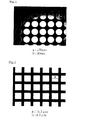
- the resulting sole monomolecular film was irradiated with vacuum-ultraviolet light (wavelength: 172 nm) through a photomask having each shape shown in Figs. 1 to 4 (circle, quadrangle, triangle and line) to form a silanol group in the irradiated area.
- vacuum-ultraviolet light wavelength: 172 nm
- dark areas represent the masked regions.
- the resulting pattern surface is shown in Table 5. Formation of the objective pattern was confirmed by a field emission scanning electron microscope (FE-SEM).
- Examples 7 to 17 of the present invention it was confirmed by an optical microscope and an atomic force microscope that a thin film of a functional compound is formed in a shape, which is the same as that of the pattern surface, on the pattern surface used as the template (150 nm thick). The thin film was formed only in the SiOH region. In Comparative Example 5, a uniform thin film (140 nm thick) of the functional compound was formed on the entire surface of the substrate, regardless of the shape of the pattern surface.
- a fluorine organic silane Rf-POSS1 shown in Table 4 was chemically adsorbed in a liquid phase by the same method as in Preparation Example 7. Then, the silicon wafer was irradiated with vacuum-ultraviolet light (172 nm) through a line-shaped photomask shown in Fig. 4 to form a silanol group in the irradiated area. Formation of the objective pattern was confirmed by FE-SEM. In Example 18, a 1 wt% poly(3-hexylthiophene) solution was dropped on the pattern surface by using an ink-jet apparatus produced by us. Ink-jet conditions are as follows.
- a microdroplet having a diameter of several tens of ⁇ m was prepared one by one by an on-demand system and then dropped at intervals of 1 mm.
- the microdroplet was dropped by the ink-jet apparatus on Rh(C10)/SO 3 H having a line width of 10 ⁇ m (Comparative Preparation Example 2 shown in Table 2) in the same manner as in Example 18.
- the shape of the poly(3-hexylthiophene) thin film formed on the pattern surface was observed by an optical microscope. As a result, it has been found that a thin film was formed in a line shape, which is faithful to the line shape having a line width of 10 ⁇ m, was formed in Example 18.
- the thin film was formed only at the SiOH region.
- a circular thin film having a diameter of about 100 ⁇ m was formed, regardless of lines of the pattern surface.
- a fluorine organic silane Rf-POSS1 shown in Table 4 was chemically adsorbed in a liquid phase in the same manner as in Preparation Example 7. Then, the silicon wafer was irradiated with vacuum-ultraviolet light (172 nm) through a line-shaped photomask shown in Fig. 4 to form a silanol group in the irradiated area. Formation of the objective pattern was confirmed by FE-SEM. In Example 19, using this pattern surface as a template, pentacene was vapor-deposited on the pattern surface (150 nm thick). In Comparative Example 7, pentacene was vapor-deposited on an untreated silicon wafer (160 nm thick). In both cases, pentacene was vapor-deposited at a substrate temperature of 200°C.
- source and drain electrodes of gold were formed on the substrate by a vacuum deposition method.
- the source and drain electrodes were disposed vertically to lines of the substrate.
- the thickness of the gold vapor-deposited film was set to 100 nm.
- a distance (channel length) L between the source and drain electrodes was set to 10 ⁇ m and the length (channel width) W of the source and drain electrodes was set to 10 mm.
- an Al thin film for leading-out a gate electrode was vapor-deposited on the back surface of the silicon wafer to give an organic TFT comprising a pentacene vapor-deposited film.
- Mobility was 0.13 cm 2 /Vs in case of using the pattern surface as the substrate, while mobility was 0.005 cm 2 /Vs in case of using the untreated silicon wafer as the substrate.
- an anisotropic material having an alternating-line pattern structure can be produced by a simple application (or coating) process.
- a structure of a functional compound of nanometer to micrometer order can be produced by a simple application process.
- properties of a functional compound can be improved by using, as a template, the surface of a pattern, at least one region of which is surface-treated with a fluorine compound having a specific structure.
Landscapes
- Engineering & Computer Science (AREA)
- Nanotechnology (AREA)
- Chemical & Material Sciences (AREA)
- Physics & Mathematics (AREA)
- Crystallography & Structural Chemistry (AREA)
- General Physics & Mathematics (AREA)
- Condensed Matter Physics & Semiconductors (AREA)
- Manufacturing & Machinery (AREA)
- Mathematical Physics (AREA)
- Theoretical Computer Science (AREA)
- Application Of Or Painting With Fluid Materials (AREA)
- Laminated Bodies (AREA)
- Thin Film Transistor (AREA)
- Moulds For Moulding Plastics Or The Like (AREA)
Applications Claiming Priority (3)
| Application Number | Priority Date | Filing Date | Title |
|---|---|---|---|
| JP2002273144 | 2002-09-19 | ||
| JP2002273144 | 2002-09-19 | ||
| PCT/JP2003/011876 WO2004027889A1 (ja) | 2002-09-19 | 2003-09-18 | パターン表面をテンプレートとして用いる材料とその製法 |
Publications (2)
| Publication Number | Publication Date |
|---|---|
| EP1551066A1 true EP1551066A1 (de) | 2005-07-06 |
| EP1551066A4 EP1551066A4 (de) | 2009-01-14 |
Family
ID=32024945
Family Applications (1)
| Application Number | Title | Priority Date | Filing Date |
|---|---|---|---|
| EP03797648A Withdrawn EP1551066A4 (de) | 2002-09-19 | 2003-09-18 | Material mit strukturoberfläche zur verwendung als vorlage und prozess seiner herstellung |
Country Status (7)
| Country | Link |
|---|---|
| US (1) | US20060159849A1 (de) |
| EP (1) | EP1551066A4 (de) |
| JP (1) | JP4325555B2 (de) |
| CN (1) | CN100477319C (de) |
| AU (1) | AU2003264479A1 (de) |
| TW (1) | TW200408324A (de) |
| WO (1) | WO2004027889A1 (de) |
Cited By (4)
| Publication number | Priority date | Publication date | Assignee | Title |
|---|---|---|---|---|
| US8158728B2 (en) | 2004-02-13 | 2012-04-17 | The University Of North Carolina At Chapel Hill | Methods and materials for fabricating microfluidic devices |
| US8263129B2 (en) | 2003-12-19 | 2012-09-11 | The University Of North Carolina At Chapel Hill | Methods for fabricating isolated micro-and nano-structures using soft or imprint lithography |
| US8268446B2 (en) | 2003-09-23 | 2012-09-18 | The University Of North Carolina At Chapel Hill | Photocurable perfluoropolyethers for use as novel materials in microfluidic devices |
| US9040090B2 (en) | 2003-12-19 | 2015-05-26 | The University Of North Carolina At Chapel Hill | Isolated and fixed micro and nano structures and methods thereof |
Families Citing this family (25)
| Publication number | Priority date | Publication date | Assignee | Title |
|---|---|---|---|---|
| JP4865999B2 (ja) * | 2004-11-19 | 2012-02-01 | 株式会社日立製作所 | 電界効果トランジスタの作製方法 |
| US20060204766A1 (en) * | 2005-03-14 | 2006-09-14 | Jds Uniphase Corporation | Anti-moisture and soil-repellent coatings |
| US8138075B1 (en) | 2006-02-06 | 2012-03-20 | Eberlein Dietmar C | Systems and methods for the manufacture of flat panel devices |
| JP4961819B2 (ja) * | 2006-04-26 | 2012-06-27 | 株式会社日立製作所 | 電界効果トランジスタ及びその製造方法 |
| JP2008106165A (ja) * | 2006-10-26 | 2008-05-08 | Chisso Corp | インクジェット用インクおよび当該インクにより得られる硬化膜 |
| US8058463B2 (en) | 2007-12-04 | 2011-11-15 | E. I. Du Pont De Nemours And Compnay | Fluorosilanes |
| US8153834B2 (en) * | 2007-12-05 | 2012-04-10 | E.I. Dupont De Nemours And Company | Surface modified inorganic particles |
| CN102105987B (zh) * | 2008-07-22 | 2013-04-03 | Dic株式会社 | 有机晶体管及其制造方法 |
| JP5197497B2 (ja) * | 2009-06-03 | 2013-05-15 | 三菱レイヨン株式会社 | 一軸水平配向ミクロ相分離構造を有するブロック共重合体薄膜の製造方法 |
| JP5752987B2 (ja) * | 2011-05-09 | 2015-07-22 | 三菱レイヨン株式会社 | 液晶性ブロック共重合体塗膜、液晶性ブロック共重合体薄膜の製造方法及びパターン形成方法 |
| DE102013210138A1 (de) * | 2013-05-30 | 2014-12-04 | Boehringer Ingelheim Vetmedica Gmbh | Verfahren zum Erzeugen einer Vielzahl von Messbereichen auf einem Chip sowie Chip mit Messbereichen |
| JP2014236148A (ja) * | 2013-06-04 | 2014-12-15 | 東京エレクトロン株式会社 | 有機分子膜の形成装置および形成方法 |
| JP6406817B2 (ja) * | 2013-12-10 | 2018-10-17 | デクセリアルズ株式会社 | 硬化樹脂成形体 |
| JP2015205973A (ja) | 2014-04-18 | 2015-11-19 | キヤノンファインテック株式会社 | 撥水撥油性組成物、及びそれを用いて形成した撥水膜 |
| JP6381971B2 (ja) * | 2014-05-30 | 2018-08-29 | デクセリアルズ株式会社 | 表面自由エネルギー転写用光硬化性樹脂組成物、及びこれを用いた基板の製造方法 |
| CN107074580B (zh) * | 2014-10-17 | 2020-05-22 | 国立研究开发法人产业技术总合研究所 | 纳米晶体的排列方法、纳米晶体结构体的制作方法、纳米晶体结构体形成基板及纳米晶体结构体形成基板的制造方法 |
| JP6453622B2 (ja) * | 2014-11-21 | 2019-01-16 | デクセリアルズ株式会社 | 配線基板の製造方法、及び配線基板 |
| JP6193321B2 (ja) * | 2015-09-01 | 2017-09-06 | 株式会社東芝 | エッチング方法、物品の製造方法、及びエッチング装置 |
| EP3383537B1 (de) | 2015-12-02 | 2020-08-19 | Boehringer Ingelheim Vetmedica GmbH | Chip mit mehreren messbereichen |
| EP3663087A4 (de) * | 2017-08-04 | 2021-04-21 | Daikin Industries, Ltd. | Substrat zur musterbildung |
| CN109810573A (zh) * | 2017-11-21 | 2019-05-28 | Tcl集团股份有限公司 | 无机纳米材料印刷油墨及其制备方法和应用 |
| KR20210056411A (ko) * | 2018-10-10 | 2021-05-18 | 커먼웰쓰 사이언티픽 앤드 인더스트리얼 리서치 오가니제이션 | 광전자 장치용 페로브스카이트 필름 형성 방법 |
| JP7251770B2 (ja) * | 2019-02-07 | 2023-04-04 | 国立大学法人 筑波大学 | 有機マイクロ共振器、有機マイクロ共振器アレイ、偽造防止システム、スイッチング素子、有機マイクロ共振器の製造方法、有機マイクロ共振器アレイの製造方法 |
| CN111514811A (zh) * | 2020-03-26 | 2020-08-11 | 陕西驭腾实业有限公司 | 一种不对称Gemini氟碳表面活性剂的制备方法 |
| CN119709120B (zh) * | 2024-12-05 | 2025-11-18 | 国网北京市电力公司 | 改性石墨烯硅烷复合粘结剂及其制备方法与应用 |
Family Cites Families (14)
| Publication number | Priority date | Publication date | Assignee | Title |
|---|---|---|---|---|
| EP0166363B1 (de) * | 1984-06-26 | 1991-08-07 | Asahi Glass Company Ltd. | Durchsichtiger schwer schmutzender Gegenstand mit niedriger Reflexion |
| US5556706A (en) * | 1993-10-06 | 1996-09-17 | Matsushita Electric Industrial Co., Ltd. | Conductive layered product and method of manufacturing the same |
| US6265243B1 (en) * | 1999-03-29 | 2001-07-24 | Lucent Technologies Inc. | Process for fabricating organic circuits |
| JP3865106B2 (ja) * | 2000-03-31 | 2007-01-10 | セイコーエプソン株式会社 | シリコン膜パターンの形成方法 |
| JP4035752B2 (ja) * | 2000-03-31 | 2008-01-23 | セイコーエプソン株式会社 | 微細構造体の製造方法 |
| JP3921917B2 (ja) * | 2000-03-31 | 2007-05-30 | セイコーエプソン株式会社 | 微細構造体の製造方法 |
| JP3843706B2 (ja) * | 2000-07-04 | 2006-11-08 | セイコーエプソン株式会社 | 微細構造体の製造方法 |
| US20020081520A1 (en) * | 2000-12-21 | 2002-06-27 | Ratnam Sooriyakumaran | Substantially transparent aqueous base soluble polymer system for use in 157 nm resist applications |
| JP3625196B2 (ja) * | 2000-12-28 | 2005-03-02 | セイコーエプソン株式会社 | Rfidタグの形成方法、rfidタグの形成装置、スピーカの形成方法、およびスピーカの形成装置 |
| JP4000853B2 (ja) * | 2000-12-28 | 2007-10-31 | セイコーエプソン株式会社 | 分子膜パターンの形成方法、分子膜パターン、及び半導体装置の製造方法 |
| US6939665B2 (en) * | 2000-12-28 | 2005-09-06 | Seiko Epson Corporation | System and methods for manufacturing a molecular film pattern |
| JP2002261049A (ja) * | 2001-02-28 | 2002-09-13 | Mitsumi Electric Co Ltd | ダイシング装置及びダイシング方法 |
| US6973710B2 (en) * | 2001-08-03 | 2005-12-13 | Seiko Epson Corporation | Method and apparatus for making devices |
| JP4000836B2 (ja) * | 2001-11-28 | 2007-10-31 | セイコーエプソン株式会社 | 膜パターンの形成方法 |
-
2003
- 2003-09-18 AU AU2003264479A patent/AU2003264479A1/en not_active Abandoned
- 2003-09-18 JP JP2004537592A patent/JP4325555B2/ja not_active Expired - Fee Related
- 2003-09-18 CN CNB03822304XA patent/CN100477319C/zh not_active Expired - Fee Related
- 2003-09-18 US US10/528,376 patent/US20060159849A1/en not_active Abandoned
- 2003-09-18 TW TW092125712A patent/TW200408324A/zh unknown
- 2003-09-18 WO PCT/JP2003/011876 patent/WO2004027889A1/ja not_active Ceased
- 2003-09-18 EP EP03797648A patent/EP1551066A4/de not_active Withdrawn
Cited By (12)
| Publication number | Priority date | Publication date | Assignee | Title |
|---|---|---|---|---|
| US8268446B2 (en) | 2003-09-23 | 2012-09-18 | The University Of North Carolina At Chapel Hill | Photocurable perfluoropolyethers for use as novel materials in microfluidic devices |
| US8263129B2 (en) | 2003-12-19 | 2012-09-11 | The University Of North Carolina At Chapel Hill | Methods for fabricating isolated micro-and nano-structures using soft or imprint lithography |
| US8420124B2 (en) | 2003-12-19 | 2013-04-16 | The University Of North Carolina At Chapel Hill | Methods for fabricating isolated micro- and nano-structures using soft or imprint lithography |
| US8992992B2 (en) | 2003-12-19 | 2015-03-31 | The University Of North Carolina At Chapel Hill | Methods for fabricating isolated micro- or nano-structures using soft or imprint lithography |
| US9040090B2 (en) | 2003-12-19 | 2015-05-26 | The University Of North Carolina At Chapel Hill | Isolated and fixed micro and nano structures and methods thereof |
| US9877920B2 (en) | 2003-12-19 | 2018-01-30 | The University Of North Carolina At Chapel Hill | Methods for fabricating isolated micro- or nano-structures using soft or imprint lithography |
| US9902818B2 (en) | 2003-12-19 | 2018-02-27 | The University Of North Carolina At Chapel Hill | Isolated and fixed micro and nano structures and methods thereof |
| US10517824B2 (en) | 2003-12-19 | 2019-12-31 | The University Of North Carolina At Chapel Hill | Methods for fabricating isolated micro- or nano-structures using soft or imprint lithography |
| US10842748B2 (en) | 2003-12-19 | 2020-11-24 | The University Of North Carolina At Chapel Hill | Methods for fabricating isolated micro- or nano-structures using soft or imprint lithography |
| US11642313B2 (en) | 2003-12-19 | 2023-05-09 | The University Of North Carolina At Chapel Hill | Methods for fabricating isolated micro- or nano-structures using soft or imprint lithography |
| US8158728B2 (en) | 2004-02-13 | 2012-04-17 | The University Of North Carolina At Chapel Hill | Methods and materials for fabricating microfluidic devices |
| US8444899B2 (en) | 2004-02-13 | 2013-05-21 | The University Of North Carolina At Chapel Hill | Methods and materials for fabricating microfluidic devices |
Also Published As
| Publication number | Publication date |
|---|---|
| WO2004027889A1 (ja) | 2004-04-01 |
| JPWO2004027889A1 (ja) | 2006-01-19 |
| AU2003264479A1 (en) | 2004-04-08 |
| TW200408324A (en) | 2004-05-16 |
| JP4325555B2 (ja) | 2009-09-02 |
| EP1551066A4 (de) | 2009-01-14 |
| US20060159849A1 (en) | 2006-07-20 |
| CN100477319C (zh) | 2009-04-08 |
| CN1682388A (zh) | 2005-10-12 |
Similar Documents
| Publication | Publication Date | Title |
|---|---|---|
| US20060159849A1 (en) | Material with pattern surface for use as template and process for producing the same | |
| US5512328A (en) | Method for forming a pattern and forming a thin film used in pattern formation | |
| Rozsnyai et al. | Selective electrochemical deposition of polyaniline via photopatterning of a monolayer-modified substrate | |
| US6887332B1 (en) | Patterning solution deposited thin films with self-assembled monolayers | |
| US7491286B2 (en) | Patterning solution deposited thin films with self-assembled monolayers | |
| US7923110B2 (en) | Metal nanoparticle having a self-assembled monolayer on its surface, and formation of conductive pattern using the same | |
| JP4331256B2 (ja) | 有機分子膜構造体の形成方法 | |
| US20050263025A1 (en) | Micro-contact printing method | |
| CN100480739C (zh) | 微镜、微镜阵列及其制造方法 | |
| US7875320B2 (en) | Method for producing film of vanadium pentoxide nanowires having improved alignment and vanadium pentoxide nanowire film produced thereby | |
| US20140346141A1 (en) | Self-assemblable polymer and methods for use in lithography | |
| JP3921917B2 (ja) | 微細構造体の製造方法 | |
| EP0523503A2 (de) | Ultradünner Polymerfilm-Elektret und Verfahren zu seiner Herstellung | |
| EP2775543B1 (de) | Verfahren zur Herstellung eines Transistors mit Nanopartikeln mit wesentlich gleichförmigem Anordnungsmuster | |
| EP0511650B1 (de) | Antistatische Folie und Verfahren zur Herstellung | |
| Bae et al. | A Nonconventional Approach to Patterned Nanoarrays of DNA Strands for Template‐Assisted Assembly of Polyfluorene Nanowires | |
| CA2060629C (en) | Magnetic recording medium and method of manufacturing the same | |
| US20120080679A1 (en) | Alkylsilane laminate, production method thereof and thin-film transistor | |
| US7579086B2 (en) | Substrate for use in crystallization and method for producing the same | |
| JPWO2005091070A1 (ja) | リソグラフィー用基板表面処理剤 | |
| KR102283716B1 (ko) | 불소 함유 양친매성 유무기하이브리드 복합체 및 이를 이용한 유기박막 트랜지스터 | |
| US8106387B2 (en) | Organic thin film transistors | |
| EP1831764A2 (de) | Auf sam-wachstum basierende nanoproduktion | |
| US20070145371A1 (en) | Thin-film transistor | |
| JPH02307572A (ja) | 均斉薄膜の形成方法 |
Legal Events
| Date | Code | Title | Description |
|---|---|---|---|
| PUAI | Public reference made under article 153(3) epc to a published international application that has entered the european phase |
Free format text: ORIGINAL CODE: 0009012 |
|
| 17P | Request for examination filed |
Effective date: 20050418 |
|
| AK | Designated contracting states |
Kind code of ref document: A1 Designated state(s): AT BE BG CH CY CZ DE DK EE ES FI FR GB GR HU IE IT LI LU MC NL PT RO SE SI SK TR |
|
| AX | Request for extension of the european patent |
Extension state: AL LT LV MK |
|
| DAX | Request for extension of the european patent (deleted) | ||
| A4 | Supplementary search report drawn up and despatched |
Effective date: 20081211 |
|
| RIC1 | Information provided on ipc code assigned before grant |
Ipc: G03F 7/075 20060101ALI20081205BHEP Ipc: G03F 7/004 20060101ALI20081205BHEP Ipc: H01L 51/00 20060101AFI20040408BHEP |
|
| 17Q | First examination report despatched |
Effective date: 20110114 |
|
| STAA | Information on the status of an ep patent application or granted ep patent |
Free format text: STATUS: THE APPLICATION IS DEEMED TO BE WITHDRAWN |
|
| 18D | Application deemed to be withdrawn |
Effective date: 20110525 |