EP1551106A2 - RF-Modul für ein Mobilkommunikationsendgerät - Google Patents
RF-Modul für ein Mobilkommunikationsendgerät Download PDFInfo
- Publication number
- EP1551106A2 EP1551106A2 EP04030897A EP04030897A EP1551106A2 EP 1551106 A2 EP1551106 A2 EP 1551106A2 EP 04030897 A EP04030897 A EP 04030897A EP 04030897 A EP04030897 A EP 04030897A EP 1551106 A2 EP1551106 A2 EP 1551106A2
- Authority
- EP
- European Patent Office
- Prior art keywords
- board
- module structure
- mcm
- component
- mobile communication
- Prior art date
- Legal status (The legal status is an assumption and is not a legal conclusion. Google has not performed a legal analysis and makes no representation as to the accuracy of the status listed.)
- Granted
Links
- 238000010295 mobile communication Methods 0.000 title claims abstract description 16
- 239000000919 ceramic Substances 0.000 claims abstract description 19
- 239000004593 Epoxy Substances 0.000 claims description 6
- 239000002184 metal Substances 0.000 claims description 5
- 238000000465 moulding Methods 0.000 claims description 5
- 238000010030 laminating Methods 0.000 claims description 4
- 239000000463 material Substances 0.000 claims description 3
- 238000004891 communication Methods 0.000 abstract description 2
- 230000005540 biological transmission Effects 0.000 description 8
- 238000000034 method Methods 0.000 description 5
- 230000000694 effects Effects 0.000 description 3
- 229920003258 poly(methylsilmethylene) Polymers 0.000 description 3
- SWPMTVXRLXPNDP-UHFFFAOYSA-N 4-hydroxy-2,6,6-trimethylcyclohexene-1-carbaldehyde Chemical compound CC1=C(C=O)C(C)(C)CC(O)C1 SWPMTVXRLXPNDP-UHFFFAOYSA-N 0.000 description 2
- 238000001816 cooling Methods 0.000 description 2
- IRLPACMLTUPBCL-KQYNXXCUSA-N 5'-adenylyl sulfate Chemical compound C1=NC=2C(N)=NC=NC=2N1[C@@H]1O[C@H](COP(O)(=O)OS(O)(=O)=O)[C@@H](O)[C@H]1O IRLPACMLTUPBCL-KQYNXXCUSA-N 0.000 description 1
- 238000002296 dynamic light scattering Methods 0.000 description 1
- 238000012986 modification Methods 0.000 description 1
- 230000004048 modification Effects 0.000 description 1
- 230000002093 peripheral effect Effects 0.000 description 1
- 238000013061 process characterization study Methods 0.000 description 1
Images

Classifications
-
- H—ELECTRICITY
- H04—ELECTRIC COMMUNICATION TECHNIQUE
- H04B—TRANSMISSION
- H04B1/00—Details of transmission systems, not covered by a single one of groups H04B3/00 - H04B13/00; Details of transmission systems not characterised by the medium used for transmission
- H04B1/38—Transceivers, i.e. devices in which transmitter and receiver form a structural unit and in which at least one part is used for functions of transmitting and receiving
- H04B1/40—Circuits
-
- H—ELECTRICITY
- H04—ELECTRIC COMMUNICATION TECHNIQUE
- H04B—TRANSMISSION
- H04B1/00—Details of transmission systems, not covered by a single one of groups H04B3/00 - H04B13/00; Details of transmission systems not characterised by the medium used for transmission
- H04B1/38—Transceivers, i.e. devices in which transmitter and receiver form a structural unit and in which at least one part is used for functions of transmitting and receiving
Definitions
- the present invention relates to a mobile communication terminal, and particularly, to an RF multi-chip module of a mobile communication terminal.
- Figure 1 is a configuration view of a general mobile communication terminal.
- a mobile communication terminal includes an RF (Radio Frequency) system 10, a base-band system 20 and an additional device 30.
- RF Radio Frequency
- the RF system 10 includes an antenna, a transmission unit, a reception unit and a local oscillator (LO), and the base-band system 20 includes an MSM (Mobile Station Modem) chip corresponding to a CPU (Central Processing Unit) of a computer; a memory and peripheral devices.
- MSM Mobile Station Modem
- the additional device 30 is a part for provding a user with an output signal of the base-band system 20 or transmitting a signal inputted by a user to the base-band system 20 and generally includes a speaker, a microphone, a keypad, an LCD, a camera and the like.
- the RF system 10 and the base-band system 20 are integrated on one board.
- the RF system and the base-band system are integrated on one board, according to an area having a different frequency band (range), the RF system has to be re-designed to correspond to a frequency range of the corresponding area. That is, the related art is disadvantageous in that a board has to be individually designed when a frequency band (PCS, CDMA, AMPS ) is different, even though the base band chipset is the same.
- PCS frequency band
- CDMA Code Division Multiple Access
- AMPS base band chipset
- an object of the present invention is to provide an RF multi-chip module (RF MCM) obtained by separately modularizing the RF part of a mobile communication terminal which includes an RF part and a base-band part.
- RF MCM RF multi-chip module
- Another object of the present invention is to provide an RF module structure of a mobile communication terminal allowing an RF board to be easily replaced according to the desired frequency band to be used.
- an RF module structure of a mobile communication terminal including an RF part and a base-band part, wherein the base-band part is commonly used, and the RF part is replaceably modularized into one RF multi-chip module (RF MCM).
- RF MCM RF multi-chip module
- the RF MCM is implemented in one of a lead free type, a lead type and a connector type.
- the RF MCM includes a board; a plurality of RF components mounted on the board; and a cap for isolating the RF components from the exterior environment.
- the board can be implemented by a low temperature co-fired ceramic (LTCC) and a high co-fired ceramic (HTCC) which are types of ceramic laminated boards and general FR4 PCB laminated board.
- LTCC low temperature co-fired ceramic
- HTCC high co-fired ceramic
- the cap is formed by epoxy molding or shield metal.
- each RF component is a component in a bare-die state and is wire-bonded on the board.
- each RF component is a modularized component and is soldered on the board.
- an RF board has to be individually designed according to a frequency (PCSs, CDMA and Tri-Mode) even though a base-band chipset is the same in fabricating a mobile communication terminal.
- the present invention proposes an RF Multi-Chip Module (MCM) obtained by separately modularizing the RF part of a mobile communication terminal which includes an RF part and a base-band part. That is, in the present invention, the RF system of a mobile communication terminal is integrated into one chip.
- MCM RF Multi-Chip Module
- a base-band part is commonly used according to a chipset and then a proper RF MCM is replaceably inserted thereto according to the frequency used in the specific area, so that a terminal can be easily fabricated in a short amount of time without the need for designing a new RF board.
- Figure 2 is a sectional view of an RF MCM in accordance with an embodiment of the present invention.
- the RF MCM in accordance with the present invention includes a plurality of wires formed at an upper surface of a board 50, for allowing signals to be transferred; a transmission unit 52 and a reception unit 53 separately mounted on the board 50; and a cap 54 for isolating the transmission unit 52 and the reception unit 53 from the exterior environment.
- the board 50 is formed by a low temperature co-fired ceramic (LTCC) and a high co-fired ceramic (HTCC) which are types of ceramic laminated boards and general FR4 PCB laminated board (two-sided Epoxy), and the cap 30 is implemented by using epoxy molding or shield metal.
- LTCC low temperature co-fired ceramic
- HTCC high co-fired ceramic
- the cap 30 is implemented by using epoxy molding or shield metal.
- the FR-4 used as a multi-layer board is used as a material of the board 50 for the RF MCM, and wires for mounting a chip on the board 50, that is, wires 51 for separately mounting a transmission unit 52 and a reception unit 53 are formed on the board.
- LTCC formed by laminating ceramic sheets may be used for the board 50.
- the LTCC is a kind of ceramic board formed by laminating ceramic sheets. Since a dielectric constant of the LTCC is nearly twice as high as that of FR-4, the size of the board can be reduced. In addition, since the LTCC has good heat conductivity, the large amount of heat generated by a PAM (Power Amplifier Module) can be efficiently released, whereby the cooling effect which reduces the temperature of the mobile terminal itself.
- PAM Power Amplifier Module
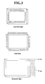
- the RF MCM is divided into a lead free type and a lead type according to the type of pins, whereby other types of connectors instead of pins may also be used.
- reference number 60 is a connector in a connector type RF MCM and reference number 61 is a cap.
- an RF system can be implemented into an RF MCM by mounting the components on a board 50 having the above mentioned characteristics using various mounting methods.
- an operation of the RF MCM is the same as that of the RF system, and a board 50 used for the RF MCM is made of LTCC.
- each component in a bare-die state is wire-bonded to the LTCC to fabricate an RF MCM. That is, a transmission unit 52 and a reception unit 53 are positioned along the wires 51 of the board 50, and then wire-bonding is performed, to thereby fabricate an RF MCM.
- a transmission unit 52 and a reception unit 53 which have already been modularized are respectively positioned along the wires 51 and then are soldered, to thereby fabricate an RF MCM.
- the RF MCM is covered with a cap 54 so as to be isolated from the exterior environment.
- the cap 54 of the RF MCM is fabricated by a method of epoxy molding such as an IC package, or by covering the board with a shield can (metal) to block unwanted wave interference from the outside, and increasing ESD and GND effects.
- a base-band part is commonly used and then only the RF module is replaced for PCS, CDMA, Tri-Mode or the like which employ different frequencies, thereby providing a smooth communication service in various frequency band.
- an RF MCM using an LTCC board that is a ceramic laminated board (not a FR-4 board)
- the size of the board may be reduced, and also the generated heat of the board is effectively released, so that there can be a cooling effect that lowers the temperature of the mobile terminal itself.
Landscapes
- Engineering & Computer Science (AREA)
- Computer Networks & Wireless Communication (AREA)
- Signal Processing (AREA)
- Transceivers (AREA)
- Telephone Set Structure (AREA)
Applications Claiming Priority (2)
| Application Number | Priority Date | Filing Date | Title |
|---|---|---|---|
| KR2003100748 | 2003-12-30 | ||
| KR1020030100748A KR100631673B1 (ko) | 2003-12-30 | 2003-12-30 | 이동통신용 고주파 모듈 구조 |
Publications (3)
| Publication Number | Publication Date |
|---|---|
| EP1551106A2 true EP1551106A2 (de) | 2005-07-06 |
| EP1551106A3 EP1551106A3 (de) | 2009-02-25 |
| EP1551106B1 EP1551106B1 (de) | 2011-04-13 |
Family
ID=34567862
Family Applications (1)
| Application Number | Title | Priority Date | Filing Date |
|---|---|---|---|
| EP04030897A Expired - Lifetime EP1551106B1 (de) | 2003-12-30 | 2004-12-28 | RF-Modul für ein Mobilkommunikationsendgerät |
Country Status (6)
| Country | Link |
|---|---|
| US (1) | US7715203B2 (de) |
| EP (1) | EP1551106B1 (de) |
| KR (1) | KR100631673B1 (de) |
| CN (1) | CN1665378A (de) |
| AT (1) | ATE505851T1 (de) |
| DE (1) | DE602004032207D1 (de) |
Families Citing this family (5)
| Publication number | Priority date | Publication date | Assignee | Title |
|---|---|---|---|---|
| US10674611B2 (en) * | 2015-06-29 | 2020-06-02 | NagraID Security | Method of reducing the thickness of an electronic circuit |
| KR102480672B1 (ko) * | 2018-06-11 | 2022-12-27 | 가부시키가이샤 무라타 세이사쿠쇼 | 고주파 모듈 및 통신 장치 |
| CN111221390A (zh) * | 2019-12-31 | 2020-06-02 | 苏州浪潮智能科技有限公司 | 一种兼容分时连接CPU和Tri mode卡的背板及实现方法 |
| KR20220164305A (ko) | 2021-06-04 | 2022-12-13 | 삼성전자주식회사 | 전자 장치에서의 쉴드 구조 및 그 동작 방법 |
| US12268863B2 (en) | 2023-02-06 | 2025-04-08 | Novocure Gmbh | Shiftable transducer array with anisotropic material layer |
Citations (2)
| Publication number | Priority date | Publication date | Assignee | Title |
|---|---|---|---|---|
| WO2000045420A2 (en) | 1999-01-29 | 2000-08-03 | Conexant Systems, Inc. | Multiple chip module with integrated rf capabilities |
| US20020049042A1 (en) | 2000-06-20 | 2002-04-25 | Murata Manufacturing Co., Ltd. | RF module |
Family Cites Families (19)
| Publication number | Priority date | Publication date | Assignee | Title |
|---|---|---|---|---|
| JP3118266B2 (ja) * | 1990-03-06 | 2000-12-18 | ゼロックス コーポレイション | 同期セグメントバスとバス通信方法 |
| US5414214A (en) * | 1992-10-16 | 1995-05-09 | Motorola, Inc. | Resistance heated, sealed microfabricated device package method and apparatus |
| US5587885A (en) * | 1994-05-18 | 1996-12-24 | Dell Usa, L.P. | Mechanical printed circuit board/laminated multi chip module interconnect apparatus |
| AU4926396A (en) * | 1995-02-16 | 1996-09-04 | Micromodule Systems, Inc. | Multiple chip module mounting assembly and computer using same |
| US5841193A (en) * | 1996-05-20 | 1998-11-24 | Epic Technologies, Inc. | Single chip modules, repairable multichip modules, and methods of fabrication thereof |
| US5949654A (en) * | 1996-07-03 | 1999-09-07 | Kabushiki Kaisha Toshiba | Multi-chip module, an electronic device, and production method thereof |
| US5920464A (en) * | 1997-09-22 | 1999-07-06 | Trw Inc. | Reworkable microelectronic multi-chip module |
| US6897855B1 (en) * | 1998-02-17 | 2005-05-24 | Sarnoff Corporation | Tiled electronic display structure |
| JP3538045B2 (ja) | 1998-12-09 | 2004-06-14 | 三菱電機株式会社 | Rf回路モジュール |
| DE19927747C1 (de) * | 1999-06-17 | 2000-07-06 | Siemens Ag | Multichipmodul aus einem zusammenhängenden Waferscheibenteil für die LOC-Montage sowie Verfahren zu dessen Herstellung |
| JP2001177433A (ja) * | 1999-12-21 | 2001-06-29 | Murata Mfg Co Ltd | 高周波複合部品及び移動体通信装置 |
| CN1324168A (zh) | 2000-05-16 | 2001-11-28 | 仁宝电脑工业股份有限公司 | 无线通信接口的共用模块装置 |
| US7132841B1 (en) * | 2000-06-06 | 2006-11-07 | International Business Machines Corporation | Carrier for test, burn-in, and first level packaging |
| KR20020006055A (ko) * | 2000-07-11 | 2002-01-19 | 이형도 | 위상 동기 루프형 발진기 모듈 |
| US6891276B1 (en) * | 2002-01-09 | 2005-05-10 | Bridge Semiconductor Corporation | Semiconductor package device |
| US7181572B2 (en) * | 2002-12-02 | 2007-02-20 | Silverbrook Research Pty Ltd | Cache updating method and apparatus |
| TWI221333B (en) * | 2003-01-14 | 2004-09-21 | Advanced Semiconductor Eng | Bridge connection type of MCM package |
| CN2629355Y (zh) | 2003-01-30 | 2004-07-28 | 友旺科技股份有限公司 | 无线传输装置的印刷电路板结构 |
| US7186119B2 (en) * | 2003-10-17 | 2007-03-06 | Integrated System Technologies, Llc | Interconnection device |
-
2003
- 2003-12-30 KR KR1020030100748A patent/KR100631673B1/ko not_active Expired - Fee Related
-
2004
- 2004-12-28 DE DE602004032207T patent/DE602004032207D1/de not_active Expired - Lifetime
- 2004-12-28 EP EP04030897A patent/EP1551106B1/de not_active Expired - Lifetime
- 2004-12-28 AT AT04030897T patent/ATE505851T1/de not_active IP Right Cessation
- 2004-12-30 CN CN2004100997990A patent/CN1665378A/zh active Pending
- 2004-12-30 US US11/026,080 patent/US7715203B2/en not_active Expired - Fee Related
Patent Citations (2)
| Publication number | Priority date | Publication date | Assignee | Title |
|---|---|---|---|---|
| WO2000045420A2 (en) | 1999-01-29 | 2000-08-03 | Conexant Systems, Inc. | Multiple chip module with integrated rf capabilities |
| US20020049042A1 (en) | 2000-06-20 | 2002-04-25 | Murata Manufacturing Co., Ltd. | RF module |
Also Published As
| Publication number | Publication date |
|---|---|
| US20050143122A1 (en) | 2005-06-30 |
| US7715203B2 (en) | 2010-05-11 |
| CN1665378A (zh) | 2005-09-07 |
| EP1551106A3 (de) | 2009-02-25 |
| KR100631673B1 (ko) | 2006-10-09 |
| KR20050068930A (ko) | 2005-07-05 |
| ATE505851T1 (de) | 2011-04-15 |
| EP1551106B1 (de) | 2011-04-13 |
| DE602004032207D1 (de) | 2011-05-26 |
Similar Documents
| Publication | Publication Date | Title |
|---|---|---|
| WO2022209755A1 (ja) | 高周波モジュール | |
| US7515879B2 (en) | Radio frequency circuit module | |
| CN100372241C (zh) | 以多层陶瓷形成的射频收发模块 | |
| EP2416544B1 (de) | Elektromagnetische Abschirmung und akustische Kammer eines Mikrofons in einer mobilen elektronischen Vorrichtung | |
| KR20010082044A (ko) | 패키지화 된 집적 회로 | |
| US20130095897A1 (en) | Electromagnetic shielding and an acoustic chamber for a microphone in a mobile electronic device | |
| CN115004560B (zh) | 阻抗匹配收发器 | |
| US12355413B2 (en) | Cap substrate for acoustic wave device | |
| EP1551106A2 (de) | RF-Modul für ein Mobilkommunikationsendgerät | |
| US11757476B2 (en) | Radio frequency module and communication device | |
| US11431360B2 (en) | Radio-frequency module and communication device | |
| US12341540B2 (en) | Radio frequency circuit, radio frequency module, and communication device | |
| US12588555B2 (en) | Dual sided molded package with varying interconnect pad sizes and varying exposed solderable area | |
| US20230155612A1 (en) | Radio frequency module and communication device | |
| WO2022209754A1 (ja) | 高周波モジュール | |
| WO2022209734A1 (ja) | 高周波モジュール及び通信装置 | |
| WO2022209756A1 (ja) | 高周波モジュール及び通信装置 | |
| JP3576465B2 (ja) | 高周波半導体装置およびそれを用いた携帯用通信機器 | |
| WO2022209740A1 (ja) | 高周波モジュール | |
| WO2022209742A1 (ja) | 高周波モジュール及び通信装置 | |
| WO2022209730A1 (ja) | 高周波モジュール | |
| WO2025204625A1 (ja) | 高周波モジュール、及び、通信装置 | |
| WO2022209741A1 (ja) | 高周波モジュール及び通信装置 | |
| KR20090023848A (ko) | 신호 처리 모듈 | |
| KR20050053828A (ko) | 통신 모듈 측정 장치 |
Legal Events
| Date | Code | Title | Description |
|---|---|---|---|
| PUAI | Public reference made under article 153(3) epc to a published international application that has entered the european phase |
Free format text: ORIGINAL CODE: 0009012 |
|
| 17P | Request for examination filed |
Effective date: 20041228 |
|
| AK | Designated contracting states |
Kind code of ref document: A2 Designated state(s): AT BE BG CH CY CZ DE DK EE ES FI FR GB GR HU IE IS IT LI LT LU MC NL PL PT RO SE SI SK TR |
|
| AX | Request for extension of the european patent |
Extension state: AL BA HR LV MK YU |
|
| PUAL | Search report despatched |
Free format text: ORIGINAL CODE: 0009013 |
|
| AK | Designated contracting states |
Kind code of ref document: A3 Designated state(s): AT BE BG CH CY CZ DE DK EE ES FI FR GB GR HU IE IS IT LI LT LU MC NL PL PT RO SE SI SK TR |
|
| AX | Request for extension of the european patent |
Extension state: AL BA HR LV MK YU |
|
| AKX | Designation fees paid |
Designated state(s): AT BE BG CH CY CZ DE DK EE ES FI FR GB GR HU IE IS IT LI LT LU MC NL PL PT RO SE SI SK TR |
|
| 17Q | First examination report despatched |
Effective date: 20100811 |
|
| GRAP | Despatch of communication of intention to grant a patent |
Free format text: ORIGINAL CODE: EPIDOSNIGR1 |
|
| GRAS | Grant fee paid |
Free format text: ORIGINAL CODE: EPIDOSNIGR3 |
|
| GRAA | (expected) grant |
Free format text: ORIGINAL CODE: 0009210 |
|
| RAP1 | Party data changed (applicant data changed or rights of an application transferred) |
Owner name: LG ELECTRONICS INC. |
|
| AK | Designated contracting states |
Kind code of ref document: B1 Designated state(s): AT BE BG CH CY CZ DE DK EE ES FI FR GB GR HU IE IS IT LI LT LU MC NL PL PT RO SE SI SK TR |
|
| REG | Reference to a national code |
Ref country code: GB Ref legal event code: FG4D |
|
| REG | Reference to a national code |
Ref country code: CH Ref legal event code: EP |
|
| REG | Reference to a national code |
Ref country code: IE Ref legal event code: FG4D |
|
| REF | Corresponds to: |
Ref document number: 602004032207 Country of ref document: DE Date of ref document: 20110526 Kind code of ref document: P |
|
| REG | Reference to a national code |
Ref country code: DE Ref legal event code: R096 Ref document number: 602004032207 Country of ref document: DE Effective date: 20110526 |
|
| REG | Reference to a national code |
Ref country code: NL Ref legal event code: VDEP Effective date: 20110413 |
|
| LTIE | Lt: invalidation of european patent or patent extension |
Effective date: 20110413 |
|
| PG25 | Lapsed in a contracting state [announced via postgrant information from national office to epo] |
Ref country code: LT Free format text: LAPSE BECAUSE OF FAILURE TO SUBMIT A TRANSLATION OF THE DESCRIPTION OR TO PAY THE FEE WITHIN THE PRESCRIBED TIME-LIMIT Effective date: 20110413 Ref country code: SE Free format text: LAPSE BECAUSE OF FAILURE TO SUBMIT A TRANSLATION OF THE DESCRIPTION OR TO PAY THE FEE WITHIN THE PRESCRIBED TIME-LIMIT Effective date: 20110413 Ref country code: PT Free format text: LAPSE BECAUSE OF FAILURE TO SUBMIT A TRANSLATION OF THE DESCRIPTION OR TO PAY THE FEE WITHIN THE PRESCRIBED TIME-LIMIT Effective date: 20110816 |
|
| PG25 | Lapsed in a contracting state [announced via postgrant information from national office to epo] |
Ref country code: FI Free format text: LAPSE BECAUSE OF FAILURE TO SUBMIT A TRANSLATION OF THE DESCRIPTION OR TO PAY THE FEE WITHIN THE PRESCRIBED TIME-LIMIT Effective date: 20110413 Ref country code: IS Free format text: LAPSE BECAUSE OF FAILURE TO SUBMIT A TRANSLATION OF THE DESCRIPTION OR TO PAY THE FEE WITHIN THE PRESCRIBED TIME-LIMIT Effective date: 20110813 Ref country code: BE Free format text: LAPSE BECAUSE OF FAILURE TO SUBMIT A TRANSLATION OF THE DESCRIPTION OR TO PAY THE FEE WITHIN THE PRESCRIBED TIME-LIMIT Effective date: 20110413 Ref country code: SI Free format text: LAPSE BECAUSE OF FAILURE TO SUBMIT A TRANSLATION OF THE DESCRIPTION OR TO PAY THE FEE WITHIN THE PRESCRIBED TIME-LIMIT Effective date: 20110413 Ref country code: CY Free format text: LAPSE BECAUSE OF FAILURE TO SUBMIT A TRANSLATION OF THE DESCRIPTION OR TO PAY THE FEE WITHIN THE PRESCRIBED TIME-LIMIT Effective date: 20110413 Ref country code: ES Free format text: LAPSE BECAUSE OF FAILURE TO SUBMIT A TRANSLATION OF THE DESCRIPTION OR TO PAY THE FEE WITHIN THE PRESCRIBED TIME-LIMIT Effective date: 20110724 Ref country code: AT Free format text: LAPSE BECAUSE OF FAILURE TO SUBMIT A TRANSLATION OF THE DESCRIPTION OR TO PAY THE FEE WITHIN THE PRESCRIBED TIME-LIMIT Effective date: 20110413 Ref country code: GR Free format text: LAPSE BECAUSE OF FAILURE TO SUBMIT A TRANSLATION OF THE DESCRIPTION OR TO PAY THE FEE WITHIN THE PRESCRIBED TIME-LIMIT Effective date: 20110714 |
|
| PG25 | Lapsed in a contracting state [announced via postgrant information from national office to epo] |
Ref country code: NL Free format text: LAPSE BECAUSE OF FAILURE TO SUBMIT A TRANSLATION OF THE DESCRIPTION OR TO PAY THE FEE WITHIN THE PRESCRIBED TIME-LIMIT Effective date: 20110413 |
|
| PG25 | Lapsed in a contracting state [announced via postgrant information from national office to epo] |
Ref country code: EE Free format text: LAPSE BECAUSE OF FAILURE TO SUBMIT A TRANSLATION OF THE DESCRIPTION OR TO PAY THE FEE WITHIN THE PRESCRIBED TIME-LIMIT Effective date: 20110413 Ref country code: CZ Free format text: LAPSE BECAUSE OF FAILURE TO SUBMIT A TRANSLATION OF THE DESCRIPTION OR TO PAY THE FEE WITHIN THE PRESCRIBED TIME-LIMIT Effective date: 20110413 |
|
| PLBE | No opposition filed within time limit |
Free format text: ORIGINAL CODE: 0009261 |
|
| STAA | Information on the status of an ep patent application or granted ep patent |
Free format text: STATUS: NO OPPOSITION FILED WITHIN TIME LIMIT |
|
| PG25 | Lapsed in a contracting state [announced via postgrant information from national office to epo] |
Ref country code: PL Free format text: LAPSE BECAUSE OF FAILURE TO SUBMIT A TRANSLATION OF THE DESCRIPTION OR TO PAY THE FEE WITHIN THE PRESCRIBED TIME-LIMIT Effective date: 20110413 Ref country code: RO Free format text: LAPSE BECAUSE OF FAILURE TO SUBMIT A TRANSLATION OF THE DESCRIPTION OR TO PAY THE FEE WITHIN THE PRESCRIBED TIME-LIMIT Effective date: 20110413 Ref country code: SK Free format text: LAPSE BECAUSE OF FAILURE TO SUBMIT A TRANSLATION OF THE DESCRIPTION OR TO PAY THE FEE WITHIN THE PRESCRIBED TIME-LIMIT Effective date: 20110413 Ref country code: DK Free format text: LAPSE BECAUSE OF FAILURE TO SUBMIT A TRANSLATION OF THE DESCRIPTION OR TO PAY THE FEE WITHIN THE PRESCRIBED TIME-LIMIT Effective date: 20110413 |
|
| 26N | No opposition filed |
Effective date: 20120116 |
|
| REG | Reference to a national code |
Ref country code: DE Ref legal event code: R097 Ref document number: 602004032207 Country of ref document: DE Effective date: 20120116 |
|
| PG25 | Lapsed in a contracting state [announced via postgrant information from national office to epo] |
Ref country code: IT Free format text: LAPSE BECAUSE OF FAILURE TO SUBMIT A TRANSLATION OF THE DESCRIPTION OR TO PAY THE FEE WITHIN THE PRESCRIBED TIME-LIMIT Effective date: 20110413 |
|
| PG25 | Lapsed in a contracting state [announced via postgrant information from national office to epo] |
Ref country code: MC Free format text: LAPSE BECAUSE OF NON-PAYMENT OF DUE FEES Effective date: 20111231 |
|
| REG | Reference to a national code |
Ref country code: CH Ref legal event code: PL |
|
| REG | Reference to a national code |
Ref country code: IE Ref legal event code: MM4A |
|
| PG25 | Lapsed in a contracting state [announced via postgrant information from national office to epo] |
Ref country code: CH Free format text: LAPSE BECAUSE OF NON-PAYMENT OF DUE FEES Effective date: 20111231 Ref country code: IE Free format text: LAPSE BECAUSE OF NON-PAYMENT OF DUE FEES Effective date: 20111228 Ref country code: LI Free format text: LAPSE BECAUSE OF NON-PAYMENT OF DUE FEES Effective date: 20111231 |
|
| PG25 | Lapsed in a contracting state [announced via postgrant information from national office to epo] |
Ref country code: LU Free format text: LAPSE BECAUSE OF NON-PAYMENT OF DUE FEES Effective date: 20111228 |
|
| PG25 | Lapsed in a contracting state [announced via postgrant information from national office to epo] |
Ref country code: BG Free format text: LAPSE BECAUSE OF FAILURE TO SUBMIT A TRANSLATION OF THE DESCRIPTION OR TO PAY THE FEE WITHIN THE PRESCRIBED TIME-LIMIT Effective date: 20110713 |
|
| PG25 | Lapsed in a contracting state [announced via postgrant information from national office to epo] |
Ref country code: TR Free format text: LAPSE BECAUSE OF FAILURE TO SUBMIT A TRANSLATION OF THE DESCRIPTION OR TO PAY THE FEE WITHIN THE PRESCRIBED TIME-LIMIT Effective date: 20110413 |
|
| PG25 | Lapsed in a contracting state [announced via postgrant information from national office to epo] |
Ref country code: HU Free format text: LAPSE BECAUSE OF FAILURE TO SUBMIT A TRANSLATION OF THE DESCRIPTION OR TO PAY THE FEE WITHIN THE PRESCRIBED TIME-LIMIT Effective date: 20110413 |
|
| REG | Reference to a national code |
Ref country code: FR Ref legal event code: PLFP Year of fee payment: 12 |
|
| PGFP | Annual fee paid to national office [announced via postgrant information from national office to epo] |
Ref country code: DE Payment date: 20151111 Year of fee payment: 12 Ref country code: GB Payment date: 20151111 Year of fee payment: 12 |
|
| PGFP | Annual fee paid to national office [announced via postgrant information from national office to epo] |
Ref country code: FR Payment date: 20151113 Year of fee payment: 12 |
|
| REG | Reference to a national code |
Ref country code: DE Ref legal event code: R119 Ref document number: 602004032207 Country of ref document: DE |
|
| GBPC | Gb: european patent ceased through non-payment of renewal fee |
Effective date: 20161228 |
|
| REG | Reference to a national code |
Ref country code: FR Ref legal event code: ST Effective date: 20170831 |
|
| PG25 | Lapsed in a contracting state [announced via postgrant information from national office to epo] |
Ref country code: FR Free format text: LAPSE BECAUSE OF NON-PAYMENT OF DUE FEES Effective date: 20170102 |
|
| PG25 | Lapsed in a contracting state [announced via postgrant information from national office to epo] |
Ref country code: DE Free format text: LAPSE BECAUSE OF NON-PAYMENT OF DUE FEES Effective date: 20170701 Ref country code: GB Free format text: LAPSE BECAUSE OF NON-PAYMENT OF DUE FEES Effective date: 20161228 |