EP1553418A1 - Capteur d'acceleration - Google Patents
Capteur d'acceleration Download PDFInfo
- Publication number
- EP1553418A1 EP1553418A1 EP03788112A EP03788112A EP1553418A1 EP 1553418 A1 EP1553418 A1 EP 1553418A1 EP 03788112 A EP03788112 A EP 03788112A EP 03788112 A EP03788112 A EP 03788112A EP 1553418 A1 EP1553418 A1 EP 1553418A1
- Authority
- EP
- European Patent Office
- Prior art keywords
- acceleration sensor
- vibrator
- sensing electrodes
- weight
- present
- Prior art date
- Legal status (The legal status is an assumption and is not a legal conclusion. Google has not performed a legal analysis and makes no representation as to the accuracy of the status listed.)
- Withdrawn
Links
Images


Classifications
-
- G—PHYSICS
- G01—MEASURING; TESTING
- G01P—MEASURING LINEAR OR ANGULAR SPEED, ACCELERATION, DECELERATION, OR SHOCK; INDICATING PRESENCE, ABSENCE, OR DIRECTION, OF MOVEMENT
- G01P15/00—Measuring acceleration; Measuring deceleration; Measuring shock, i.e. sudden change of acceleration
- G01P15/02—Measuring acceleration; Measuring deceleration; Measuring shock, i.e. sudden change of acceleration by making use of inertia forces using solid seismic masses
- G01P15/08—Measuring acceleration; Measuring deceleration; Measuring shock, i.e. sudden change of acceleration by making use of inertia forces using solid seismic masses with conversion into electric or magnetic values
- G01P15/09—Measuring acceleration; Measuring deceleration; Measuring shock, i.e. sudden change of acceleration by making use of inertia forces using solid seismic masses with conversion into electric or magnetic values by piezoelectric pick-up
-
- G—PHYSICS
- G01—MEASURING; TESTING
- G01H—MEASUREMENT OF MECHANICAL VIBRATIONS OR ULTRASONIC, SONIC OR INFRASONIC WAVES
- G01H11/00—Measuring mechanical vibrations or ultrasonic, sonic or infrasonic waves by detecting changes in electric or magnetic properties
- G01H11/06—Measuring mechanical vibrations or ultrasonic, sonic or infrasonic waves by detecting changes in electric or magnetic properties by electric means
- G01H11/08—Measuring mechanical vibrations or ultrasonic, sonic or infrasonic waves by detecting changes in electric or magnetic properties by electric means using piezoelectric devices
-
- G—PHYSICS
- G01—MEASURING; TESTING
- G01H—MEASUREMENT OF MECHANICAL VIBRATIONS OR ULTRASONIC, SONIC OR INFRASONIC WAVES
- G01H11/00—Measuring mechanical vibrations or ultrasonic, sonic or infrasonic waves by detecting changes in electric or magnetic properties
-
- G—PHYSICS
- G01—MEASURING; TESTING
- G01P—MEASURING LINEAR OR ANGULAR SPEED, ACCELERATION, DECELERATION, OR SHOCK; INDICATING PRESENCE, ABSENCE, OR DIRECTION, OF MOVEMENT
- G01P15/00—Measuring acceleration; Measuring deceleration; Measuring shock, i.e. sudden change of acceleration
- G01P15/02—Measuring acceleration; Measuring deceleration; Measuring shock, i.e. sudden change of acceleration by making use of inertia forces using solid seismic masses
- G01P15/08—Measuring acceleration; Measuring deceleration; Measuring shock, i.e. sudden change of acceleration by making use of inertia forces using solid seismic masses with conversion into electric or magnetic values
- G01P15/09—Measuring acceleration; Measuring deceleration; Measuring shock, i.e. sudden change of acceleration by making use of inertia forces using solid seismic masses with conversion into electric or magnetic values by piezoelectric pick-up
- G01P15/0915—Measuring acceleration; Measuring deceleration; Measuring shock, i.e. sudden change of acceleration by making use of inertia forces using solid seismic masses with conversion into electric or magnetic values by piezoelectric pick-up of the shear mode type
Definitions
- This invention generally relates to a piezoelectric acceleration sensor used for detecting a shock and acceleration applied to an object, and more particularly, to an acceleration sensor for detecting a characteristic amount generated by an inertial force, which is caused resulting from acceleration.
- HDD hard disk drive
- a chassis of HDD also makes a rotational vibration when affected by another electronics device such as a DVD, CD-ROM, or the like mounted on a personal computer (hereinafter simply referred to as PC), the rotational vibration should be detected and stopped to keep controlling the head positioning.
- PC personal computer
- the acceleration sensor is generally used for the detection of the rotational vibration. Specifically, two acceleration sensors are used for detecting the rotational vibration according to differences in outputs thereof.
- portable electronics devices which have widely been used in recent years, are required to detect and stop the shock in order to maintain the reliability even in the case where an unexpected shock is applied thereto.
- the above-mentioned acceleration sensor is widely employed in the portable electronics devices such as a notebook-size PC, desktop PC, or the like, in order to prevent an error in the read-in/read-out in the case where an unexpected shock is applied to a HDD which is incorporated into the above-mentioned portable electronics device.
- the amplifier for amplifying the electrical charge is capable of lowering line noises and is provided on a signal amplification circuit. Therefore, a high sensitivity to electrical charge is required for the acceleration sensor to improve matching capabilities with an electrical charge amplification circuit.
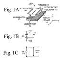
- Fig. 1 shows a conventional piezoelectric acceleration sensor 100.
- the acceleration sensor 100 includes a piezoelectric vibrator 102 and a circuit board 103.
- the piezoelectric vibrator 102 is provided on the circuit board 103.
- a weight 101 is provided on the piezoelectric vibrator 102.
- the piezoelectric vibrator 102 is polarized in Z direction in Fig. 1A.
- the weight 101 has a center of gravity outside the piezoelectric vibrator 102.
- the piezoelectric vibrator 102 referring to Fig. 1B, includes a capacitance Cd1 composed of electrodes 103a and 103b.
- Fig. 1C shows an equivalent circuit of the piezoelectric vibrator 102 shown in Fig. 1B.
- the generated electric charge Q1 on the piezoelectric vibrator 102 of the acceleration sensor 100 is detected as a voltage value or charge value, based on a voltage sensitivity SV (See an expression 1) dependent on the capacitance Cd1 or a charge sensitivity SQ (See an expression 2). It is thus detected that the vibration or shock has been applied.
- Japanese Patent Application Publication No. 2000-121661 discloses a charge-sensitive acceleration sensor 200.
- Fig. 2 shows the acceleration sensor 200 as a conventional technique 2.
- the acceleration sensor 200 includes a piezoelectric vibrator 202 having a double layer structure.
- Fig. 2B shows an equivalent circuit of the piezoelectric vibrator 202. With this configuration, sensing electrodes of a piezoelectric material are connected in parallel to adjust the polarized directions. The capacitance becomes larger and thus improves the detection sensitivity to the charge.
- the acceleration sensor that employs the layered piezoelectric material as described in the conventional technique 2
- the piezoelectric materials are multilayered, polarized axis of each piezoelectric material is adjusted, and the sensing electrodes are intricately connected. This results in problems, complicated configuration and complex manufacturing. These problems lead to another problem in cost reduction.
- the configuration of the conventional technique 2 the voltage sensitivity is lowered. This causes further another problem in that a detection signal is hard to be separated from the noises.
- the present invention has been made in view of the above-mentioned circumstances and provides an acceleration sensor with a simple configuration, while maintaining the voltage sensitivity and improving the charge sensitivity.
- the present invention includes, as claimed in claim 1, an acceleration sensor characterized by including a vibrator that generates an electric charge according to a stress, and a weight provided on the vibrator, the vibrator has multiple pairs of sensing electrodes on front and back surfaces, and capacitances formed with the sensing electrodes are connected in parallel. This makes it possible to connect the capacitances in parallel without a complicated structure. It is possible to realize the acceleration sensor having the improved charge sensitivity while maintaining the voltage sensitivity.
- Figs. 3A and 3B show a configuration of an acceleration sensor 10 in accordance with the present embodiment of the present invention.
- Fig. 3A is a cross-sectional view of the acceleration sensor 10.
- the acceleration sensor 10 includes a piezoelectric vibrator 2.
- the piezoelectric vibrator 2 is provided on a circuit board 3.
- a weight 1 is provided on the piezoelectric vibrator 2.
- the weight 1 has a center of gravity on a position deviated from an area above the piezoelectric vibrator 2.
- a front surface denotes the surface on which the weight of the piezoelectric vibrator 2 is provided
- a back surface denotes the surface on which the circuit board 3 is provided.
- sensing electrodes 3a and 3b, and 4a and 4b are provided on both front and back surfaces of the piezoelectric vibrator 2, as shown in Fig. 3B.
- the sensing electrodes 3a and 3b form a capacitance Cd1
- the sensing electrodes 4a and 4b form a capacitance Cd2.
- the sensing electrodes 3a and 4a are connected in parallel, and the sensing electrodes 3b and 4b are connected in parallel on the circuit board 3, as shown in Fig. 3B.
- the sensing electrodes facing aslant through the thickness of the piezoelectric vibrator 2 are connected in parallel (parallel connection electrode structure) among multiple sensing electrodes 3a, 3b, 4a, and 4b provided on the front and back surfaces of the piezoelectric vibrator 2, which is a single layer board.
- Fig. 3C shows an equivalent circuit of Fig. 3B.
- the capacitances Cd1 and Cd2 are connected in parallel, and a capacitance Cd of the whole piezoelectric vibrator 2 is expressed in the following (expression 3).
- the capacitance Cd of the present invention is twice as much as that of the piezoelectric vibrator 102 of the conventional technique 1.
- a generated charge Q is twice as much as the conventional technique 1, as shown in the following (expression 4). This is because a generated charge Q1 is detected on the capacitance Cd1, and a generated charge Q2 is detected on the capacitance Cd2.
- a voltage sensitivity SV' and a charge sensitivity SQ' of the acceleration sensor 10 are given by following (expression 5) and (expression 6).
- the acceleration sensor 10 in accordance with the present embodiment of the present invention has equal voltage sensitivity, and has the charge sensitivity twice as much as that of the conventional technique 2.
- Fig. 4 shows a comparison between the voltage sensitivity and charge sensitivity (actual measurement and calculation) of the present embodiment of the present invention and those (actual measurement and calculation) of the conventional technique 1.
- Figs. 5A through 5C show an example of connection between the sensing electrodes 3a, 3b, 4a, and 4b and the circuit board 3.
- the sensing electrodes 3b and 4a are provided on the surface (the back surface) directly in contact with the circuit board 3, and are connected to the circuit board 3 by directly bonding with metal bumps 7 and 8 made of gold, aluminum, or the like or conductive resin or anisotropic conductive resin, as shown in Fig. 5A.
- the sensing electrodes 3a and 4b provided on the front surface of the piezoelectric vibrator 2 are connected to the sensing electrodes 4a and 3b by bonding with metal wires 5 and 6 made of gold, aluminum, or the like, by way of grooves (cut portions 15 and 16) exposed after a sidewall of the weight 1 is removed.
- the configuration shown in Fig. 5B is thus obtained.
- the sensing electrodes 3a and 4a connected in parallel are connected to the sensing electrodes 3b and 4b connected in parallel.
- the parallel connection is realized between the sensing electrodes diagonally located through the piezoelectric vibrator 2.
- the acceleration sensor having improved charge sensitivity can be realized with a simple configuration, while maintaining the voltage sensitivity.
- Fig. 6 shows a connection structure of the sensing electrodes 3a, 3b, 4a, and 4b, in accordance with the present embodiment of the present invention.
- the sensing electrodes connected in parallel are connected by through holes 11 and 12 provided in a piezoelectric vibrator 2b.
- the sensing electrodes 3a and 4a, 4b and 3b which are arranged aslant through the piezoelectric vibrator 2b, are connected by the through holes 11 and 12 provided aslant in the direction of thickness in the piezoelectric vibrator 2b.
- the through holes 11 and 12 are crossed sterically not to interconnect inside the piezoelectric vibrator 2b.
- the through holes 11 and 12 are directly formed on the piezoelectric vibrator 2b by sandblasting.
- An interconnection which is not shown, is formed by filling or sputtering a conductive body such as gold, aluminum, or the like inside the through holes 11 and 12.
- a conductive body such as gold, aluminum, or the like inside the through holes 11 and 12.
- Figs. 7A and 7B show the configuration of the sensing electrodes and connection structure in accordance with the present embodiment of the present invention.
- the two capacitances Cd1 and Cd2 are equal, it is possible to change the shapes of the sensing electrodes (for example, 13a and 14b, or 23a and 24b) of the capacitances Cd1 and Cd2 in any way.
- the two pairs of the sensing electrodes 3a and 4a, and 3b and 4b are connected by metal wires 5 and 6.
- the metal wires 5 and 6 are replaced by conductive resin.
- Figs. 8A, 8B, and 8C are top views illustrating the connection structure of the present embodiment of the present invention.
- Fig. 8A shows a case where the connection shown in Fig. 5B is replaced by conductive resins 5a and 6a.
- Fig. 8B shows a case where the connection shown in Fig. 7A is replaced by the conductive resins 5a and 6a.
- Fig. 8C shows a case where the connection shown in Fig. 7B is replaced by the conductive resins 5a and 6a.
- an insulating material such as ceramics, glass, or the like is used for the weight 1.
- Other materials are employed in the present embodiment of the present invention.
- Fig. 9A is an example of a case where a metal material coated with the insulation material is employed in a weight 1a. It is possible to apply the same connection structure as the embodiments described above to the present embodiment of the present invention.
- Fig. 9B is an example of a case where a metal material that is not coated with the insulation material is employed in a weight 1b.
- an insulating layer (insulation layer) 9 is provided between the weight 1b and the piezoelectric vibrator 2. It is thus possible to avoid an electric connection between the sensing electrodes 3a and 4b provided on the front surface of the piezoelectric vibrator 2 and the weight 1b.
- the insulation layer 9 is formed with the use of epoxy resin or the like having an inorganic filler with a diameter of equal to or more than a surface roughness of the weight 1b and the piezoelectric vibrator 2.
- the sensing electrodes connected in parallel 3a and 4a, and 3b and 4b are connected by way of the cut portions 15 and 16, which are formed by removing the sidewall of the weight 1.
- the through holes are formed inside the weight 1 to obtain the same connection structure as the embodiments mentioned above.
- Fig. 10A is a cross-sectional view and a top view of a first example of the weight 1 and the connection structure in accordance with the present embodiment of the present invention.
- through holes 5b and 6b are formed inside the weight 1 to connect electrodes 13 and 14 provided on the weight 1 and the piezoelectric vibrator 2.
- the through holes 5b and 6b are crossed sterically to connect the electrodes located diagonally.
- the through holes 5b and 6b do not to interconnect inside the weight 1.
- the connection between the sensing electrodes 3a and 4a and the sensing electrodes 3b and 4b are achieved by connecting the electrodes 13 and 4a, and 14 and 3b.
- Fig. 10B is a cross-sectional view and a top view of a second example of the weight 1 and the connection structure in accordance with the present embodiment of the present invention.
- through holes 5c and 6c are formed inside the weight 1 to connect the electrodes 13 and 14 provided on the weight 1 and the piezoelectric vibrator 2.
- the through holes 5c and 6c are formed in a direction perpendicular to top and bottom faces of the weight 1 to connect the electrodes located on the top and bottom faces through the weight 1.
- Interconnections between the electrodes 13 and 14 provided on the top face of the weight 1 and the sensing electrodes 3b and 4a are crossed to be connected in parallel.
- the connection between the sensing electrodes 3a and 4a, and 3b and 4b are achieved by connecting the electrodes 13 and 4a, and the electrodes 14 and 3b.
- the metal wires 5 and 6 may be replaced by conductive resins 5b and 6b, for example, as shown in Fig. 10C.
- the acceleration sensor 10 in accordance with the embodiments of the present invention may be packaged with a lid 21 or the like to provide as an acceleration sensor package 20.
- the acceleration sensor that can enhance the charge sensitivity while maintaining the high voltage sensitivity, with a simple structure of the single-layered piezoelectric vibrator.
Landscapes
- Physics & Mathematics (AREA)
- General Physics & Mathematics (AREA)
- Pressure Sensors (AREA)
- Gyroscopes (AREA)
- Force Measurement Appropriate To Specific Purposes (AREA)
Applications Claiming Priority (3)
| Application Number | Priority Date | Filing Date | Title |
|---|---|---|---|
| JP2002237061A JP2004077255A (ja) | 2002-08-15 | 2002-08-15 | 加速度センサ |
| JP2002237061 | 2002-08-15 | ||
| PCT/JP2003/010348 WO2004017075A1 (fr) | 2002-08-15 | 2003-08-14 | Capteur d'acceleration |
Publications (2)
| Publication Number | Publication Date |
|---|---|
| EP1553418A1 true EP1553418A1 (fr) | 2005-07-13 |
| EP1553418A4 EP1553418A4 (fr) | 2009-03-11 |
Family
ID=31884431
Family Applications (1)
| Application Number | Title | Priority Date | Filing Date |
|---|---|---|---|
| EP03788112A Withdrawn EP1553418A4 (fr) | 2002-08-15 | 2003-08-14 | Capteur d'acceleration |
Country Status (7)
| Country | Link |
|---|---|
| US (1) | US7093489B2 (fr) |
| EP (1) | EP1553418A4 (fr) |
| JP (1) | JP2004077255A (fr) |
| KR (1) | KR100616385B1 (fr) |
| CN (1) | CN1675555A (fr) |
| TW (1) | TWI232937B (fr) |
| WO (1) | WO2004017075A1 (fr) |
Cited By (1)
| Publication number | Priority date | Publication date | Assignee | Title |
|---|---|---|---|---|
| EP2717059A4 (fr) * | 2011-05-26 | 2014-10-29 | Nec Corp | Capteur d'accélération |
Families Citing this family (7)
| Publication number | Priority date | Publication date | Assignee | Title |
|---|---|---|---|---|
| JP2004077255A (ja) | 2002-08-15 | 2004-03-11 | Fujitsu Media Device Kk | 加速度センサ |
| US20080072677A1 (en) * | 2006-09-26 | 2008-03-27 | Sorah Rhee | Bending mode accelerometer |
| US20080072671A1 (en) * | 2006-09-26 | 2008-03-27 | Eldon Eller | Leveraged shear mode accelerometers |
| US8833165B2 (en) * | 2009-02-17 | 2014-09-16 | Agency For Science, Technology And Research | Miniaturized piezoelectric accelerometers |
| CN102859369B (zh) * | 2010-02-02 | 2016-01-20 | Skf公司 | 加速度计中压力传感器的排列 |
| JP6123944B2 (ja) * | 2014-08-18 | 2017-05-10 | 株式会社村田製作所 | 圧電素子及び曲げ検出センサ |
| KR102023192B1 (ko) * | 2018-05-24 | 2019-11-04 | 이현주 | 지진감지모듈을 포함한 지진예보시스템 및 지진예보방법 |
Family Cites Families (12)
| Publication number | Priority date | Publication date | Assignee | Title |
|---|---|---|---|---|
| JPS63107215A (ja) * | 1986-10-23 | 1988-05-12 | Murata Mfg Co Ltd | 圧電振動部品 |
| EP0374870B1 (fr) * | 1988-12-23 | 1993-04-07 | Mitsubishi Denki Kabushiki Kaisha | Capteur d'accélération |
| JP3275459B2 (ja) | 1993-06-30 | 2002-04-15 | 松下電器産業株式会社 | 浴室ユニット |
| JPH0716168U (ja) * | 1993-08-27 | 1995-03-17 | 株式会社カンセイ | 圧電式加速度センサ |
| JP3373032B2 (ja) * | 1994-03-15 | 2003-02-04 | 富士通株式会社 | 加速度センサ |
| JP3333653B2 (ja) * | 1994-11-07 | 2002-10-15 | エフ・ディ−・ケイ株式会社 | 加速度センサ |
| CA2241929A1 (fr) * | 1996-10-29 | 1998-05-07 | Mitsui Chemicals, Incorporated | Gyroscope a vibrations |
| JP2001349900A (ja) * | 1999-12-28 | 2001-12-21 | Fujitsu Ltd | 加速度センサ及び加速度センサ装置 |
| JP2001228168A (ja) * | 2000-02-18 | 2001-08-24 | Fujitsu Ltd | 加速度センサ |
| JP2002156386A (ja) * | 2000-11-17 | 2002-05-31 | Fujitsu Ltd | 加速度センサ |
| JP2002296292A (ja) * | 2001-01-24 | 2002-10-09 | Fujitsu Ltd | 加速度センサ |
| JP2004077255A (ja) | 2002-08-15 | 2004-03-11 | Fujitsu Media Device Kk | 加速度センサ |
-
2002
- 2002-08-15 JP JP2002237061A patent/JP2004077255A/ja active Pending
-
2003
- 2003-08-14 WO PCT/JP2003/010348 patent/WO2004017075A1/fr not_active Ceased
- 2003-08-14 TW TW092122385A patent/TWI232937B/zh not_active IP Right Cessation
- 2003-08-14 CN CNA038193639A patent/CN1675555A/zh active Pending
- 2003-08-14 KR KR1020057002433A patent/KR100616385B1/ko not_active Expired - Fee Related
- 2003-08-14 EP EP03788112A patent/EP1553418A4/fr not_active Withdrawn
-
2005
- 2005-02-14 US US11/056,404 patent/US7093489B2/en not_active Expired - Fee Related
Cited By (1)
| Publication number | Priority date | Publication date | Assignee | Title |
|---|---|---|---|---|
| EP2717059A4 (fr) * | 2011-05-26 | 2014-10-29 | Nec Corp | Capteur d'accélération |
Also Published As
| Publication number | Publication date |
|---|---|
| TWI232937B (en) | 2005-05-21 |
| KR100616385B1 (ko) | 2006-08-28 |
| TW200403438A (en) | 2004-03-01 |
| CN1675555A (zh) | 2005-09-28 |
| EP1553418A4 (fr) | 2009-03-11 |
| US7093489B2 (en) | 2006-08-22 |
| JP2004077255A (ja) | 2004-03-11 |
| US20050172716A1 (en) | 2005-08-11 |
| WO2004017075A1 (fr) | 2004-02-26 |
| KR20050032602A (ko) | 2005-04-07 |
Similar Documents
| Publication | Publication Date | Title |
|---|---|---|
| JP3153860B2 (ja) | 衝撃荷重検出装置 | |
| JP4044919B2 (ja) | 3−ウェーハ構造を有するmems | |
| US6629462B2 (en) | Acceleration sensor, an acceleration detection apparatus, and a positioning device | |
| JP3401790B2 (ja) | 加速度センサ及びこの加速度センサを用いた加速度装置 | |
| US20040129079A1 (en) | Acceleration sensor | |
| US7296471B2 (en) | Acceleration sensor | |
| US5539270A (en) | Acceleration detector | |
| US7093489B2 (en) | Acceleration sensor | |
| JP2006275660A (ja) | 半導体センサおよびその製造方法 | |
| JP2005249454A (ja) | 容量型加速度センサ | |
| WO2003071287A1 (fr) | Capteur d'acceleration | |
| JP4261468B2 (ja) | 加速度センサ | |
| US7578184B2 (en) | Portable apparatus with an accelerometer device for free-fall detection | |
| JP2001027648A (ja) | 加速度センサ | |
| JP2004361394A (ja) | 容量型力学量センサ | |
| JP2002107374A (ja) | 加速度センサ及び加速度検出装置並びに位置決め装置 | |
| US20230349945A1 (en) | Inertial sensor and inertial measurement unit | |
| US20040187571A1 (en) | Capacitive-type semiconductor sensor | |
| JP2000171480A (ja) | 圧電センサ素子および加速度検出装置および加速度検出方法 | |
| CN103562731B (zh) | 加速度传感器 | |
| JP3342748B2 (ja) | 加速度センサ | |
| US20240118308A1 (en) | Physical Quantity Sensor And Inertial Measurement Device | |
| JP2008122304A (ja) | 静電容量式加速度センサ | |
| JP4706634B2 (ja) | 半導体センサおよびその製造方法 | |
| JPH09159690A (ja) | 加速度センサ |
Legal Events
| Date | Code | Title | Description |
|---|---|---|---|
| PUAI | Public reference made under article 153(3) epc to a published international application that has entered the european phase |
Free format text: ORIGINAL CODE: 0009012 |
|
| 17P | Request for examination filed |
Effective date: 20050309 |
|
| AK | Designated contracting states |
Kind code of ref document: A1 Designated state(s): AT BE BG CH CY CZ DE DK EE ES FI FR GB GR HU IE IT LI LU MC NL PT RO SE SI SK TR |
|
| RBV | Designated contracting states (corrected) |
Designated state(s): DE FR GB |
|
| A4 | Supplementary search report drawn up and despatched |
Effective date: 20090205 |
|
| STAA | Information on the status of an ep patent application or granted ep patent |
Free format text: STATUS: THE APPLICATION IS DEEMED TO BE WITHDRAWN |
|
| 18D | Application deemed to be withdrawn |
Effective date: 20090307 |