EP1553433B1 - Composant optique pour la transmission en parallèle de lumière à différentes longueurs d'ondes - Google Patents
Composant optique pour la transmission en parallèle de lumière à différentes longueurs d'ondes Download PDFInfo
- Publication number
- EP1553433B1 EP1553433B1 EP04019426A EP04019426A EP1553433B1 EP 1553433 B1 EP1553433 B1 EP 1553433B1 EP 04019426 A EP04019426 A EP 04019426A EP 04019426 A EP04019426 A EP 04019426A EP 1553433 B1 EP1553433 B1 EP 1553433B1
- Authority
- EP
- European Patent Office
- Prior art keywords
- array
- optical
- light signals
- demultiplexer
- multiplexer
- Prior art date
- Legal status (The legal status is an assumption and is not a legal conclusion. Google has not performed a legal analysis and makes no representation as to the accuracy of the status listed.)
- Expired - Lifetime
Links
Images


Classifications
-
- G—PHYSICS
- G02—OPTICS
- G02B—OPTICAL ELEMENTS, SYSTEMS OR APPARATUS
- G02B6/00—Light guides; Structural details of arrangements comprising light guides and other optical elements, e.g. couplings
- G02B6/24—Coupling light guides
- G02B6/26—Optical coupling means
- G02B6/28—Optical coupling means having data bus means, i.e. plural waveguides interconnected and providing an inherently bidirectional system by mixing and splitting signals
- G02B6/293—Optical coupling means having data bus means, i.e. plural waveguides interconnected and providing an inherently bidirectional system by mixing and splitting signals with wavelength selective means
- G02B6/29346—Optical coupling means having data bus means, i.e. plural waveguides interconnected and providing an inherently bidirectional system by mixing and splitting signals with wavelength selective means operating by wave or beam interference
- G02B6/29361—Interference filters, e.g. multilayer coatings, thin film filters, dichroic splitters or mirrors based on multilayers, WDM filters
- G02B6/29362—Serial cascade of filters or filtering operations, e.g. for a large number of channels
- G02B6/29365—Serial cascade of filters or filtering operations, e.g. for a large number of channels in a multireflection configuration, i.e. beam following a zigzag path between filters or filtering operations
- G02B6/29367—Zigzag path within a transparent optical block, e.g. filter deposited on an etalon, glass plate, wedge acting as a stable spacer
-
- G—PHYSICS
- G02—OPTICS
- G02B—OPTICAL ELEMENTS, SYSTEMS OR APPARATUS
- G02B6/00—Light guides; Structural details of arrangements comprising light guides and other optical elements, e.g. couplings
- G02B6/10—Light guides; Structural details of arrangements comprising light guides and other optical elements, e.g. couplings of the optical waveguide type
- G02B6/12—Light guides; Structural details of arrangements comprising light guides and other optical elements, e.g. couplings of the optical waveguide type of the integrated circuit kind
- G02B6/122—Basic optical elements, e.g. light-guiding paths
- G02B6/125—Bends, branchings or intersections
-
- G—PHYSICS
- G02—OPTICS
- G02B—OPTICAL ELEMENTS, SYSTEMS OR APPARATUS
- G02B6/00—Light guides; Structural details of arrangements comprising light guides and other optical elements, e.g. couplings
- G02B6/24—Coupling light guides
- G02B6/26—Optical coupling means
- G02B6/28—Optical coupling means having data bus means, i.e. plural waveguides interconnected and providing an inherently bidirectional system by mixing and splitting signals
- G02B6/2804—Optical coupling means having data bus means, i.e. plural waveguides interconnected and providing an inherently bidirectional system by mixing and splitting signals forming multipart couplers without wavelength selective elements, e.g. "T" couplers, star couplers
-
- G—PHYSICS
- G02—OPTICS
- G02B—OPTICAL ELEMENTS, SYSTEMS OR APPARATUS
- G02B6/00—Light guides; Structural details of arrangements comprising light guides and other optical elements, e.g. couplings
- G02B6/24—Coupling light guides
- G02B6/26—Optical coupling means
- G02B6/28—Optical coupling means having data bus means, i.e. plural waveguides interconnected and providing an inherently bidirectional system by mixing and splitting signals
- G02B6/293—Optical coupling means having data bus means, i.e. plural waveguides interconnected and providing an inherently bidirectional system by mixing and splitting signals with wavelength selective means
- G02B6/29379—Optical coupling means having data bus means, i.e. plural waveguides interconnected and providing an inherently bidirectional system by mixing and splitting signals with wavelength selective means characterised by the function or use of the complete device
- G02B6/2938—Optical coupling means having data bus means, i.e. plural waveguides interconnected and providing an inherently bidirectional system by mixing and splitting signals with wavelength selective means characterised by the function or use of the complete device for multiplexing or demultiplexing, i.e. combining or separating wavelengths, e.g. 1xN, NxM
-
- G—PHYSICS
- G02—OPTICS
- G02B—OPTICAL ELEMENTS, SYSTEMS OR APPARATUS
- G02B6/00—Light guides; Structural details of arrangements comprising light guides and other optical elements, e.g. couplings
- G02B6/24—Coupling light guides
- G02B6/42—Coupling light guides with opto-electronic elements
- G02B6/4201—Packages, e.g. shape, construction, internal or external details
- G02B6/4249—Packages, e.g. shape, construction, internal or external details comprising arrays of active devices and fibres
-
- G—PHYSICS
- G02—OPTICS
- G02B—OPTICAL ELEMENTS, SYSTEMS OR APPARATUS
- G02B6/00—Light guides; Structural details of arrangements comprising light guides and other optical elements, e.g. couplings
- G02B6/24—Coupling light guides
- G02B6/42—Coupling light guides with opto-electronic elements
- G02B6/4292—Coupling light guides with opto-electronic elements the light guide being disconnectable from the opto-electronic element, e.g. mutually self aligning arrangements
-
- G—PHYSICS
- G02—OPTICS
- G02B—OPTICAL ELEMENTS, SYSTEMS OR APPARATUS
- G02B6/00—Light guides; Structural details of arrangements comprising light guides and other optical elements, e.g. couplings
- G02B6/10—Light guides; Structural details of arrangements comprising light guides and other optical elements, e.g. couplings of the optical waveguide type
- G02B6/12—Light guides; Structural details of arrangements comprising light guides and other optical elements, e.g. couplings of the optical waveguide type of the integrated circuit kind
- G02B2006/12083—Constructional arrangements
- G02B2006/12104—Mirror; Reflectors or the like
-
- G—PHYSICS
- G02—OPTICS
- G02B—OPTICAL ELEMENTS, SYSTEMS OR APPARATUS
- G02B6/00—Light guides; Structural details of arrangements comprising light guides and other optical elements, e.g. couplings
- G02B6/24—Coupling light guides
- G02B6/26—Optical coupling means
- G02B6/28—Optical coupling means having data bus means, i.e. plural waveguides interconnected and providing an inherently bidirectional system by mixing and splitting signals
- G02B6/293—Optical coupling means having data bus means, i.e. plural waveguides interconnected and providing an inherently bidirectional system by mixing and splitting signals with wavelength selective means
- G02B6/29346—Optical coupling means having data bus means, i.e. plural waveguides interconnected and providing an inherently bidirectional system by mixing and splitting signals with wavelength selective means operating by wave or beam interference
- G02B6/29361—Interference filters, e.g. multilayer coatings, thin film filters, dichroic splitters or mirrors based on multilayers, WDM filters
- G02B6/2937—In line lens-filtering-lens devices, i.e. elements arranged along a line and mountable in a cylindrical package for compactness, e.g. 3- port device with GRIN lenses sandwiching a single filter operating at normal incidence in a tubular package
-
- G—PHYSICS
- G02—OPTICS
- G02B—OPTICAL ELEMENTS, SYSTEMS OR APPARATUS
- G02B6/00—Light guides; Structural details of arrangements comprising light guides and other optical elements, e.g. couplings
- G02B6/24—Coupling light guides
- G02B6/42—Coupling light guides with opto-electronic elements
- G02B6/4201—Packages, e.g. shape, construction, internal or external details
- G02B6/4204—Packages, e.g. shape, construction, internal or external details the coupling comprising intermediate optical elements, e.g. lenses, holograms
- G02B6/4206—Optical features
-
- G—PHYSICS
- G02—OPTICS
- G02B—OPTICAL ELEMENTS, SYSTEMS OR APPARATUS
- G02B6/00—Light guides; Structural details of arrangements comprising light guides and other optical elements, e.g. couplings
- G02B6/24—Coupling light guides
- G02B6/42—Coupling light guides with opto-electronic elements
- G02B6/4201—Packages, e.g. shape, construction, internal or external details
- G02B6/4204—Packages, e.g. shape, construction, internal or external details the coupling comprising intermediate optical elements, e.g. lenses, holograms
- G02B6/4214—Packages, e.g. shape, construction, internal or external details the coupling comprising intermediate optical elements, e.g. lenses, holograms the intermediate optical element having redirecting reflective means, e.g. mirrors, prisms for deflecting the radiation from horizontal to down- or upward direction toward a device
-
- G—PHYSICS
- G02—OPTICS
- G02B—OPTICAL ELEMENTS, SYSTEMS OR APPARATUS
- G02B6/00—Light guides; Structural details of arrangements comprising light guides and other optical elements, e.g. couplings
- G02B6/24—Coupling light guides
- G02B6/42—Coupling light guides with opto-electronic elements
- G02B6/4201—Packages, e.g. shape, construction, internal or external details
- G02B6/4248—Feed-through connections for the hermetical passage of fibres through a package wall
Definitions
- the present invention relates to an apparatus and method for multiplexing light signals for transmission, or for receiving and demultiplexing light signals.
- Parallel Optics and Wavelength Division Multiplexing are two optical communications techniques that enable increased bandwidth density in communications systems.
- multiple optical data signals are transmitted along a multi-fiber ribbon, with a single optical signal being transmitted in each fiber.
- WDM multiple optical data signals are combined and transmitted along a single optical fiber, with each optical signal being carried on a different wavelength.
- PWDM Parallel WDM
- the two techniques are combined by transmitting multiple optical wavelengths through each fiber of a parallel fiber ribbon.
- US 2003/0152113 A1 discloses an optoelectronic assembly having a first interface member, a second interface member and a multiplexing member disposed therebetween.
- the first interface member On its side opposing the multiplexing member, the first interface member has a receptacle for a support member, in which there is constructed an optical path that is formed by an optical waveguide.
- An array chip with a plurality of optoelectronic transducers is assigned to the second interface member.
- the array chip is disposed on a substrate.
- US 6,385,374 B2 relates to multichannel transmission or reception operation via a plurality of separate optical waveguides in wavelength division multiplex operation.
- a multichannel assembly is disclosed having a first chip which is a transducer array and a drive circuit for driving the transducer array.
- the transducer array and the drive circuit are disposed on a support board in direct proximity.
- a multiwavelength transmitter module comprises an optical bench on which is mounted four vertical cavity surface emitting laser (VCSEL) die arrays and an interconnect chip with interconnect wires.
- VCSEL vertical cavity surface emitting laser
- WO 03/079087 A1 discloses an optical module, the base of which consists of an image guide which has embedded therein optical fibers. Opto-electronic devices are flip-chiped onto the image guide within the module.
- Embodiments in accordance with the invention provide for parallel multiwavelength transmission and reception of light signals.
- the apparatus and method include an array of diodes mounted on a circuit for receiving electrical signals from the circuit and converting them into an array of corresponding light signals, for receiving an array of a plurality of light signals and converting them into corresponding electrical signals.
- An optical multiplexer or demultiplexer located adjacent the array of diodes, receives the array of light signals and converts them into a set of corresponding parallel multiplexed light signals, or receives a set of parallel multiplexed light signals and converts them into the array of the plurality of light signals.
- Embodiments in accordance with the invention provide for a parallel multiwavelength optical subassembly (PMOSA).
- PMOSA parallel multiwavelength optical subassembly
- Embodiments can include either a transmitter (Tx) or receiver (Rx) subassembly that enables a PWDM solution to be extremely compact and low cost.
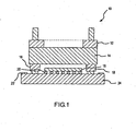
- FIG. 1 is a side view of an exemplary PWDM apparatus 10 for this subassembly in order to multiplex light signals for transmission, or to receive and demultiplex light signals.
- the side view of FIG. 1 shows only one "slice" (cross-section) of the apparatus, and implementations include arrays of components, as further described below.
- FIG. 2 is a perspective exploded view of the exemplary apparatus 10.
- Light signals can include any type of optical data signal.
- apparatus 10 includes a parallel Tx or Rx integrated circuit (IC) 24, and such ICs are known in the art.
- IC 24 includes bond pads 22 for electrical communication with the circuitry within it.
- Vertical Cavity Surface Emitting Lasers (VCSELs) or PIN photodiode arrays 16 sit on top of IC 24 and solder balls 20, providing electrical communication between the circuitry in IC 24 and arrays 16.
- the photodiodes can also be implemented with, for example, MSM photodiodes or any other type of photodetector.
- the optical sources can also be implemented with, for example, any laser that can emit light perpendicular to the IC, or an edge-emitting laser with a turning mirror.
- certain embodiments do not necessarily require an IC and can instead use another electronic sub-mount such as a piece of silicon, Gallium arsenide, or Indium phosphide with electrical traces.
- PWDM multiplexer or demultiplexer optics 14 are positioned over arrays 16 and held in place by a spacer 18 positioned between optics 14 and IC 24.
- spacer 18 can provide for an hermetic seal between optics 14 and IC 24 by being composed of an hermetic material and surrounding the enclosed space between optics 14 and IC 24.
- a lid 12 includes alignment pins in order to align optics 14 with an optical transmission medium such as a parallel fiber ribbon.
- a fiber ribbon connector to accomplish this alignment is the MT ferrule connector.
- any type of mechanical features can be used to connect optics 14 with a fiber ribbon or other parallel terminations for transmitting light signals.
- the apparatus 10 can be manufactured as a chip-mounted enclosure, an example of which is described in U.S. Patent No. 6,351,027 , incorporated herein by reference.
- the embodiment shown in FIGS. 1 and 2 can include, for example, two types of implementations, hermetic and non-hermetic embodiments.
- the PMOSA is a chip-mounted enclosure.
- the PMOSA comprises IC 24 (a multichannel Tx or Rx circuit), the VCSEL or photodiode arrays 16 flip-chip mounted on top of the IC 24, a wall (spacer 18 composed of metal or silicon, for example) for hermetic encapsulation, the optical component 14 (implemented in a material impervious to moisture), for combining or separating wavelengths and coupling between the fibers and the optoelectronic components, and the mechanical lid 12 for aligning the optical signals to a fiber ribbon via the alignment pins.
- the ICs, wall, optics, and lid are fabricated as wafers of components that align to each other, then the alignment and assembly of these components can be accomplished on a wafer scale, dramatically reducing the cost of the PMOSA.
- the wall (spacer 18 bonded and forming a barrier between optical element 14 and IC 24) in this hermetic embodiment can be composed of, for example, silicon, metal, ceramic, or glass.
- the lid may be composed of any of those materials for the wall, for example.
- the multiplexer and demultiplexer in this hermetic embodiment can be composed of, for example, glass, Gallium arsenide, Gallium Phosphide, silicon, Indium Phosphide, or any hermetic material optically transparent at the wavelengths of the VCSELs.
- the PMOSA is not necessarily hermetically sealed.
- the PMOSA includes IC 24 (a multichannel Tx or Rx circuit), the VCSEL or photodiode arrays 16 flip-chip mounted on top of the IC 24, and a molded plastic optical component 14 for combining or separating the optical wavelengths and coupling between the fibers and the optoelectronic components.
- This plastic component may also include mechanical features for aligning the optical signals to a fiber ribbon, via the alignment pins, and for attaching the plastic component to the IC 24 (spacer 18 composed of plastic, for example).
- the wall (spacer 18) in this non-hermetic embodiment can be composed of, for example, plastic, silicon, metal, ceramic, or glass.
- the lid may be composed of any of those materials for the wall, for example.
- the multiplexer and demultiplexer in this non-hermetic embodiment can be composed of, for example, plastic, glass, Gallium arsenide, Gallium phosphate, a semiconductor, silicon, Indium, or any possibly non-hermetic material optically transparent at the wavelengths of the VCSELs.
- the optical component used in a PMOSA can belong to one of two general families, for example: zigzag and splitter/combiner.
- zigzag optical multiplexers and demultiplexers light of different wavelengths is combined or separated through successive bounces on dielectric interference filters, which transmit one wavelength and reflect other wavelengths.
- the optics function to either split a single input optical beam into multiple equal output beams, or to combine multiple input optical beams into a single output optical beam.
- a combiner such a device is typically wavelength insensitive.
- the wavelength insensitive optics will be combined with wavelength filters associated with each detector to transmit only the desired wavelength.
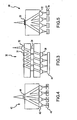
- FIG. 3 is a diagram illustrating an optical zigzag multiplexer or demultiplexer 30 as one implementation of optics 14.
- light filters 34 are positioned between refractive optical element (ROE) asphere lens arrays 32 (1 x 12 array) and 38 (4 x 12 array).
- the filters 34 filter light at particular wavelengths to demultiplex light signals from lens array 32 through successive bounces of the light signals off asphere mirrors 31 (3 x 12 array) and through filters 34, and to provide the demultiplexed light signals to a PIN array 40 (4 x 12 array corresponding with array 16 in FIG. 1 ).
- the filters 34 can multiplex light signals from array 40 and provide the multiplexed light signals to lens arrays 32.
- ROE asphere lenses 38 focus the light signals onto PIN array 40 for demultiplexing, or can receive light signals from VCSEL array 40 for multiplexing.
- lens array 38 is integrated into the substrate-side of the PIN photodiode array 40, rather than being integrated into the demultiplexer. This configuration reduces the overall PMOSA complexity and improves the alignment tolerance of the demultiplexer relative to the photodiode array.
- FIG. 4 is a diagram illustrating an optical combiner multiplexer 42 as one implementation of optics 14 for a Tx embodiment of apparatus 10.
- multiplexer 42 VCSEL arrays 46 (4 - 1 x 12 arrays corresponding with array 16 in FIG. 1 ) provide light signals to ROE asphere lens arrays 43 (4 x 12 array), which focus the individual light signals onto lens arrays 44 (12 - 2 x 2 arrays) to be optically combined for transmission via a fiber optic ribbon aligned with the optics using the alignment pins on lid 12.
- FIG. 5 is a diagram illustrating an optical splitter demultiplexer 48 as one implementation of optics 14 for a Rx embodiment of apparatus 10.
- an optical splitter array 50 (1 x 12 array) receives multiplexed light signals from the fiber ribbon, aligned with the optics via the alignment pins on lid 12, and it transmits the light signals to ROE asphere lens arrays 52 (4 x 12 array), which then focuses the demultiplexed light signals onto PIN arrays 54 (4 - 1 x 12 arrays corresponding with array 16 in FIG. 1 ).
- Each of PIN arrays 54 includes a wavelength filter 51 that allows a desired wavelength to pass, while blocking undesired wavelengths of light.
- FIGS. 3-5 illustrate the numbers identifying the sizes of the various arrays in FIGS. 3-5 are provided for illustrative purposes only for these exemplary embodiments. Other embodiments can include arrays of different sizes. For example, other embodiments in accordance with the invention can use 4, 6, or 8 wavelengths and fiber ribbons having 4, 12, 24, or 48 fibers. Also, any number of wavelengths and signals can be used in particular implementations, as well as with a variety of materials such as the examples provided above. Moreover, each of the FIGS. 3-5 illustrates only one input/output in a side view for the multiplexers and demultiplexers.
- FIG. 6 is a diagram illustrating the three-dimensional embodiment of an optical demultiplexer, zigzag slab 30 with attached wavelength filters 34, aligned to a lensed photodiode array.
- lenses 32 function as input lenses
- array 40 functions as a detector array.
- FIG. 7 is a diagram illustrating the three-dimensional embodiment of an optical multiplexer, zigzag slab 30 with attached wavelength filters 34 and attached lens array 38, aligned to a VCSEL array.
- lenses 32 function as output lenses
- array 40 functions as the VCSEL arrays.
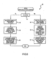
- FIG. 8 is a flow chart of a method 60 for processing optical signals in accordance with the invention using, for example, the apparatus described above.
- Method 60 determines whether a transmission (Tx) routine or reception routine (Rx) is to be executed (step 61).
- Tx transmission
- Rx reception routine
- an array of electrical signals is received (step 62) and converted into an array of light signals (step 64).
- the array of light signals are then converted into parallel multiplexed light signals for transmission (step 66).
- parallel multiplexed light signals are received (step 68) and converted into an array of demultiplexed light signals (step 70).
- the array of light signals are then converted into an array of electrical signals for reception by an IC or other component (step 72).
- Other steps may also be incorporated into method 60 depending upon a particular implementation.
- Embodiments in accordance with the invention can be used for a variety of applications as an optical interconnect product. For example, they can be used for ultra-short reach transmission of signals for chip-to-chip, board-to-board, or rack-to-rack (in-room) transmission of high volumes of data. They can also be used for high speed transmission (for example, 100 gigabits/second) of high volumes of data between processors in multi-processor systems or between large routers in networking systems. As yet another example, they can be used as optical backplanes and high-speed board-to-board interconnects in systems. Other applications are also possible, depending upon particular implementations.
Landscapes
- Physics & Mathematics (AREA)
- General Physics & Mathematics (AREA)
- Optics & Photonics (AREA)
- Engineering & Computer Science (AREA)
- Microelectronics & Electronic Packaging (AREA)
- Optical Couplings Of Light Guides (AREA)
Claims (8)
- Appareil permettant de fournir une émission à longueur d'ondes multiples en parallèle de signaux optiques, comprenant :un réseau de sources optiques (16) pour recevoir des signaux électriques et convertir les signaux électriques en un réseau de signaux lumineux correspondants ; etun multiplexeur optique (14), situé de manière adjacente au réseau de sources optiques (16), pour recevoir le réseau de signaux lumineux et convertir le réseau de signaux lumineux en un ensemble de signaux lumineux multiplexés en parallèle correspondants ;le multiplexeur (14) étant positionné sur le réseau de sources optiques (16) ;un couvercle (12) monté sur le multiplexeur optique (14) et procurant un alignement du multiplexeur optique (14) sur un support d'émission optique pour émettre les signaux lumineux multiplexés en parallèle ;caractérisé en ce qu'il comporteun circuit intégré (24) ;une pièce d'espacement (18) entourant le réseau de sources optiques (16) et montée entre le circuit intégré (24) et le multiplexeur optique (14) ;l'appareil comprenant le réseau de sources optiques (16) pour recevoir les signaux électriques en provenance du circuit intégré (24) ;le multiplexeur (14) comprenant un premier réseau (44) de lentilles et un second réseau de lentilles sous la forme d'un réseau (43) de lentilles asphériques qui concentre les signaux lumineux individuels en provenance des sources optiques (46) sur le premier réseau (44) de lentilles pour être combiné optiquement pour une émission via un ruban à fibre optique aligné sur les éléments optiques utilisant le couvercle (12) ;le circuit intégré (24), la pièce d'espacement (18), le multiplexeur (14) et le couvercle (12) étant fabriqués comme des plaquettes de composants qui sont alignées les unes par rapport aux autres, l'alignement et l'assemblage de ces composants étant réalisés à l'échelle d'une plaquette.
- Appareil selon la revendication 1, dans lequel la pièce d'espacement (18) et le multiplexeur optique (14) sont composés d'un matériau hermétique.
- Appareil selon la revendication 1, dans lequel la pièce d'espacement (18) et le multiplexeur optique (14) sont composés d'un matériau non-hermétique.
- Appareil de réception d'une émission à longueur d'ondes multiples en parallèle de signaux optiques, comprenant :un réseau de photodétecteurs (16) pour recevoir un réseau d'une pluralité de signaux lumineux et convertir le réseau de signaux lumineux en un réseau de signaux électriques correspondant ; etun démultiplexeur optique (14), situé de manière adjacente au réseau de photodétecteurs (16), pour recevoir un ensemble de signaux lumineux multiplexés en parallèle et convertir l'ensemble de signaux lumineux multiplexés en parallèle dans le réseau de la pluralité de signaux lumineuxle démultiplexeur (14) étant positionné sur le réseau de photodétecteurs (16) ;un couvercle (12) monté sur le démultiplexeur optique (14) et procurant un alignement du démultiplexeur optique (14) sur un support d'émission optique pour recevoir les signaux lumineux multiplexés en parallèle ;caractérisé en ce qu'il comporteun circuit intégré (24) ;une pièce d'espacement (18) entourant le réseau de photodétecteurs (16) et montée entre le circuit intégré (24) et le démultiplexeur optique (14) ;le démultiplexeur comprenant un réseau (52) de lentilles asphériques et un réseau (50) de séparateur optique pour recevoir les signaux lumineux multiplexés en parallèle en provenance du ruban de fibre avec les éléments optiques via le couvercle (12), et pour émettre les signaux lumineux au réseau (52) de lentilles asphériques, le réseau (52) de lentilles asphériques concentrant les signaux lumineux démultiplexés sur le réseau de photodétecteurs dont chaque photodétecteur comporte une fibre de longueur d'onde ;le circuit intégré (24), la pièce d'espacement (18), le démultiplexeur (14) et le couvercle (12) étant fabriqués comme des plaquettes de composants qui s'alignent les unes sur les autres, l'alignement et l'assemblage de ces composants étant réalisés à l'échelle d'une plaquette.
- Appareil selon la revendication 4 dans lequel la pièce d'espacement (18) et le démultiplexeur optique (14) sont composés d'un matériau hermétique.
- Appareil selon la revendication 4 dans lequel la pièce d'espacement (18) et le démultiplexeur optique (14) sont composés d'un matériau non-hermétique.
- Appareil selon l'une des revendications 4 à 6 dans lequel le réseau de photodétecteurs est un réseau de diodes (16).
- Appareil selon l'une des revendications 1 à 3, dans lequel le réseau de sources optiques est un réseau de diodes (16).
Applications Claiming Priority (2)
| Application Number | Priority Date | Filing Date | Title |
|---|---|---|---|
| US10/754,131 US6937786B2 (en) | 2004-01-09 | 2004-01-09 | Parallel multiwavelength optical subassembly |
| US754131 | 2004-01-09 |
Publications (2)
| Publication Number | Publication Date |
|---|---|
| EP1553433A1 EP1553433A1 (fr) | 2005-07-13 |
| EP1553433B1 true EP1553433B1 (fr) | 2009-08-05 |
Family
ID=34592593
Family Applications (1)
| Application Number | Title | Priority Date | Filing Date |
|---|---|---|---|
| EP04019426A Expired - Lifetime EP1553433B1 (fr) | 2004-01-09 | 2004-08-16 | Composant optique pour la transmission en parallèle de lumière à différentes longueurs d'ondes |
Country Status (3)
| Country | Link |
|---|---|
| US (1) | US6937786B2 (fr) |
| EP (1) | EP1553433B1 (fr) |
| DE (1) | DE602004022383D1 (fr) |
Families Citing this family (30)
| Publication number | Priority date | Publication date | Assignee | Title |
|---|---|---|---|---|
| TWI247152B (en) * | 2004-12-24 | 2006-01-11 | Ind Tech Res Inst | Array type optical sub-device |
| US20060291858A1 (en) * | 2005-01-31 | 2006-12-28 | Lou Xin S | Bi-directional compound-WDM fiberoptic system architecture with redundancy protection for transmission of data, voice and video signals |
| KR100810312B1 (ko) * | 2006-02-07 | 2008-03-04 | 삼성전자주식회사 | 다중 채널 방식의 양방향 광 송수신기 |
| EP1818701A1 (fr) * | 2006-02-09 | 2007-08-15 | BAE Systems PLC | Interface optoélectronique |
| US8737837B2 (en) * | 2008-10-14 | 2014-05-27 | Corning Cable Systems Llc | Multi-level distributed fiber optic architectures |
| US8873967B2 (en) * | 2008-10-17 | 2014-10-28 | Corning Cable Systems Llc | Optical interconnection modules for hybrid electrical-optical networks |
| US9482840B2 (en) * | 2009-05-27 | 2016-11-01 | Corning Cable Systems Llc | Port mapping for series connected fiber optic terminals |
| US8009959B2 (en) * | 2009-06-17 | 2011-08-30 | Corning Cable Systems Llc | Optical interconnection methods for high-speed data-rate optical transport systems |
| US8251591B2 (en) | 2009-06-17 | 2012-08-28 | Corning Cable Systems | Optical interconnection assemblies and systems for high-speed data-rate optical transport systems |
| CN102460255A (zh) * | 2009-06-17 | 2012-05-16 | 康宁光缆系统有限责任公司 | 用于高速数据率传输系统的光学互连 |
| EP2312352B1 (fr) * | 2009-09-07 | 2018-04-18 | Electronics and Telecommunications Research Institute | Modules de réception et de transmission optique à plusieurs longueurs d'onde |
| US20110206379A1 (en) * | 2010-02-25 | 2011-08-25 | International Business Machines Corporation | Opto-electronic module with improved low power, high speed electrical signal integrity |
| US9097873B2 (en) | 2010-04-14 | 2015-08-04 | Corning Cable Systems Llc | Port mapping in fiber optic network devices |
| US8406587B2 (en) | 2010-05-06 | 2013-03-26 | Commscope, Inc. Of North Carolina | Quad small form factor pluggable (QSFP) adapter module |
| US9057863B2 (en) | 2012-07-25 | 2015-06-16 | Corning Cable Systems Llc | Polarity scheme for parallel-optics data transmission |
| US9097874B2 (en) | 2012-07-25 | 2015-08-04 | Corning Optical Communications LLC | Polarity configurations for parallel optics data transmission, and related apparatuses, components, systems, and methods |
| CN102890313B (zh) * | 2012-10-22 | 2015-07-15 | 索尔思光电(成都)有限公司 | Cwdm多工/解多工器系统及其制造方法 |
| CN104007519A (zh) * | 2013-02-27 | 2014-08-27 | 鸿富锦精密工业(深圳)有限公司 | 光通讯模组 |
| US10007065B2 (en) * | 2013-10-31 | 2018-06-26 | Hewlett Packard Enterprise Development Lp | Multiplexed optoelectronic engines |
| US9442259B2 (en) * | 2013-11-11 | 2016-09-13 | Sumitomo Electric Industries, Ltd. | Method for producing optical assembly and optical assembly |
| US9419718B2 (en) * | 2014-08-18 | 2016-08-16 | Cisco Technology, Inc. | Aligning optical components in a multichannel receiver or transmitter platform |
| WO2016164035A1 (fr) | 2015-04-10 | 2016-10-13 | Hewlett Packard Enterprise Development Lp | Filtres surmoulés |
| US10359572B2 (en) * | 2016-10-31 | 2019-07-23 | Electronics And Telecommunications Research Institute | Device and method for detecting optical signal |
| US10551569B2 (en) * | 2017-02-02 | 2020-02-04 | Alliance Fiber Optic Products, Inc. | Wavelength-division multiplexing optical assembly with multiple collimator sets |
| WO2019152612A1 (fr) | 2018-02-05 | 2019-08-08 | Inneos, Llc | Coupleur optique multicanal |
| US20190278036A1 (en) * | 2018-03-07 | 2019-09-12 | Lightwave Logic Inc. | Embedded hermetic capsule and method |
| CN111936914B (zh) * | 2018-04-05 | 2022-03-11 | 三菱电机株式会社 | 光合分波器及其制造方法 |
| US10788633B2 (en) * | 2018-04-30 | 2020-09-29 | Hewlett Packard Enterprise Development Lp | Complementary reverse order filters |
| TWM573438U (zh) * | 2018-10-25 | 2019-01-21 | 聯鈞光電股份有限公司 | 波長分波多工模組 |
| WO2020197532A1 (fr) * | 2019-03-22 | 2020-10-01 | Source Photonics, Inc. | Système et procédé de transfert de signaux optiques dans des dispositifs photoniques et procédé de fabrication du système |
Citations (4)
| Publication number | Priority date | Publication date | Assignee | Title |
|---|---|---|---|---|
| US6267515B1 (en) * | 1998-02-27 | 2001-07-31 | Oki Electric Industry Co., Ltd. | Optical coupling module and manufacturing method of the same |
| US6419404B1 (en) * | 1999-07-01 | 2002-07-16 | The Regents Of The University Of California | Compact multiwavelength transmitter module for multimode fiber optic ribbon cable |
| US6563976B1 (en) * | 2000-05-09 | 2003-05-13 | Blaze Network Products, Inc. | Cost-effective wavelength division multiplexer and demultiplexer |
| WO2003079087A1 (fr) * | 2002-03-14 | 2003-09-25 | Nurlogic Design, Inc. | Module optique et procede de fabrication associe |
Family Cites Families (11)
| Publication number | Priority date | Publication date | Assignee | Title |
|---|---|---|---|---|
| US4755017A (en) | 1984-11-29 | 1988-07-05 | Kaptron, Inc. | Construction for fiber optics communications modules using elements bonded along abutting flat surfaces and method of fabricating same |
| US5894535A (en) | 1997-05-07 | 1999-04-13 | Hewlett-Packard Company | Optical waveguide device for wavelength demultiplexing and waveguide crossing |
| US6117699A (en) | 1998-04-10 | 2000-09-12 | Hewlett-Packard Company | Monolithic multiple wavelength VCSEL array |
| US6198864B1 (en) | 1998-11-24 | 2001-03-06 | Agilent Technologies, Inc. | Optical wavelength demultiplexer |
| US6385374B2 (en) * | 1999-01-06 | 2002-05-07 | Infineon Technologies Ag | Multichannel electro-optical assembly |
| US6201908B1 (en) * | 1999-07-02 | 2001-03-13 | Blaze Network Products, Inc. | Optical wavelength division multiplexer/demultiplexer having preformed passively aligned optics |
| US6341023B1 (en) | 1999-07-23 | 2002-01-22 | Tycom (Us) Inc. | Multiple level modulation in a wavelength-division multiplexing (WDM) systems |
| US6282337B1 (en) | 1999-09-24 | 2001-08-28 | Radiant Photonics, Inc. | System and method for wavelength division multiplexing and demultiplexing |
| US6351027B1 (en) | 2000-02-29 | 2002-02-26 | Agilent Technologies, Inc. | Chip-mounted enclosure |
| DE10043324A1 (de) * | 2000-08-23 | 2002-03-14 | Infineon Technologies Ag | Opto-elektronische Baugruppe zum Multiplexen und/oder Demultiplexen optischer Signale |
| US6539142B2 (en) | 2001-06-01 | 2003-03-25 | Agilent Technologies, Inc. | System and method for actively aligning mirrors in an optical switch |
-
2004
- 2004-01-09 US US10/754,131 patent/US6937786B2/en not_active Expired - Fee Related
- 2004-08-16 EP EP04019426A patent/EP1553433B1/fr not_active Expired - Lifetime
- 2004-08-16 DE DE602004022383T patent/DE602004022383D1/de not_active Expired - Lifetime
Patent Citations (4)
| Publication number | Priority date | Publication date | Assignee | Title |
|---|---|---|---|---|
| US6267515B1 (en) * | 1998-02-27 | 2001-07-31 | Oki Electric Industry Co., Ltd. | Optical coupling module and manufacturing method of the same |
| US6419404B1 (en) * | 1999-07-01 | 2002-07-16 | The Regents Of The University Of California | Compact multiwavelength transmitter module for multimode fiber optic ribbon cable |
| US6563976B1 (en) * | 2000-05-09 | 2003-05-13 | Blaze Network Products, Inc. | Cost-effective wavelength division multiplexer and demultiplexer |
| WO2003079087A1 (fr) * | 2002-03-14 | 2003-09-25 | Nurlogic Design, Inc. | Module optique et procede de fabrication associe |
Also Published As
| Publication number | Publication date |
|---|---|
| US20050152640A1 (en) | 2005-07-14 |
| EP1553433A1 (fr) | 2005-07-13 |
| US6937786B2 (en) | 2005-08-30 |
| DE602004022383D1 (de) | 2009-09-17 |
Similar Documents
| Publication | Publication Date | Title |
|---|---|---|
| EP1553433B1 (fr) | Composant optique pour la transmission en parallèle de lumière à différentes longueurs d'ondes | |
| US10466433B2 (en) | Optical module including silicon photonics chip and coupler chip | |
| KR100921566B1 (ko) | 모듈식 광 트랜시버 | |
| US20080226228A1 (en) | Optical system connection structure, optical component, and optical communication module | |
| USRE45214E1 (en) | Integrated transceiver with lightpipe coupler | |
| KR101584923B1 (ko) | 멀티채널 송수신기 | |
| US20020114587A1 (en) | Apparatus for coupling a fiber optic cable to an optoelectronic device, a system including the apparatus, and a method of forming the same | |
| US6960031B2 (en) | Apparatus and method of packaging two dimensional photonic array devices | |
| US12259587B2 (en) | Optical connector for photonic circuits | |
| EP1780565B1 (fr) | Dispositif micro-optique avec guide d'alignement en U | |
| KR20220106722A (ko) | 초소형 광송신 모듈 | |
| JP2017194565A (ja) | 光通信モジュール及びその製造方法 | |
| KR20200066736A (ko) | 광 트랜시버를 위한 광학 패키징 및 설계 | |
| US7412148B2 (en) | Optical module including an optical component and an optical device | |
| US20070133928A1 (en) | Canted-fiber duplex optical assembly | |
| CN115343808B (zh) | 光模块装置 | |
| US20090032984A1 (en) | Method for manufacturing an optical fiber with filter and method for batch manufacturing optical fibers with filter | |
| EP3757639A1 (fr) | Interposeur | |
| US7177506B2 (en) | Method for forming an aligned optical sub-assembly | |
| Althaus et al. | Microsystems and wafer processes for volume production of highly reliable fiber optic components for telecom-and datacom-application | |
| CN115343809A (zh) | 光发射装置与光接收装置 | |
| CN115343801A (zh) | 光发射装置与光接收装置 | |
| KR101769034B1 (ko) | 광학 엔진 | |
| US20260118611A1 (en) | Multi-channel laser-to-external modulator array coupling enabled co-packaged optics | |
| JP7609257B2 (ja) | 光接続構造、パッケージ構造および光モジュール |
Legal Events
| Date | Code | Title | Description |
|---|---|---|---|
| PUAI | Public reference made under article 153(3) epc to a published international application that has entered the european phase |
Free format text: ORIGINAL CODE: 0009012 |
|
| AK | Designated contracting states |
Kind code of ref document: A1 Designated state(s): AT BE BG CH CY CZ DE DK EE ES FI FR GB GR HU IE IT LI LU MC NL PL PT RO SE SI SK TR |
|
| AX | Request for extension of the european patent |
Extension state: AL HR LT LV MK |
|
| 17P | Request for examination filed |
Effective date: 20051118 |
|
| AKX | Designation fees paid |
Designated state(s): DE FR GB |
|
| 17Q | First examination report despatched |
Effective date: 20051229 |
|
| RAP1 | Party data changed (applicant data changed or rights of an application transferred) |
Owner name: AVAGO TECHNOLOGIES FIBER IP (SINGAPORE) PTE. LTD. |
|
| GRAP | Despatch of communication of intention to grant a patent |
Free format text: ORIGINAL CODE: EPIDOSNIGR1 |
|
| GRAS | Grant fee paid |
Free format text: ORIGINAL CODE: EPIDOSNIGR3 |
|
| GRAA | (expected) grant |
Free format text: ORIGINAL CODE: 0009210 |
|
| AK | Designated contracting states |
Kind code of ref document: B1 Designated state(s): DE FR GB |
|
| REG | Reference to a national code |
Ref country code: GB Ref legal event code: FG4D |
|
| REF | Corresponds to: |
Ref document number: 602004022383 Country of ref document: DE Date of ref document: 20090917 Kind code of ref document: P |
|
| PLBE | No opposition filed within time limit |
Free format text: ORIGINAL CODE: 0009261 |
|
| STAA | Information on the status of an ep patent application or granted ep patent |
Free format text: STATUS: NO OPPOSITION FILED WITHIN TIME LIMIT |
|
| 26N | No opposition filed |
Effective date: 20100507 |
|
| GBPC | Gb: european patent ceased through non-payment of renewal fee |
Effective date: 20091105 |
|
| PG25 | Lapsed in a contracting state [announced via postgrant information from national office to epo] |
Ref country code: GB Free format text: LAPSE BECAUSE OF NON-PAYMENT OF DUE FEES Effective date: 20091105 |
|
| REG | Reference to a national code |
Ref country code: FR Ref legal event code: ST Effective date: 20110502 |
|
| PG25 | Lapsed in a contracting state [announced via postgrant information from national office to epo] |
Ref country code: FR Free format text: LAPSE BECAUSE OF NON-PAYMENT OF DUE FEES Effective date: 20091005 |
|
| REG | Reference to a national code |
Ref country code: DE Ref legal event code: R081 Ref document number: 602004022383 Country of ref document: DE Owner name: AVAGO TECHNOLOGIES GENERAL IP (SINGAPORE) PTE., SG Free format text: FORMER OWNER: AVAGO TECHNOLOGIES FIBER IP (SINGAPORE) PTE. LTD., SINGAPORE, SG Effective date: 20130725 Ref country code: DE Ref legal event code: R082 Ref document number: 602004022383 Country of ref document: DE Representative=s name: DILG HAEUSLER SCHINDELMANN PATENTANWALTSGESELL, DE Effective date: 20130725 |
|
| PGFP | Annual fee paid to national office [announced via postgrant information from national office to epo] |
Ref country code: DE Payment date: 20150722 Year of fee payment: 12 |
|
| REG | Reference to a national code |
Ref country code: DE Ref legal event code: R119 Ref document number: 602004022383 Country of ref document: DE |
|
| PG25 | Lapsed in a contracting state [announced via postgrant information from national office to epo] |
Ref country code: DE Free format text: LAPSE BECAUSE OF NON-PAYMENT OF DUE FEES Effective date: 20170301 |