EP1553569A1 - Optisches aufzeichnungsmedium und auszeichnungseinrichtung - Google Patents
Optisches aufzeichnungsmedium und auszeichnungseinrichtung Download PDFInfo
- Publication number
- EP1553569A1 EP1553569A1 EP03788012A EP03788012A EP1553569A1 EP 1553569 A1 EP1553569 A1 EP 1553569A1 EP 03788012 A EP03788012 A EP 03788012A EP 03788012 A EP03788012 A EP 03788012A EP 1553569 A1 EP1553569 A1 EP 1553569A1
- Authority
- EP
- European Patent Office
- Prior art keywords
- data
- linking
- regions
- recording
- pseudo
- Prior art date
- Legal status (The legal status is an assumption and is not a legal conclusion. Google has not performed a legal analysis and makes no representation as to the accuracy of the status listed.)
- Withdrawn
Links
Images




Classifications
-
- G—PHYSICS
- G11—INFORMATION STORAGE
- G11B—INFORMATION STORAGE BASED ON RELATIVE MOVEMENT BETWEEN RECORD CARRIER AND TRANSDUCER
- G11B20/00—Signal processing not specific to the method of recording or reproducing; Circuits therefor
- G11B20/10—Digital recording or reproducing
- G11B20/12—Formatting, e.g. arrangement of data block or words on the record carriers
-
- G—PHYSICS
- G11—INFORMATION STORAGE
- G11B—INFORMATION STORAGE BASED ON RELATIVE MOVEMENT BETWEEN RECORD CARRIER AND TRANSDUCER
- G11B20/00—Signal processing not specific to the method of recording or reproducing; Circuits therefor
- G11B20/10—Digital recording or reproducing
- G11B20/12—Formatting, e.g. arrangement of data block or words on the record carriers
- G11B20/1217—Formatting, e.g. arrangement of data block or words on the record carriers on discs
-
- G—PHYSICS
- G11—INFORMATION STORAGE
- G11B—INFORMATION STORAGE BASED ON RELATIVE MOVEMENT BETWEEN RECORD CARRIER AND TRANSDUCER
- G11B20/00—Signal processing not specific to the method of recording or reproducing; Circuits therefor
- G11B20/10—Digital recording or reproducing
- G11B20/14—Digital recording or reproducing using self-clocking codes
-
- G—PHYSICS
- G11—INFORMATION STORAGE
- G11B—INFORMATION STORAGE BASED ON RELATIVE MOVEMENT BETWEEN RECORD CARRIER AND TRANSDUCER
- G11B7/00—Recording or reproducing by optical means, e.g. recording using a thermal beam of optical radiation by modifying optical properties or the physical structure, reproducing using an optical beam at lower power by sensing optical properties; Record carriers therefor
-
- G—PHYSICS
- G11—INFORMATION STORAGE
- G11B—INFORMATION STORAGE BASED ON RELATIVE MOVEMENT BETWEEN RECORD CARRIER AND TRANSDUCER
- G11B7/00—Recording or reproducing by optical means, e.g. recording using a thermal beam of optical radiation by modifying optical properties or the physical structure, reproducing using an optical beam at lower power by sensing optical properties; Record carriers therefor
- G11B7/007—Arrangement of the information on the record carrier, e.g. form of tracks, actual track shape, e.g. wobbled, or cross-section, e.g. v-shaped; Sequential information structures, e.g. sectoring or header formats within a track
-
- G—PHYSICS
- G11—INFORMATION STORAGE
- G11B—INFORMATION STORAGE BASED ON RELATIVE MOVEMENT BETWEEN RECORD CARRIER AND TRANSDUCER
- G11B20/00—Signal processing not specific to the method of recording or reproducing; Circuits therefor
- G11B20/10—Digital recording or reproducing
- G11B20/12—Formatting, e.g. arrangement of data block or words on the record carriers
- G11B2020/1264—Formatting, e.g. arrangement of data block or words on the record carriers wherein the formatting concerns a specific kind of data
- G11B2020/1265—Control data, system data or management information, i.e. data used to access or process user data
- G11B2020/1277—Control data, system data or management information, i.e. data used to access or process user data for managing gaps between two recordings, e.g. control data in linking areas, run-in or run-out fields, guard or buffer zones
-
- G—PHYSICS
- G11—INFORMATION STORAGE
- G11B—INFORMATION STORAGE BASED ON RELATIVE MOVEMENT BETWEEN RECORD CARRIER AND TRANSDUCER
- G11B20/00—Signal processing not specific to the method of recording or reproducing; Circuits therefor
- G11B20/10—Digital recording or reproducing
- G11B20/12—Formatting, e.g. arrangement of data block or words on the record carriers
- G11B2020/1264—Formatting, e.g. arrangement of data block or words on the record carriers wherein the formatting concerns a specific kind of data
- G11B2020/1265—Control data, system data or management information, i.e. data used to access or process user data
- G11B2020/1287—Synchronisation pattern, e.g. VCO fields
-
- G—PHYSICS
- G11—INFORMATION STORAGE
- G11B—INFORMATION STORAGE BASED ON RELATIVE MOVEMENT BETWEEN RECORD CARRIER AND TRANSDUCER
- G11B2220/00—Record carriers by type
- G11B2220/20—Disc-shaped record carriers
- G11B2220/21—Disc-shaped record carriers characterised in that the disc is of read-only, rewritable, or recordable type
- G11B2220/215—Recordable discs
- G11B2220/216—Rewritable discs
-
- G—PHYSICS
- G11—INFORMATION STORAGE
- G11B—INFORMATION STORAGE BASED ON RELATIVE MOVEMENT BETWEEN RECORD CARRIER AND TRANSDUCER
- G11B2220/00—Record carriers by type
- G11B2220/20—Disc-shaped record carriers
- G11B2220/21—Disc-shaped record carriers characterised in that the disc is of read-only, rewritable, or recordable type
- G11B2220/215—Recordable discs
- G11B2220/218—Write-once discs
-
- G—PHYSICS
- G11—INFORMATION STORAGE
- G11B—INFORMATION STORAGE BASED ON RELATIVE MOVEMENT BETWEEN RECORD CARRIER AND TRANSDUCER
- G11B2220/00—Record carriers by type
- G11B2220/20—Disc-shaped record carriers
- G11B2220/25—Disc-shaped record carriers characterised in that the disc is based on a specific recording technology
- G11B2220/2537—Optical discs
- G11B2220/2562—DVDs [digital versatile discs]; Digital video discs; MMCDs; HDCDs
Definitions
- the present invention relates to an optical recording medium and to a recording apparatus for forming the recording medium.
- a linking region is formed at that junction portion. Synchronization data for reading the information data written into a data region, which follows the linking region, is written into the linking region.
- linking regions are formed on such a recordable recording medium leads to a problem that there is a possibility of incompatibility in the recording format with read-only recording media such as DVD-ROMs that are not recordable.
- An optical recording medium having recorded data on a track thereof comprises on the track: a plurality of data block regions each of which includes main data of a block which serves as an error correction unit for the main data and which is divided into a predetermined number of main data pieces, each of which has data for identifying the main data; and linking regions each of which has pseudo data and is inserted between the plurality of data block regions; wherein when the linking regions on the track are adjacent, recording patterns of the pseudo data of the adjacent linking regions are different from each other.
- a recording apparatus for recording data onto a track of an optical recording medium comprises: a main data recording means for forming on the track a plurality of data block regions each of which includes main data of a block which serves as an error correction unit for the main data and which is divided into a predetermined number of main data pieces, each of which has data for identifying the main data; and a linking data recording means for inserting linking regions each of which has pseudo data between the plurality of data block regions onto the track; wherein the linking data recording means, when the linking regions on the track are adjacent, forms the pseudo data of the adjacent linking regions with recording patterns which are different from each other.
- a recording method for recording data onto a track of an optical recording medium comprises the steps of: forming on the track a plurality of data block regions each of which includes main data of a block which serves as an error correction unit for the main data and which is divided into a predetermined number of main data pieces, each of which has data for identifying the main data; and inserting linking regions each of which has pseudo data between the plurality of data block regions onto the track; wherein when the linking regions on the track are adjacent, the pseudo data of the adjacent linking regions is formed with recording patterns which are different from each other.
- Fig. 1 shows an original disk recording apparatus according to the present invention.
- the recording apparatus records information onto an original recording disk 1 for DVD-ROMs, and includes a master clock generator 11, a PLL circuit 12, a recording signal generation circuit 13, an optical modulator 14, a recording actuator 15, a spindle motor 16, a servo controller 17, and a main controller 18.
- the master clock generator 11 generates a master clock signal, and supplies the master clock signal to the PLL circuit 12 and the servo controller 17.
- the servo controller 17 is supplied with the master clock signal, and with a frequency signal FG indicating a rotation frequency from the spindle motor 16.
- the servo controller 17 carries out rotation control for the spindle motor 16 such that the frequency signal FG is synchronized with the master clock signal, that is, it carries out spindle servo control.
- the PLL circuit 12 generates a recording clock signal based on the master clock signal.
- the recording signal generation circuit 13 includes a data generation portion 20, an ECC block generation circuit 21, a random value generator 22, a timing circuit 23, a switching circuit 24, a modulator 25, and a synchronization adding circuit 26.
- the data generation portion 20 outputs information data (main data) to be recorded and address data corresponding to the information data.
- the ECC block generation circuit 21 outputs sector data adopted to ECC (error correction code) blocks based on the information data and the address data.
- the random value generator 22 generates random data for linking regions.
- the timing circuit 23 generates a timing signal for each ECC block in response to the recording clock signal.
- the switching circuit 24 selectively outputs one of information data in the ECC block and the random data in accordance with the timing signal.
- the modulator 25 performs 8-16 modulation for data output from the switching circuit 24.
- the synchronization adding circuit 26 adds a synchronization code having a 14T synchronization pattern to the modulated data so as to output a recording signal.
- the main controller 18 controls the components 20 to 26 inside the recording signal generation circuit 13 in synchronization with the output clock of the PLL circuit 12.
- the optical modulator 14 modulates laser light in accordance with the recording signal output from the recording signal generation circuit 13, and supplies the modulated laser light to a recording actuator 15.
- the recording actuator 15 irradiates the laser light onto the recording portion of the original recording disk 1 rotated by the spindle motor 16, thus carrying out exposure.
- the random value generator 22 includes a memory 31, eleven D flip-flop circuits 32 to 42, and one adder 44.
- An initial value of eleven bits is previously stored in the memory 31, and each one bit is supplied to the D flip-flops circuits 32 to 42 in response to a command from the main controller 18 at the beginning of recording of the original recording disk 1.
- Each of the D flip-flops circuits 32 to 42 has a preset input, and the bits corresponding to the initial value is respectively supplied to those preset inputs from the memory 31.
- each of the D flip-flops circuits 32 to 42 outputs from the output Q one bit of data supplied to the input D.
- the D flip-flops circuits 32 to 42 are connected in the form of a ring via the adder 44.
- the adder 44 is connected between the flip-flop circuits 32 and 33, and the output Q of the flip-flop circuit 42 is connected to the adder 44 and to the input D of the flip-flop circuit 32.
- the adder 44 adds data of the output Q of the flip-flop circuit 32 and data of the output Q of the flip-flop circuit 42, and supplies a result of the addition to the input D of the flip-flop circuit 33.
- Data having eight bits for the linking region is output from the outputs Q of the D flip-flop circuits 35 to 42.
- the linking region data is pseudo data of an information data piece.
- the ECC block generation circuit 21 Based on information data and address data to be recorded, the ECC block generation circuit 21 successively produces and outputs a data pieces of 91 bytes.
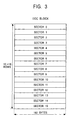
- one ECC block has sixteen sectors, as shown in Fig. 3.
- Each sector has a data structure of 13 rows 182 bytes. 91 bytes of each row constitute one data piece, so that each row has two data pieces (91 bytes
- the data pieces are supplied via the switching circuit 24 to the modulator 25. After having been subjected to 8-16 modulation, the data pieces are supplied to the synchronization adding circuit 26.
- the synchronization adding circuit 26 adds a synchronization code (32 bits) including a 14T synchronization pattern to the data pieces having 182 bytes (1456 bits) that have been modulated, to generate a recording signal.
- the synchronization code is one of eight codes SY0 to SY7, and serves as identification data for identifying data position in each sector.
- Fig. 4 illustrates the data structure of the recording signal for one sector.
- the synchronization code (SY0 to SY7) is located before the modulated data pieces, and two pairs of synchronization code and data piece are arranged in each row.
- the initial value is output from the memory 31 to the eleven D flip-flop circuits 32 to 42 in the random value generator 22.
- Each of the D flip-flop circuits 32 to 42 outputs a corresponding bit value of the initial value.
- the output values of the D flip-flop circuits 35 to 42 then serve as the linking region data.
- each of the D flip-flop circuits 32 to 42 read the output value of each of the D flip-flop circuits or the adder 44 connected to each input side, and the D flip-flop circuits 35 to 42 output as eight bits (one byte) of linking region data.
- the linking region data is pseudo data of the above-described data pieces, and consists of 91 bytes. For one linking region,
- the switching circuit 24 performs a switching operation in response to the timing signal after relaying the data pieces for one ECC block portion from the ECC block generation circuit 21. Thus, the switching circuit 24 becomes a state in which the output data from the random value generator 22 is relayed to the modulator 25.
- the linking region data is supplied from the random value generator 22 via the switching circuit 24 to the modulator 25. After being subjected to 8-16 modulation, the linking region data is supplied to the synchronization adding circuit 26.
- the synchronization adding circuit 26 adds a linking region synchronization code (32 bits) including a 14T synchronization pattern to the linking region data of 182 bytes (1456 bits) that have been modulated, to generate a recording signal.
- the first synchronization code of one row is SYX
- the second synchronization code is SYY.
- Each of the synchronization codes SYX and SYY has a pattern that is different from the synchronization codes SY0 to SY7, and represents a linking region.
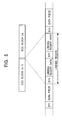
- the linking region is formed between ECC blocks (data block regions), and as shown in Fig. 5, includes two synchronization are arranged between one ECC block (n next ECC block (n).
- the recording signal output from the recording signal generation circuit 13 modulates laser light in the optical modulator 14, and after the modulation, the laser light is supplied to the recording actuator 15.
- the recording actuator 15 irradiates the laser light onto the recording portion of the original recording disk 1, which is rotated by the spindle motor 16, and thus exposure is performed.
- optical disks are obtained by duplication with a stamper of the master disk.
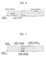
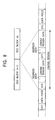
- Linking regions are formed on each track portion of the optical disk, as shown in Fig. 6 for example. Furthermore, between any adjacent track portions, the linking regions may be formed adjacently to one another, as shown in Fig. 7. However, since the random value generated from the random value generator 22 is used for the linking region data as described above, the data patterns of the linking region of the adjacent track portions are different from one another. For example, in the data patterns of adjacent linking regions shown in Fig. 7, the first pattern, the second pattern and the third pattern are mutually different.
- a tracking control for controlling a reading light beam on a recording track.
- the phase-difference method can be used as the tracking control for high-density optical disks such as DVD-ROMs.
- a tracking error signal is generated, which indicates the error between the irradiation position of the light beam and the recording track, in accordance with the difference between the sum signals of the light-receiving signals of opposite light-receiving portions in a photo-detector partitioned into four partitions.
- the tracking error signal when the correlation between adjacent track portions is strong, then the tracking error signal includes cross-talk components from the adjacent track portions, so that the tracking control becomes instable. If there are adjacent linking regions in adjacent track portions, the data pattern of those linking regions are different from one another, so that the correlation of the adjacent track portions can be reduced. Thus, it is possible to attain a stable tracking control even when using the phase-difference method for the tracking control.
- the random value generator 22 uses current address data (which indicates an address of the adjacent data region) as the initial value. That is to say, as indicated by a dashed line in Fig. 1, address data may be supplied to the random value generator 22, and the address data may be input from the preset input into the D flip-flop circuits 32 to 42 when the first linking region has been reached, to generate the linking region data. Furthermore, it is also possible to prepare a plurality of initial values in the memory 31, and to select one of the plurality of initial values in accordance with the address data.
- the address data may also be recorded together with the random linking region data in the random value generator 22.
- the synchronization codes SYX and SYY, the address data and the linking region data are arranged in that order in the two synchronization frames of the linking region. If the random value generation pattern of the random value generator 22 corresponding to the initial value is previously known, then it is possible to read out the address data and the linking region data, and to use the linking region data as useful data, based on the relation between the address data and the linking region data.
- the scrambling circuit 29 consists of an EX-OR circuit. Scrambling data of eight bits is previously written into the memory 30. In the scrambling circuit 29, the EX-OR value of the scrambling data and the linking region data generated by the random value generator 22 for each linking region is obtained, and that value is used as the final linking region data.
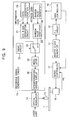
- Fig. 10 shows another configuration example of a recording signal generation circuit 13.
- the random value generator 22 in series with a random value generator 28, as in the configuration shown in Fig. 9.
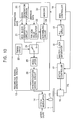
- Fig. 11 shows another configuration example of a recording signal generation circuit 13.
- the ECC block generation circuit 21, the modulator 25, the synchronization adding circuit 26 and the switching circuit 24 are connected in that order, and the switching circuit 24 is provided in the stage following the synchronization adding circuit 26.
- the random value generator 22 and a modulator 22a are provided as a configuration for generating linking region data. After the linking region data output from the random value generator 22 have been subjected to 8-16 modulation by the modulator 22a, the data is supplied to the switching circuit 24.
- the switching circuit 24 selectively supplies either the output data of the synchronization adding circuit 26 or the output data of the modulator 22a to the optical modulator 14.
- no synchronization code is added to the linking region data, so that the linking region formed between the ECC blocks on the track of the disk 1 has only linking region data that is pseudo data not including the synchronization code.
- linking data recording means forms the pseudo data of the adjacent linking regions with recording patterns which are different from each other.
- the recording patterns of pseudo data of linking regions that are located on adjacent track portions of a track are different from one another.
Landscapes
- Engineering & Computer Science (AREA)
- Signal Processing (AREA)
- Optical Recording Or Reproduction (AREA)
- Signal Processing For Digital Recording And Reproducing (AREA)
Applications Claiming Priority (5)
| Application Number | Priority Date | Filing Date | Title |
|---|---|---|---|
| JP2002234476 | 2002-08-12 | ||
| JP2002234476 | 2002-08-12 | ||
| JP2003019159 | 2003-01-28 | ||
| JP2003019159A JP3889365B2 (ja) | 2002-08-12 | 2003-01-28 | 光学式記録媒体、記録装置、記録方法及び光学式記録媒体の製造方法 |
| PCT/JP2003/009300 WO2004017310A1 (ja) | 2002-08-12 | 2003-07-23 | 光学式記録媒体及び記録装置 |
Publications (2)
| Publication Number | Publication Date |
|---|---|
| EP1553569A1 true EP1553569A1 (de) | 2005-07-13 |
| EP1553569A4 EP1553569A4 (de) | 2006-06-21 |
Family
ID=31497659
Family Applications (1)
| Application Number | Title | Priority Date | Filing Date |
|---|---|---|---|
| EP03788012A Withdrawn EP1553569A4 (de) | 2002-08-12 | 2003-07-23 | Optisches aufzeichnungsmedium und auszeichnungseinrichtung |
Country Status (12)
| Country | Link |
|---|---|
| US (2) | US7313069B2 (de) |
| EP (1) | EP1553569A4 (de) |
| JP (1) | JP3889365B2 (de) |
| KR (1) | KR100898956B1 (de) |
| CN (1) | CN100343910C (de) |
| AU (1) | AU2003252233B2 (de) |
| BR (1) | BR0313447A (de) |
| CA (1) | CA2494552C (de) |
| MX (1) | MXPA05001600A (de) |
| MY (1) | MY135320A (de) |
| TW (2) | TWI284315B (de) |
| WO (1) | WO2004017310A1 (de) |
Cited By (2)
| Publication number | Priority date | Publication date | Assignee | Title |
|---|---|---|---|---|
| EP1429331A3 (de) * | 2002-12-13 | 2008-08-13 | Sony Corporation | Nur-Wiedergabe Aufzeichungsmedium, Wiedergabegerät, Wiedergabeverfahren und Plattenherstellungsverfahren |
| EP1529286A4 (de) * | 2002-08-17 | 2009-11-11 | Lg Electronics Inc | Dichter optischer datenträger, verfahren zum aufzeichnen von adressen- und/oder servoinformationen auf dem dichten optischen datenträger und verfahren zur wiedergabe von auf dem dichten optischen datenträger aufgezeichneten daten |
Families Citing this family (5)
| Publication number | Priority date | Publication date | Assignee | Title |
|---|---|---|---|---|
| EP1571664A3 (de) * | 2002-06-05 | 2010-03-24 | Lg Electronics Inc. | Struktur eines Verknüpfungsbereichs, die auf einem hochdichten Nur-Lese-Aufzeichnungsmedium ausgebildet wird, und Herstellungs-/Reproduktionsverfahren und -Vorrichtung dafür |
| JP2004253099A (ja) * | 2003-02-21 | 2004-09-09 | Toshiba Corp | シンクフレーム構造、情報記憶媒体、情報記録方法、情報再生方法、および情報再生装置 |
| CN101312349B (zh) * | 2007-05-26 | 2010-08-25 | 华为技术有限公司 | 信息块编码及同步检测的方法和装置 |
| US8009531B2 (en) * | 2009-10-01 | 2011-08-30 | Mediatek Inc. | Methods for overwite cycle improvement of optical storage medium and related machine readable media |
| US8856198B2 (en) * | 2012-03-30 | 2014-10-07 | Freescale Semiconductor, Inc. | Random value production methods and systems |
Family Cites Families (31)
| Publication number | Priority date | Publication date | Assignee | Title |
|---|---|---|---|---|
| JPS61220134A (ja) * | 1985-03-27 | 1986-09-30 | Hitachi Ltd | 光デイスク |
| JP3158474B2 (ja) * | 1991-03-28 | 2001-04-23 | ソニー株式会社 | 記録方法、ディスク記録装置及びディスク再生装置 |
| JP3158557B2 (ja) | 1991-09-27 | 2001-04-23 | ソニー株式会社 | 再生装置 |
| JP3440952B2 (ja) * | 1993-02-24 | 2003-08-25 | ソニー株式会社 | データ記録方法及びデータ再生方法 |
| US5949750A (en) * | 1993-11-30 | 1999-09-07 | Victor Company Of Japan, Ltd. | Method and apparatus for recording an information signal with scrambling thereof |
| JP2723832B2 (ja) | 1994-06-07 | 1998-03-09 | 松下電器産業株式会社 | 光学式情報記録担体及び光学式情報記録方法、ならびにそれらを利用した光学式情報再生装置 |
| DE69507080T2 (de) * | 1994-06-07 | 1999-05-27 | Matsushita Electric Industrial Co., Ltd., Kadoma, Osaka | Optisches Informationsaufzeichnungsmedium, optisches Informationsaufzeichnungsverfahren, und optisches Informationswiedergabegerät hierfür |
| CN1106640C (zh) * | 1994-08-25 | 2003-04-23 | 索尼公司 | 光盘和光盘驱动装置 |
| CA2192062C (en) | 1995-04-04 | 2002-10-29 | Shin-Ichi Tanaka | Recording medium, recording method and apparatus, and reproduction method and apparatus |
| AU1454697A (en) * | 1996-02-16 | 1997-09-02 | Philips Electronics N.V. | Device for recording an information carrier, method and information carrier therefor |
| CN1288639C (zh) * | 1996-04-11 | 2006-12-06 | 松下电器产业株式会社 | 光盘 |
| JP3845849B2 (ja) * | 1996-10-18 | 2006-11-15 | ソニー株式会社 | 記録装置および記録方法、並びに記録媒体 |
| EP1271490B1 (de) | 1996-10-23 | 2011-12-21 | Panasonic Corporation | Optische Platte |
| JP2868744B2 (ja) | 1997-04-09 | 1999-03-10 | 株式会社東芝 | データ記録方法、記録装置、再生装置及び再生方法 |
| JP4144054B2 (ja) * | 1997-07-24 | 2008-09-03 | ソニー株式会社 | 光ディスクの記録方法 |
| JP3814966B2 (ja) * | 1997-08-14 | 2006-08-30 | ソニー株式会社 | 記録媒体、データ伝送装置、データ受信装置及び光ディスク装置 |
| JPH11176095A (ja) * | 1997-12-05 | 1999-07-02 | Sony Corp | データ記録装置及びデータ記録方法 |
| JPH11232797A (ja) | 1998-02-18 | 1999-08-27 | Hitachi Ltd | ディスク再生装置および再生方法 |
| AU1559900A (en) * | 1998-12-09 | 2000-06-26 | Koninklijke Philips Electronics N.V. | Method and device for recording information in units |
| EP1045391A1 (de) * | 1999-04-16 | 2000-10-18 | Koninklijke Philips Electronics N.V. | Verfahren und Vorrichtung zur Informationsaufzeichnung in Einheiten |
| US6842411B2 (en) | 1999-12-22 | 2005-01-11 | Lg Electronics, Inc. | Optical disc driver and data recording method therefor |
| JP3513088B2 (ja) * | 2000-07-28 | 2004-03-31 | 株式会社東芝 | 読出し専用型光ディスク |
| JP4103323B2 (ja) * | 2000-10-27 | 2008-06-18 | 日本ビクター株式会社 | 情報信号記録方法、情報信号記録装置及び記録媒体 |
| JP2002150698A (ja) * | 2000-11-06 | 2002-05-24 | Pioneer Electronic Corp | 情報記録方法、情報記録装置、情報再生方法及び情報再生装置 |
| JP2002170333A (ja) * | 2000-11-28 | 2002-06-14 | Pioneer Electronic Corp | 情報記録方法、情報記録装置、情報再生方法及び情報再生装置 |
| KR100713094B1 (ko) * | 2000-12-26 | 2007-05-02 | 파이오니아 가부시키가이샤 | 정보 기록 매체, 및 정보 재생 장치 및 방법 |
| US6985426B2 (en) | 2001-02-23 | 2006-01-10 | Matsushita Electric Industrial Co., Ltd. | Method and apparatus for recording optical information including dummy data, and optical disk having such data recorded thereon |
| US7512052B2 (en) * | 2001-03-16 | 2009-03-31 | Ricoh Company, Ltd. | Formatting of phase-change optical disc for improved signal characteristics |
| JP4202658B2 (ja) * | 2002-02-22 | 2008-12-24 | 富士通マイクロエレクトロニクス株式会社 | データ書き込み装置及びdvdフォーマットデータ生成方法 |
| EP1571664A3 (de) * | 2002-06-05 | 2010-03-24 | Lg Electronics Inc. | Struktur eines Verknüpfungsbereichs, die auf einem hochdichten Nur-Lese-Aufzeichnungsmedium ausgebildet wird, und Herstellungs-/Reproduktionsverfahren und -Vorrichtung dafür |
| JP4337341B2 (ja) * | 2002-12-13 | 2009-09-30 | ソニー株式会社 | 再生専用記録媒体、再生装置、再生方法、ディスク製造方法 |
-
2003
- 2003-01-28 JP JP2003019159A patent/JP3889365B2/ja not_active Expired - Lifetime
- 2003-07-23 BR BR0313447-4A patent/BR0313447A/pt not_active Application Discontinuation
- 2003-07-23 CA CA2494552A patent/CA2494552C/en not_active Expired - Lifetime
- 2003-07-23 EP EP03788012A patent/EP1553569A4/de not_active Withdrawn
- 2003-07-23 AU AU2003252233A patent/AU2003252233B2/en not_active Expired
- 2003-07-23 MX MXPA05001600A patent/MXPA05001600A/es active IP Right Grant
- 2003-07-23 KR KR1020057002166A patent/KR100898956B1/ko not_active Expired - Fee Related
- 2003-07-23 WO PCT/JP2003/009300 patent/WO2004017310A1/ja not_active Ceased
- 2003-07-23 CN CNB038191806A patent/CN100343910C/zh not_active Expired - Lifetime
- 2003-08-07 TW TW092121683A patent/TWI284315B/zh not_active IP Right Cessation
- 2003-08-07 TW TW094107524A patent/TWI326449B/zh not_active IP Right Cessation
- 2003-08-08 US US10/636,709 patent/US7313069B2/en not_active Expired - Lifetime
- 2003-08-11 MY MYPI20033041A patent/MY135320A/en unknown
-
2007
- 2007-11-09 US US11/979,893 patent/US7545721B2/en not_active Expired - Lifetime
Cited By (3)
| Publication number | Priority date | Publication date | Assignee | Title |
|---|---|---|---|---|
| EP1529286A4 (de) * | 2002-08-17 | 2009-11-11 | Lg Electronics Inc | Dichter optischer datenträger, verfahren zum aufzeichnen von adressen- und/oder servoinformationen auf dem dichten optischen datenträger und verfahren zur wiedergabe von auf dem dichten optischen datenträger aufgezeichneten daten |
| EP1429331A3 (de) * | 2002-12-13 | 2008-08-13 | Sony Corporation | Nur-Wiedergabe Aufzeichungsmedium, Wiedergabegerät, Wiedergabeverfahren und Plattenherstellungsverfahren |
| US8320225B2 (en) | 2002-12-13 | 2012-11-27 | Sony Corporation | Reproduction-only recording medium, reproducing apparatus, reproducing method, and disk manufacturing method |
Also Published As
| Publication number | Publication date |
|---|---|
| CN1675691A (zh) | 2005-09-28 |
| US20040027957A1 (en) | 2004-02-12 |
| TW200405277A (en) | 2004-04-01 |
| MY135320A (en) | 2008-03-31 |
| AU2003252233A1 (en) | 2004-03-03 |
| JP2004134049A (ja) | 2004-04-30 |
| US20080137523A1 (en) | 2008-06-12 |
| JP3889365B2 (ja) | 2007-03-07 |
| US7545721B2 (en) | 2009-06-09 |
| BR0313447A (pt) | 2005-07-12 |
| TW200521986A (en) | 2005-07-01 |
| MXPA05001600A (es) | 2005-04-25 |
| KR20050056958A (ko) | 2005-06-16 |
| CA2494552A1 (en) | 2004-02-26 |
| TWI326449B (en) | 2010-06-21 |
| CN100343910C (zh) | 2007-10-17 |
| KR100898956B1 (ko) | 2009-05-25 |
| US7313069B2 (en) | 2007-12-25 |
| WO2004017310A1 (ja) | 2004-02-26 |
| AU2003252233B2 (en) | 2008-09-11 |
| TWI284315B (en) | 2007-07-21 |
| CA2494552C (en) | 2011-05-10 |
| EP1553569A4 (de) | 2006-06-21 |
Similar Documents
| Publication | Publication Date | Title |
|---|---|---|
| KR100713097B1 (ko) | 정보 기록 매체, 및 정보 재생 장치 및 방법 | |
| US7545721B2 (en) | Optical recording medium and recording apparatus, the medium including a linking region between unit block regions | |
| KR101039561B1 (ko) | 광 디스크 매체, 데이터 기록 방법 및 장치 | |
| CN1662985B (zh) | 使用光记录介质的信息处理装置和数据记录方法 | |
| MXPA04010943A (es) | Disco optico y metodo para grabar datos en el mismo. | |
| HK1075964A (en) | Optical recording medium and recording device | |
| JP4216811B2 (ja) | 光学式記録媒体 | |
| KR100656849B1 (ko) | 광학식 기록매체 및 기록장치 | |
| ZA200502072B (en) | Method of expressing gene in transgenic birds usinOptical recording medium and recording device. g retrovirus vector and transgenic birds thus obtained. | |
| CN100394481C (zh) | 数据记录方法及装置 | |
| CN101083117B (zh) | 信息再现设备和信息再现方法 | |
| JP3166159B2 (ja) | 再生装置 | |
| JP2008299987A (ja) | 情報記録方法及び情報記録装置 | |
| JPH097180A (ja) | 情報記録媒体、情報記録装置および方法 |
Legal Events
| Date | Code | Title | Description |
|---|---|---|---|
| PUAI | Public reference made under article 153(3) epc to a published international application that has entered the european phase |
Free format text: ORIGINAL CODE: 0009012 |
|
| 17P | Request for examination filed |
Effective date: 20050214 |
|
| AK | Designated contracting states |
Kind code of ref document: A1 Designated state(s): AT BE BG CH CY CZ DE DK EE ES FI FR GB GR HU IE IT LI LU MC NL PT RO SE SI SK TR |
|
| AX | Request for extension of the european patent |
Extension state: AL LT LV MK |
|
| DAX | Request for extension of the european patent (deleted) | ||
| REG | Reference to a national code |
Ref country code: HK Ref legal event code: DE Ref document number: 1075964 Country of ref document: HK |
|
| A4 | Supplementary search report drawn up and despatched |
Effective date: 20060518 |
|
| RIC1 | Information provided on ipc code assigned before grant |
Ipc: G11B 7/007 20060101ALI20060512BHEP Ipc: G11B 20/12 20060101AFI20060512BHEP |
|
| 17Q | First examination report despatched |
Effective date: 20060926 |
|
| RAP1 | Party data changed (applicant data changed or rights of an application transferred) |
Owner name: PIONEER CORPORATION |
|
| STAA | Information on the status of an ep patent application or granted ep patent |
Free format text: STATUS: THE APPLICATION IS DEEMED TO BE WITHDRAWN |
|
| 18D | Application deemed to be withdrawn |
Effective date: 20120802 |
|
| REG | Reference to a national code |
Ref country code: HK Ref legal event code: WD Ref document number: 1075964 Country of ref document: HK |