EP1553620A1 - Halbleiterbauelementeherstellungsverfahren - Google Patents
Halbleiterbauelementeherstellungsverfahren Download PDFInfo
- Publication number
- EP1553620A1 EP1553620A1 EP04746147A EP04746147A EP1553620A1 EP 1553620 A1 EP1553620 A1 EP 1553620A1 EP 04746147 A EP04746147 A EP 04746147A EP 04746147 A EP04746147 A EP 04746147A EP 1553620 A1 EP1553620 A1 EP 1553620A1
- Authority
- EP
- European Patent Office
- Prior art keywords
- film
- forming
- flowable
- substrate
- semiconductor device
- Prior art date
- Legal status (The legal status is an assumption and is not a legal conclusion. Google has not performed a legal analysis and makes no representation as to the accuracy of the status listed.)
- Withdrawn
Links
Images


Classifications
-
- H—ELECTRICITY
- H10—SEMICONDUCTOR DEVICES; ELECTRIC SOLID-STATE DEVICES NOT OTHERWISE PROVIDED FOR
- H10P—GENERIC PROCESSES OR APPARATUS FOR THE MANUFACTURE OR TREATMENT OF DEVICES COVERED BY CLASS H10
- H10P50/00—Etching of wafers, substrates or parts of devices
-
- H—ELECTRICITY
- H10—SEMICONDUCTOR DEVICES; ELECTRIC SOLID-STATE DEVICES NOT OTHERWISE PROVIDED FOR
- H10P—GENERIC PROCESSES OR APPARATUS FOR THE MANUFACTURE OR TREATMENT OF DEVICES COVERED BY CLASS H10
- H10P14/00—Formation of materials, e.g. in the shape of layers or pillars
- H10P14/60—Formation of materials, e.g. in the shape of layers or pillars of insulating materials
- H10P14/69—Inorganic materials
- H10P14/692—Inorganic materials composed of oxides, glassy oxides or oxide-based glasses
- H10P14/6921—Inorganic materials composed of oxides, glassy oxides or oxide-based glasses containing silicon
- H10P14/6922—Inorganic materials composed of oxides, glassy oxides or oxide-based glasses containing silicon the material containing Si, O and at least one of H, N, C, F or other non-metal elements, e.g. SiOC, SiOC:H or SiONC
-
- H—ELECTRICITY
- H10—SEMICONDUCTOR DEVICES; ELECTRIC SOLID-STATE DEVICES NOT OTHERWISE PROVIDED FOR
- H10P—GENERIC PROCESSES OR APPARATUS FOR THE MANUFACTURE OR TREATMENT OF DEVICES COVERED BY CLASS H10
- H10P14/00—Formation of materials, e.g. in the shape of layers or pillars
- H10P14/60—Formation of materials, e.g. in the shape of layers or pillars of insulating materials
-
- H—ELECTRICITY
- H10—SEMICONDUCTOR DEVICES; ELECTRIC SOLID-STATE DEVICES NOT OTHERWISE PROVIDED FOR
- H10P—GENERIC PROCESSES OR APPARATUS FOR THE MANUFACTURE OR TREATMENT OF DEVICES COVERED BY CLASS H10
- H10P95/00—Generic processes or apparatus for manufacture or treatments not covered by the other groups of this subclass
- H10P95/06—Planarisation of inorganic insulating materials
-
- H—ELECTRICITY
- H10—SEMICONDUCTOR DEVICES; ELECTRIC SOLID-STATE DEVICES NOT OTHERWISE PROVIDED FOR
- H10P—GENERIC PROCESSES OR APPARATUS FOR THE MANUFACTURE OR TREATMENT OF DEVICES COVERED BY CLASS H10
- H10P95/00—Generic processes or apparatus for manufacture or treatments not covered by the other groups of this subclass
- H10P95/08—Planarisation of organic insulating materials
-
- H—ELECTRICITY
- H10—SEMICONDUCTOR DEVICES; ELECTRIC SOLID-STATE DEVICES NOT OTHERWISE PROVIDED FOR
- H10W—GENERIC PACKAGES, INTERCONNECTIONS, CONNECTORS OR OTHER CONSTRUCTIONAL DETAILS OF DEVICES COVERED BY CLASS H10
- H10W20/00—Interconnections in chips, wafers or substrates
- H10W20/01—Manufacture or treatment
- H10W20/031—Manufacture or treatment of conductive parts of the interconnections
- H10W20/063—Manufacture or treatment of conductive parts of the interconnections by forming conductive members before forming protective insulating material
-
- H—ELECTRICITY
- H10—SEMICONDUCTOR DEVICES; ELECTRIC SOLID-STATE DEVICES NOT OTHERWISE PROVIDED FOR
- H10W—GENERIC PACKAGES, INTERCONNECTIONS, CONNECTORS OR OTHER CONSTRUCTIONAL DETAILS OF DEVICES COVERED BY CLASS H10
- H10W20/00—Interconnections in chips, wafers or substrates
- H10W20/01—Manufacture or treatment
- H10W20/071—Manufacture or treatment of dielectric parts thereof
- H10W20/092—Manufacture or treatment of dielectric parts thereof by smoothing the dielectric parts
-
- H—ELECTRICITY
- H10—SEMICONDUCTOR DEVICES; ELECTRIC SOLID-STATE DEVICES NOT OTHERWISE PROVIDED FOR
- H10W—GENERIC PACKAGES, INTERCONNECTIONS, CONNECTORS OR OTHER CONSTRUCTIONAL DETAILS OF DEVICES COVERED BY CLASS H10
- H10W20/00—Interconnections in chips, wafers or substrates
- H10W20/01—Manufacture or treatment
- H10W20/071—Manufacture or treatment of dielectric parts thereof
- H10W20/093—Manufacture or treatment of dielectric parts thereof by modifying materials of the dielectric parts
- H10W20/095—Manufacture or treatment of dielectric parts thereof by modifying materials of the dielectric parts by irradiating with electromagnetic or particle radiation
-
- H—ELECTRICITY
- H10—SEMICONDUCTOR DEVICES; ELECTRIC SOLID-STATE DEVICES NOT OTHERWISE PROVIDED FOR
- H10W—GENERIC PACKAGES, INTERCONNECTIONS, CONNECTORS OR OTHER CONSTRUCTIONAL DETAILS OF DEVICES COVERED BY CLASS H10
- H10W20/00—Interconnections in chips, wafers or substrates
- H10W20/01—Manufacture or treatment
- H10W20/071—Manufacture or treatment of dielectric parts thereof
- H10W20/093—Manufacture or treatment of dielectric parts thereof by modifying materials of the dielectric parts
- H10W20/096—Manufacture or treatment of dielectric parts thereof by modifying materials of the dielectric parts by contacting with gases, liquids or plasmas
-
- H—ELECTRICITY
- H10—SEMICONDUCTOR DEVICES; ELECTRIC SOLID-STATE DEVICES NOT OTHERWISE PROVIDED FOR
- H10W—GENERIC PACKAGES, INTERCONNECTIONS, CONNECTORS OR OTHER CONSTRUCTIONAL DETAILS OF DEVICES COVERED BY CLASS H10
- H10W20/00—Interconnections in chips, wafers or substrates
- H10W20/01—Manufacture or treatment
- H10W20/071—Manufacture or treatment of dielectric parts thereof
- H10W20/093—Manufacture or treatment of dielectric parts thereof by modifying materials of the dielectric parts
- H10W20/097—Manufacture or treatment of dielectric parts thereof by modifying materials of the dielectric parts by thermally treating
-
- H—ELECTRICITY
- H10—SEMICONDUCTOR DEVICES; ELECTRIC SOLID-STATE DEVICES NOT OTHERWISE PROVIDED FOR
- H10P—GENERIC PROCESSES OR APPARATUS FOR THE MANUFACTURE OR TREATMENT OF DEVICES COVERED BY CLASS H10
- H10P14/00—Formation of materials, e.g. in the shape of layers or pillars
- H10P14/60—Formation of materials, e.g. in the shape of layers or pillars of insulating materials
- H10P14/63—Formation of materials, e.g. in the shape of layers or pillars of insulating materials characterised by the formation processes
- H10P14/6326—Deposition processes
- H10P14/6342—Liquid deposition, e.g. spin-coating, sol-gel techniques or spray coating
-
- H—ELECTRICITY
- H10—SEMICONDUCTOR DEVICES; ELECTRIC SOLID-STATE DEVICES NOT OTHERWISE PROVIDED FOR
- H10P—GENERIC PROCESSES OR APPARATUS FOR THE MANUFACTURE OR TREATMENT OF DEVICES COVERED BY CLASS H10
- H10P14/00—Formation of materials, e.g. in the shape of layers or pillars
- H10P14/60—Formation of materials, e.g. in the shape of layers or pillars of insulating materials
- H10P14/66—Formation of materials, e.g. in the shape of layers or pillars of insulating materials characterised by the type of materials
- H10P14/665—Porous materials
-
- H—ELECTRICITY
- H10—SEMICONDUCTOR DEVICES; ELECTRIC SOLID-STATE DEVICES NOT OTHERWISE PROVIDED FOR
- H10P—GENERIC PROCESSES OR APPARATUS FOR THE MANUFACTURE OR TREATMENT OF DEVICES COVERED BY CLASS H10
- H10P14/00—Formation of materials, e.g. in the shape of layers or pillars
- H10P14/60—Formation of materials, e.g. in the shape of layers or pillars of insulating materials
- H10P14/66—Formation of materials, e.g. in the shape of layers or pillars of insulating materials characterised by the type of materials
- H10P14/668—Formation of materials, e.g. in the shape of layers or pillars of insulating materials characterised by the type of materials the materials being characterised by the deposition precursor materials
- H10P14/6681—Formation of materials, e.g. in the shape of layers or pillars of insulating materials characterised by the type of materials the materials being characterised by the deposition precursor materials the precursor containing a compound comprising Si
- H10P14/6684—Formation of materials, e.g. in the shape of layers or pillars of insulating materials characterised by the type of materials the materials being characterised by the deposition precursor materials the precursor containing a compound comprising Si the compound comprising silicon and oxygen
- H10P14/6686—Formation of materials, e.g. in the shape of layers or pillars of insulating materials characterised by the type of materials the materials being characterised by the deposition precursor materials the precursor containing a compound comprising Si the compound comprising silicon and oxygen the compound being a molecule comprising at least one silicon-oxygen bond and the compound having hydrogen or an organic group attached to the silicon or oxygen, e.g. a siloxane
Definitions
- the present invention relates to a method for forming a semiconductor device including an insulating film with a flat top face.
- semiconductor integrated circuit devices are processed according to a fine design rule in the vicinity of 100 nm or less.
- CMP chemical mechanical polishing
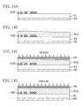
- a method for forming a flat insulating film a method including the steps of forming a flowable film by supplying a material with flowability onto a substrate, pressing the flowable film with a flat pressing face of a pressing member for planarizing the surface of the flowable film and solidifying the flowable film whose surface has been planarized is known as disclosed in, for example, Patent document 1.
- Patent document 1 Japanese Laid-Open Patent Publication No. 2000-350934
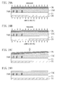
- FIGS. 21A through 21C and 22A through 22C will be described with reference to FIGS. 21A through 21C and 22A through 22C.
- a material with flowability such as a material in the form of a liquid or a gel
- a step substrate composed of a substrate 101 of a semiconductor wafer and a layer having irregularities (hereinafter simply referred to as the step layer) 102 formed on the substrate 101, so as to form a film with flowability (hereinafter simply referred to as the flowable film) 103A on the step substrate.
- a flat pressing face of a pressing member 104 is opposed to the surface of the flowable film 103A, and thereafter, as shown in FIG. 21C, the flowable film 103A is pressed toward the step substrate by applying a pressure toward the substrate to the pressing member 104, so as to planarize the surface of the flowable film 103A.
- the surface of the flowable film 103A is planarized over the whole surface of the substrate 101 simply by pressing the flowable film 103A with the pressing face of the pressing member 104.
- the flowable film 103A is annealed for causing a chemical reaction within the flowable film 103A, so as to solidify the flowable film 103A.
- a film having been solidified hereinafter simply referred to as the solidified film
- the solidified film having a flat top face is formed.
- the temperature of the solidified film 103B is lowered to room temperature, and thereafter, as shown in FIG. 22B, the pressing member 104 is moved away from the solidified film 103B.
- the solidified film 103B having a flat top face can be formed on the step substrate.
- multilayered interconnects are formed by repeating the damascene method in which a buried interconnect is formed by depositing a metal film on an insulating film for filling a concave portion formed in the insulating film and removing an unnecessary portion of the metal film by the CMP
- global level differences are accumulated in the CMP. Therefore, there arises a problem that the heights of the multilayered interconnects from a substrate are largely varied.
- the structure of the basic skeleton of the insulating film becomes locally ununiform when they are annealed at a temperature of 350°C or more in the solidifying process, which leads to degradation of the film quality that the dielectric coefficient of the insulating film is varied in accordance with the position within the insulation film.
- the insulating film cannot attain sufficient reliability, and hence, the performance and the reliability of the semiconductor device are largely degraded.
- an object of the invention is forming, through a small number of processes, an insulating film that has a high film quality with a uniform structure of a basic skeleton and has a minimum global level difference.
- the first method for forming a semiconductor device of this invention includes the steps of forming, on a substrate, a flowable film made of an insulating material with flowability; planarizing a top face of the flowable film by pressing the flowable film with a flat pressing face of a pressing member; forming a solidified film with a flat top face by solidifying the flowable film whose top face has been planarized through annealing of the flowable film performed at a first temperature with the pressing face pressed against the flowable film; and forming a burnt film with a flat top face by burning the solidified film through annealing of the solidified film with a flat top face performed at a second temperature higher than the first temperature.
- the solidifying process and the burning process are performed. Therefore, an insulating film made of the burnt film with a minimum global level difference and a flat top face can be formed through a small number of processes. Also, the annealing is performed on the flowable film at the first temperature that is a relatively low temperature, and thus, the basic skeleton of the solidified film (such as a polymer skeleton of an organic film, a siloxane skeleton of a silicon oxide film or an organic-inorganic film, or a resin skeleton of a resist film) is formed.
- the basic skeleton of the solidified film such as a polymer skeleton of an organic film, a siloxane skeleton of a silicon oxide film or an organic-inorganic film, or a resin skeleton of a resist film
- the annealing is performed on the solidified film at the second temperature that is a relatively high temperature, so as to vaporize porogen such as an acrylic polymer, a remaining solvent or the like from the solidified film. Therefore, as compared with the case where formation of a basic skeleton and vaporization of the porogen, a remaining solvent or the like are performed in parallel, the structure of the basic skeleton of the insulating film made of the burnt film is uniform, resulting in improving the film quality of the insulating film. Accordingly, the dielectric constant of the insulating film is uniform within the whole film, and the insulating film attains high reliability.
- the second method for forming a semiconductor device of this invention includes the steps of forming, on a substrate, a flowable film made of an insulating material with flowability over the substrate including a buried interconnect formed and exposed on the substrate; planarizing a top face of the flowable film by pressing the flowable film with a flat pressing face of a pressing member; forming a solidified film with a flat top face by solidifying the flowable film whose top face has been planarized through annealing of the flowable film performed at a first temperature with the pressing face pressed against the flowable film; forming a burnt film with a flat top face by burning the solidified film through annealing of the solidified film with a flat top face performed at a second temperature higher than the first temperature; and forming a buried plug connected at least to the interconnect by forming a via hole in the burnt film and filling the via hole with a metal material.
- the solidifying process and the burning process are performed. Therefore, an insulating film made of the burnt film with a minimum global level difference and a flat top face can be formed through a small number of processes. Also, the annealing is performed on the flowable film at the first temperature that is a relatively low temperature, and thus, the basic skeleton of the solidified film is formed. Thereafter, the annealing is performed on the solidified film at the second temperature that is a relatively high temperature, so as to vaporize porogen such as an acrylic polymer, a remaining solvent or the like from the solidified film.
- the structure of the basic skeleton of the insulating film made of the burnt film is uniform, resulting in improving the film quality of the insulating film. Accordingly, the dielectric constant of the insulating film is uniform within the whole film, and the insulating film attains high reliability.
- the third method for forming a semiconductor device of this invention includes the steps of forming, on a substrate, a flowable film made of an insulating material with flowability over the substrate including a buried plug formed and exposed on the substrate; planarizing a top face of the flowable film by pressing the flowable film with a flat pressing face of a pressing member; forming a solidified film with a flat top face by solidifying the flowable film whose top face has been planarized through annealing of the flowable film performed at a first temperature with the pressing face pressed against the flowable film; forming a burnt film with a flat top face by burning the solidified film through annealing of the solidified film with a flat top face performed at a second temperature higher than the first temperature; and forming a buried interconnect connected at least to the plug by forming an interconnect groove in the burnt film and filling the interconnect groove with a metal material.
- the solidifying process and the burning process are performed. Therefore, an insulating film made of the burnt film with a minimum global level difference and a flat top face can be formed through a small number of processes. Also, the annealing is performed on the flowable film at the first temperature that is a relatively low temperature, and thus, the basic skeleton of the solidified film is formed. Thereafter, the annealing is performed on the solidified film at the second temperature that is a relatively high temperature, so as to vaporize porogen such as an acrylic polymer, a remaining solvent or the like from the solidified film.
- the structure of the basic skeleton of the insulating film made of the burnt film is uniform, resulting in improving the film quality of the insulating film. Accordingly, the dielectric constant of the insulating film is uniform within the whole film, and the insulating film attains high reliability.
- the first temperature is preferably approximately 150°C through approximately 300°C.
- the basic skeleton of the flowable film can be formed without vaporizing the porogen or the like included in the flowable film.
- the second temperature is preferably approximately 350°C through approximately 450°C.
- the porogen or the like can be vaporized from the solidified film without degrading the film quality of the solidified film and also the film quality of the burnt film.
- the insulating material with flowability is preferably in the form of a liquid or a gel.
- the flowable film can be easily and definitely formed.
- the flowable film is preferably formed on the substrate by supplying the insulating material with flowability onto the substrate rotated.
- the thickness of the flowable film can be made uniform.
- the flowable film is preferably formed on the substrate by supplying the insulating material with flowability onto the substrate and rotating the substrate after the supply.
- the thickness of the flowable film can be made uniform.
- the flowable film in the step of forming a flowable film, is preferably formed on the substrate by supplying, in the form of a shower or a spray, the insulating material with flowability onto the substrate rotated.
- the flowable film can be definitely formed in a comparatively small thickness.
- the flowable film is preferably formed on the substrate by supplying the insulating material with flowability from a fine spray vent of a nozzle onto the substrate with the nozzle having the fine spray vent and the substrate relatively moved along plane directions.
- the thickness of the flowable film can be controlled to be a desired thickness by adjusting the relative moving rates of the nozzle and the substrate. Also, the degree of the flowability of the flowable film can be changed by adjusting the viscosity of the material with flowability. Furthermore, the process speed can be controlled by adjusting the number of nozzles.
- the flowable film is preferably formed on the substrate by supplying the insulating material with flowability having been adhered to a surface of a roller onto the substrate with the roller rotated.
- the thickness of the flowable film can be controlled by adjusting a distance between the roller and the substrate and a force for pressing the roller against the substrate. Also, a material with flowability and high viscosity can be used.
- Each of the first through third methods for forming a semiconductor device preferably further includes, between the step of forming a flowable film and the step of planarizing a top face of the flowable film, a step of selectively removing a peripheral portion of the flowable film.
- the peripheral portion of the substrate can be mechanically held in the process for forming the burnt film with ease.
- any of the first through third methods for forming a semiconductor device includes the step of selectively removing a peripheral portion of the flowable film
- this step is preferably performed by supplying a solution for dissolving the insulating material with flowability onto the peripheral portion of the flowable film with the flowable film rotated.
- the flowable film can be definitely removed from a peripheral portion of a substrate in the plane shape of a circle or a polygon with a large number of vertexes.
- any of the first through third methods for forming a semiconductor device includes the step of selectively removing a peripheral portion of the flowable film, this step is preferably performed by modifying the peripheral portion of the flowable film through irradiation with light and removing the modified peripheral portion.
- the flowable film can be definitely removed from a peripheral portion of a substrate not only in the plane shape of a circle or a polygon with a large number of vertexes but also in the shape of a polygon with a small number of vertexes such as a triangle or a rectangle.
- any of the first through third methods for forming a semiconductor device in the step of planarizing a top face of the flowable film, it is preferred that a plurality of distances between a surface of the substrate and the pressing face are measured, and that the flowable film is pressed with the pressing face in such a manner that the plurality of distances are equal to one another.
- a distance of the surface of the flowable film from the surface of the substrate can be always made uniform, and therefore, an operation for making uniform a distance between the surface of the substrate and the pressing face of the pressing member every given period of time can be omitted.
- each of the first through third methods for forming a semiconductor device in the step of planarizing a top face of the flowable film, it is preferred that a plurality of distances between a surface of a stage where the substrate is placed and the pressing face are measured, and that the flowable film is pressed with the pressing face in such a manner that the plurality of distances are equal to one another.
- a distance of the surface of the flowable film from the surface of the substrate can be always made uniform, and therefore, an operation for making uniform a distance between the surface of the substrate and the pressing face of the pressing member every given period of time can be omitted.
- the plurality of distances between the surface of the substrate or the stage and the pressing face are measured, the plurality of distances are preferably measured by measuring capacitance per unit area in respective measurement positions.
- the plural distances can be easily and definitely measured.
- the pressing face of the pressing member preferably has a hydrophobic property.
- the pressing member can be easily moved away from the solidified film, and therefore, a solidified film with fewer defects and also a burnt film with fewer defects can be formed.
- the insulating material with flowability is a photo-setting resin
- the step of forming a solidified film includes a sub-step of irradiating the flowable film with light.
- the flowable film can be easily and rapidly solidified through a photochemical reaction and a thermal chemical reaction.
- the insulating material with flowability is preferably an organic material, an inorganic material, an organic-inorganic material, a photo-setting resin or a photosensitive resin.
- the solidified film in the step of forming a burnt film, is preferably annealed at the second temperature with the pressing face pressed against the solidified film.
- the solidified film in the step of forming a burnt film, is preferably annealed at the second temperature with the pressing face moved away from the solidified film.
- the porogen, the remaining solvent or the like included in the solidified film can be easily vaporized.
- the burnt film is preferably a porous film.
- an insulating film made of the burnt film with a low dielectric constant can be formed.
- the burnt film preferably has a dielectric constant of approximately 4 or less.
- the dielectric constant of the insulating film can be definitely lowered, so as to reduce capacitance between metal interconnects.
- the second method for forming a semiconductor device preferably further includes, before the step of forming a flowable film, a step of forming the buried interconnect exposed on the substrate by forming a buried interconnect in an organic film formed on the substrate and removing the organic film.
- the third method for forming a semiconductor device preferably further includes, before the step of forming a flowable film, a step of forming the buried plug exposed on the substrate by forming a buried plug in an organic film formed on the substrate and removing the organic film.
- the organic film is preferably removed by wet etching in the step of forming the buried interconnect or the buried plug.
- the organic film is preferably removed by dry etching in the step of forming the buried interconnect or the buried plug.
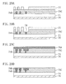
- Embodiment 1 A method for forming a semiconductor device according to Embodiment 1 will now be described with reference to FIGS. 1A through 1D and 2A through 2C.
- a material with flowability such as a material in the form of a liquid or a gel, is supplied onto the step layer 11, so as to form a flowable film 12A.
- the plane shape of the substrate 10 is not particularly specified and may be any shape including a circle, a polygon and the like.
- annealing is performed at approximately 80°C through 120°C in order to vaporize a part or most of a solvent included in the flowable film 12A formed above the substrate 10.
- This annealing is generally designated as pre-bake, and the temperature of the pre-bake may be set so that the flowability of the flowable film 12A can be kept in a planarizing process subsequently performed.
- the temperature may be set in accordance with the characteristics (such as the boiling point) of the solvent used for supplying the material with flowability, and the pre-bake may be omitted in some cases.
- the flowable film 12A may be, for example, an organic film, an inorganic film, an organic-inorganic film (organic-inorganic hybrid film), a photo-setting resin film that is cured through irradiation with light, a photosensitive resin film such as a resist film, a porous film having a large number of pores with a diameter of approximately 1 nm through 10 nm therein, or the like.
- a method for forming the flowable film 12A may be a spin coating method, a microscopic spraying method, a rotation roller method or the like, the thickness of the flowable film 12A is adjusted differently depending upon the employed method, and the film thickness can be adjusted by selecting the method for forming the flowable film 12A.
- the method for forming the flowable film 12A will be described in detail in Examples 1 through 4 below.
- the material with flowability is preferably an insulating material.
- a flat pressing face of a pressing member 13 is opposed to the surface of the flowable film 12A, and thereafter, as shown in FIG. 1C , a pressure toward the substrate is applied to the pressing member 13, so as to planarize the whole top face of the flowable film 12A.
- the flowable film 12A is annealed at a first temperature (T1) so as to cause a chemical reaction within the flowable film 12A.
- T1 a first temperature
- the first temperature (T1) is preferably approximately 150°C through approximately 300°C and is more preferably approximately 200°C through approximately 250°C.
- the basic skeleton of the flowable film 12A such as a polymer skeleton or a siloxane skeleton, is definitely formed.
- the annealing is performed with a hot plate set to a desired temperature for approximately 2 through 3 minutes.
- the solidified film 12B is annealed at a second temperature ( T2 ) higher than the first temperature (T1) for burning the solidified film 12B.
- T2 a burnt film 12C made of the solidified film 12B burnt and having a flat top face is formed.
- the second temperature ( T2 ) is preferably approximately 350°C through approximately 450°C.
- porogen or the like is vaporized from the solidified film 12B where the basic skeleton has been formed, and hence, the burnt film 12C with a uniform film quality can be obtained.
- the annealing is performed with a hot plate set to a desired temperature for approximately 2 through approximately 15 minutes.
- the pressing member 13 is moved away from the burnt film 12C, and thereafter, the temperature of the burnt film 12C is ultimately lowered to room temperature.
- the burnt film 12C that is flat in the whole top face is obtained.
- the pressing face of the pressing member 13 is preferably subjected to a Teflon (registered trademark) coating treatment or a surface treatment with a silicon coupling material.
- a Teflon (registered trademark) coating treatment or a surface treatment with a silicon coupling material are preferably subjected to a Teflon (registered trademark) coating treatment or a surface treatment with a silicon coupling material.
- the material with flowability used for forming an organic film is, for example, an aromatic polymer having aryl ether as a principal skeleton, and specific examples are FLARE and GX-3 (manufactured by Honeywell) and SiLK (manufactured by Dow Chemical).
- the material with flowability used for forming an inorganic film is, for example, HSQ (hydrogen silsquioxane) or organic SOG such as an alkylsiloxane polymer, and a specific example of the HSQ is Fox (manufactured by Dow Coming) and a specific example of the organic SOG is HSG-RZ25 (manufactured by Hitachi Chemical Co., Ltd.).
- HSQ hydrogen silsquioxane
- organic SOG such as an alkylsiloxane polymer
- HSG-RZ25 manufactured by Hitachi Chemical Co., Ltd.
- the material with flowability used for forming an organic-inorganic film is, for example, organic siloxane having an organic group such as a methyl group in a siloxane skeleton, and a specific example is HOSP (hybrid organic siloxane polymer) (manufactured by Honeywell).
- HOSP hybrid organic siloxane polymer
- the material with flowability used for forming a photo-setting resin film is, for example, PDGI (polydimethyl glutar imide), and a specific example is SAL101 (manufactured by Shipley Far East).
- the material with flowability used for forming a photosensitive resin film may be a general resist material used in the lithography.
- the material with flowability used for forming a porous film is, for example, an organic, inorganic or organic-inorganic material having pores
- a specific example of the organic material having pores is Porous FLARE (manufactured by Honeywell)
- a specific example of the inorganic material having pores is XLK (manufactured by Dow Corning) having pores in HSQ (hydrogen silsquioxane)
- specific examples of the organic-inorganic material having pores are Nanoglass (manufactured by Honeywell) and LKD-5109 (manufactured by JSR).
- the burnt film 12C obtained by solidifying and burning the flowable film 12A made of any of the aforementioned materials is used as an interlayer insulating film of multilayered interconnects
- an interlayer insulating film that is dense and has a lower dielectric constant than a general silicon oxide film (with a dielectric constant of approximately 4) can be obtained. Therefore, a film suitable to a semiconductor device refined to 100 nm or less can be realized.
- an interlayer insulating film with a very low dielectric constant of 2 or less can be realized.
- Embodiment 2 A method for forming a semiconductor device according to Embodiment 2 will now be described with reference to FIGS. 1A through 1D and 2A through 2C.
- Embodiment 2 Since the basic process sequence of Embodiment 2 is almost the same as that of Embodiment 1, a difference from that of Embodiment 1 will be principally described below.
- a flowable film 12A is formed on the step layer 11. Thereafter, a pressing member 13 is pressed against the flowable film 12A, so as to planarize the whole top face of the flowable film 12A.
- the flowable film 12A is annealed at a first temperature ( T1 ), so as to form a solidified film 12B having a flat top face.
- the solidified film 12B is annealed at a second temperature ( T2 ) higher than the first temperature (T1) for burning the solidified film 12B, thereby forming a burnt film 12C made of the burnt solidified film 12B. Thereafter, the temperature of the burnt film 12C is lowered to approximately room temperature. Thus, the burnt film 12C having a flat top face is formed.
- Embodiment 1 A difference between Embodiment 1 and Embodiment 2 is that the solidified film 12B is burnt with the pressing face of the pressing member 13 pressed against the solidified film 12B in Embodiment 1 while it is burnt with the pressing face of the pressing member 13 moved away from the solidified film 12B in Embodiment 2. Accordingly, in Embodiment 2, it is necessary to perform the annealing with a hot plate in the solidifying process but the annealing can be performed with a hot plate or a furnace in the burning process.
- Embodiment 2 is more effective than Embodiment 1 in the case where a solidified film largely outgassing is annealed in the burning process.
- concentration of a remaining solvent in the film can be controlled through the pre-bake, and therefore, the film minimally outgases in the burning process, but depending upon the composition of the film, it may outgas in the burning process where the annealing is performed at a comparatively high temperature.
- a porous film In a porous film, most of the basic structure of the film is formed through the annealing performed at the first temperature (T1) in the solidifying process, and a pore forming material added for forming pores is vaporized through the annealing performed at the second temperature (T2) in the burning process. Therefore, the burning process of Embodiment 2 in which the film is burnt with the pressing member 13 moved away from the solidified film 12B is suitable. Even in a porous film, if it is an optimal film in which the basic skeleton of the film is formed and most of a pore forming material is vaporized in the solidifying process, a good burnt film 12C can be obtained even by employing the burning process of Embodiment 1.
- the annealing temperature of the burning process (the second temperature) is set to be higher than the annealing temperature of the solidifying process (the first temperature).
- the annealing temperature of the solidifying process (the first temperature) is preferably approximately 150°C through 300°C
- the annealing temperature of the burning process (the second temperature) is preferably approximately 350°C through 450°C.
- a film having a flat top face is formed through one annealing in a film curing process performed after pressing with a pressing member (a mold).
- a flat burnt film 12C is formed through the annealing performed in the two stages in the solidifying process and the burning process.
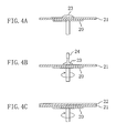
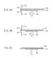
- FIG. 4A after holding a substrate 21 through vacuum adsorption on a rotatable stage 20, an appropriate amount of material 23 with flowability is dropped on the substrate 21, and thereafter, the stage 20 is rotated.
- FIG. 4B after holding a substrate 21 through vacuum adsorption on a rotatable stage 20, a material 23 with flowability is supplied from a dropping nozzle 24 onto the substrate 21 while rotating the stage 20 together with the substrate 21.
- a flowable film 22 is formed on the substrate 21 as shown in FIG. 4C .
- the flowable film 22 can attain hardness suitable for the process for transferring the flat surface of the pressing face of the pressing member 13 (see FIG. 1B or 2B) onto the flowable film 22.
- Example 1 It is noted that the method of Example 1 is suitable to a case where the flowable film 22 is formed in a comparatively large thickness.
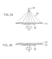
- a material 26 with flowability is supplied in the form of a shower or spray from a spray nozzle 25 onto the substrate 21 while rotating the stage 20 together with the substrate 21.
- the stage 20 After supplying a desired amount of material 26 with flowability, the stage 20 is continuously rotated for a predetermined period of time. Thus, a flowable film 22 is formed on the substrate 21 as shown in FIG. 5B.
- Example 2 The method of Example 2 is suitable to a case where the flowable film 22 is formed in a comparatively small thickness.
- a material 28 with flowability is supplied from a dropping nozzle 27 onto a substrate 21 by a given amount at a time while moving the substrate 21 along one of the two perpendicular directions of the two-dimensional rectangular coordinate system, for example, along the lateral direction of FIG. 6A and moving the dropping nozzle 27 along the other of the two perpendicular directions, for example, along the longitudinal direction of FIG. 6A.
- an operation for moving the substrate 21 by a given distance toward the leftward direction in FIG. 6A and stopping it is repeatedly performed, and while the substrate 21 is stopped, the material 28 with flowability is supplied from the dropping nozzle 27 onto the substrate 21 by a given amount at a time while moving the dropping nozzle 27 along the longitudinal direction in FIG. 6A.
- a flowable film 22 is formed on the substrate 21 as shown in FIG. 6B.
- the thickness of the flowable film 22 can be controlled over a range from a small thickness to a large thickness by adjusting the amount of material 28 with flowability supplied from the dropping nozzle 27 and the moving rate of the dropping nozzle 27.
- the degree of the flowability of the flowable film 22 can be changed by adjusting the viscosity of the material 28 with flowability supplied from the dropping nozzle 27.
- the process speed can be controlled by adjusting the number of dropping nozzles 27.
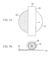
- the thickness of the flowable film 22 can be controlled by adjusting the distance between the rotation roller 29 and the substrate 21 and a force for pressing the rotation roller 29 against the substrate 21.
- Example 4 is suitable to a case where the material 30 with flowability is in the form of a highly viscous liquid or a gel.
- Embodiment 3 methods for selectively removing a peripheral portion of the flowable film obtained in Embodiment 1 or 2 are described. Specifically, in a first method, the peripheral portion is removed by supplying a solution for dissolving the flowable film to the peripheral portion of the flowable film while rotating the substrate on which the flowable film is formed, and in a second method, the peripheral portion of the flowable film is modified by irradiating the peripheral portion with light and thereafter the modified peripheral portion is removed.
- the flowable film is formed over the whole surface of the substrate, namely, also on a peripheral portion of the substrate. However, it is sometimes necessary to mechanically hold the peripheral portion of the substrate.
- Embodiment 3 is devised for overcoming such a problem, and since the peripheral portion of the flowable film is selectively removed in Embodiment 3, the peripheral portion of the substrate can be easily mechanically held.
- a release solution 33 is supplied from a first nozzle 31 to the peripheral portion of the flowable film 22 and a release solution 34 is supplied from a second nozzle 32 to the back surface of the peripheral portion of the substrate 21.
- the peripheral portion of the flowable film 22 can be removed as well as the material with flowability having been adhered onto the peripheral portion of the back surface of the substrate 21 can be removed.
- the first method is preferably performed before the transferring process for the flowable film 22.
- this method is suitable when the plane shape of the substrate 21 is in the shape of a circle or a polygon with a large number of vertexes.
- the stage 20 is rotated for rotating the flowable film 22, and the peripheral portion of the flowable film 22 is irradiated with light 36 emitted from a photoirradiation device 35, so as to modify the peripheral portion by causing a photochemical reaction in the peripheral portion (irradiated portion) of the flowable film 22.
- the light 36 used in this case is preferably UV or light of a shorter wavelength than UV.
- a solution 37 such as a developer is supplied over the flowable film 22.
- the peripheral portion of the flowable film 22 having been modified is dissolved in the solution 37, and hence, the peripheral portion of the flowable film 22 can be selectively removed.
- the stage 20 is rotated together with the flowable film 22 again, so as to remove the solution 37 remaining on the flowable film 22 to the outside by using centrifugal force.
- a rinsing solution is preferably supplied onto the flowable film 22 so as to remove the solution 37 still remaining. In this manner, the flowable film 22 whose peripheral portion has been selectively removed can be obtained.
- the second method is preferably performed before the transferring process for the flowable film 22.
- this method is applicable not only when the plane shape of the substrate 21 is in the shape of a circle or a polygon with a large number of vertexes but also when it is in the shape of a polygon with a small number of vertexes such as a triangle or a rectangle.
- FIGS. 10A, 10B, 11A and 11B A method for forming a semiconductor device according to Embodiment 4 will now be described with reference to FIGS. 10A, 10B, 11A and 11B.
- Embodiment 4 a preferable method for planarizing the top face of the flowable film obtained in Embodiment 1 or 2 is described, and in this method, a plurality of distances between the surface of the substrate or the stage and the pressing face of the pressing member are measured and the flowable film is pressed in such a manner that these plural distances are equal to one another.
- a pressing member 43 having a plurality of distance sensors 44 on its flat pressing face is used for planarizing the top face of the flowable film 42.
- the outside dimension of the stage 20 is preferably larger than that of the substrate 40.
- a plurality of distances between the surface of the substrate 40 or the surface of the stage 20 (see FIG. 4C or 5B) on which the substrate 40 is placed and the pressing face of the pressing member 43 are measured with the plural distance sensors 44, and the flowable film 42 is planarized by pressing the flowable film 42 with the pressing member 43 in such a manner that the plural distances are equal to one another.
- information of the plural distances measured with the plural distance sensors 44 is fed back to pressing means for pressing the pressing member 43, so that the flowable film 42 can be pressed in such a manner that the plural distances are equal to one another.
- the feedback control may be executed by using a computer.
- each distance is preferably measured by measuring capacitance per unit area in the corresponding measurement position.
- a, b, c, ... and q denote positions where the distance sensors 44 are respectively provided.
- the positions a through q are preferably optimized in accordance with the mechanism of the pressing member 43 so as to be set to positions where the distances between the surface of the substrate 40 or the surface of the stage where the substrate 40 is placed and the surface of the flowable film 42 can be efficiently measured.
- the sensor positions a through i at the center are suitable to measure the distances between the surface of the substrate 40 and the surface of the flowable film 42
- the sensor positions j through q in the peripheral portion are suitable to measure the distances between the surface of the stage where the substrate 40 is placed and the surface of the flowable film 42.
- the distances between the surface of the substrate 40 and the surface of the flowable film 42 may be measured with the distance sensors 44 provided in the sensor positions a through i alone, merely the distances between the surface of the stage where the substrate 40 is placed and the surface of the flowable film 42 may be measured with the distance sensors 44 provided in the sensor positions j through q alone, or the distances between the surface of the substrate 40 and the surface of the flowable film 42 and the distances between the surface of the stage where the substrate 40 is placed and the surface of the flowable film 42 may be measured with the distance sensors 44 provided in the sensor positions a through q.
- the distances between the surface of the substrate 40 and the surface of the flowable film 42 may be adjusted with the distance sensors 44 provided in the sensor positions j through q.
- the distance sensors 44 may be optimized in accordance with a desired degree of flatness.
- Embodiment 1 it is significant but is not easy to equalize a distance of the surface of the flowable film 12A from the surface of the substrate 10.
- the distance of the surface of the flowable film 12A from the surface of the substrate 10 can be made uniform by previously setting the distance between the surface of the substrate 10 and the pressing face of the pressing member 13 to be uniform.
- the distance of the surface of the flowable film 42 from the surface of the substrate 40 can be always uniform, and hence, an operation for making the distance between the surface of the substrate 40 and the pressing face of the pressing member 43 uniform every given period of time can be omitted.
- the process for adjusting the distance between the surface of the substrate 40 and the pressing face of the pressing member 43 to be uniform may be performed before, while or after pressing the flowable film 42 with the pressing member 43.
- FIG. 11A shows a cross-section of the flowable film 42 obtained when the distance between the pressing face of the pressing member 43 and the surface of the substrate 40 provided below a step layer 41 is ununiform
- FIG. 11B shows a cross-section of the flowable film 42 obtained when the distance between the pressing face of the pressing member 43 and the surface of the substrate 40 is kept uniform.
- the top face of the flowable film 42 can be planarized with the distance of the flowable film 42 from the surface of the substrate 40 kept uniform.
- FIGS. 12A and 12B A method for forming a semiconductor device according to Embodiment 5 will now be described with reference to FIGS. 12A and 12B.
- a flowable film 52A is solidified by annealing the flowable film 52A while irradiating it with light.
- the flowable film 52A is irradiated with light and annealed.
- the light used for the irradiation is, when the flowable film 52A is solidified principally through a photochemical reaction, preferably UV or light of a shorter wavelength than UV, and when the flowable film 52A is solidified principally through a thermal chemical reaction, preferably infrared light.
- the flowable film 52A is solidified through the photochemical reaction or the thermal chemical reaction, resulting in giving a solidified film 52B as shown in FIG. 12B.
- the method for solidifying the flowable film 52A principally through the photochemical reaction is suitable to a film of a photo-setting resin, such as a photosensitive resin film like a photoresist used in the lithography.
- the method for solidifying the flowable film 52A principally through the thermal chemical reaction is suitable to an organic film, an organic-inorganic film or an inorganic film made of a chemically amplified material composed of a material for generating an acid or a base through irradiation with light and a base polymer solidified by an acid or a base.
- FIGS. 13A through 13F, 14A through 14D, 15A through 15D and 16A through 16D A method for forming a semiconductor device according to Embodiment 6 will now be described with reference to FIGS. 13A through 13F, 14A through 14D, 15A through 15D and 16A through 16D.
- an organic film 62 of, for example, a photoresist film, an organic low-k film or the like is formed on the interlayer insulating film 61 by the spin coating method or the chemical vapor deposition (CVD) method as shown in FIG. 13B.
- the organic film 62 preferably includes a material having an antireflection function corresponding to the wavelength of exposing light used in subsequently performed lithography.
- a process for forming an antireflection film below the organic film 62 can be omitted.
- an inorganic film or an organic-inorganic film may be used.
- an SOG film or the like formed by the spin coating method may be used.
- an SOG film that is not completely crosslinked but partly unreacted through baking at a temperature of approximately 200°C through approximately 300°C is used.
- an SOD (spin-on-dielectric) film recently frequently used as a low-k film material may be used.
- the organic film 62 is dry etched by using the first resist pattern 63 as a mask, so as to form an interconnect groove 62a in the organic film 62 as shown in FIG. 13D.
- an etching gas including, as a principal component, a mixed gas of an oxygen gas and a nitrogen gas or a mixed gas of a nitrogen gas and a hydrogen gas can be used.
- a first metal film 64A of Cu, Ag, Au, Pt or the like is deposited on the barrier metal layer by, for example, the plating method.
- an unnecessary portion of the first metal film 64A namely, a portion thereof exposed above the organic film 62, is removed by the CMP, so as to form a buried interconnect 64B made of the first metal film 64A.
- etching is performed for removing the organic film 62 and exposing the buried interconnect 64B.
- a diffusion preventing film (not shown in the drawing) is formed on the buried interconnect 64B by, for example, the CVD.
- the dry etching of the organic film 62 may be anisotropic or isotropic.
- a single-layer film of a Si 3 N 4 film, a SiC film or a SiCN film, or a multilayered film of such a film and a SiCO film can be used as the diffusion preventing film.
- a flowable film 65A is formed on the buried interconnect 64B having the diffusion preventing film by supplying an insulating material with flowability in the form of a liquid or a gel by the spin coating method, the microscopic spraying method, the rotation roller method or the like in the same manner as in Embodiment 1.
- the thickness of the flowable film 65A can be appropriately set.
- the flowable film 65A may be any of the insulating films described in Embodiment 1, namely, an organic film, an inorganic film, an organic-inorganic film or a porous film.
- an insulating film When such an insulating film is used, the resultant insulating film attains a lower dielectric constant than a general silicon oxide film, and thus, a film suitable to a semiconductor device refined to 100 nm or less can be realized.
- a porous film is used as the flowable film 65A, an insulating film with a very low dielectric constant of 2 or less can be realized.
- FIG. 14C After a flat pressing face of a pressing member 66 is brought into contact with the surface of the flowable film 65A, a pressure is applied to the pressing member 66 so as to planarize the top face of the flowable film 65A as shown in FIG. 14D.
- the top face of the flowable film 65A is made to be placed at the uniform height from the surface of the substrate 61.
- the substrate 60 together with the flowable film 65A are annealed at a first temperature (T1) so as to cause a thermal chemical reaction in the insulating material.
- T1 a first temperature
- the flowable film 65A is solidified to form a solidified film 65B with a flat top face.
- any of the methods of Embodiments 1 through 4 suitable to the characteristics of the flowable film 65A may be selected.
- the solidified film 65B is annealed at a second temperature (T2) higher than the first temperature (T1) for burning the solidified film 65B, so as to form a burnt film 65C that is made of the solidified film 65B burnt and has a flat top face.
- T2 second temperature
- T1 first temperature
- the pressing member 66 is moved away from the burnt film 65C and the temperature of the burnt film 65C is lowered ultimately to room temperature.
- the burnt film 65C having a flat top face is obtained.
- the burnt film 65C is subjected to the CMP or the etch back process.
- the burnt film 65C is dry etched by using the second resist pattern 67 as a mask, so as to form a via hole 68 in the burnt film 65C as shown in FIG. 16B.
- an etching gas including fluorine such as a CF 4 gas or a CHF 3 gas, can be used.
- the diffusion preventing film (not shown in the drawing) formed on the buried interconnect 64B is dry etched, so as to expose the buried interconnect 64B.
- a second metal film 69A of, for example, copper is deposited over the barrier metal layer by, for example, the plating method.
- the second metal film 69A is preferably grown by using, as a seed, a seed layer previously formed on the barrier metal layer by the sputtering.
- the second metal film 69A may be deposited by the CVD or the like instead of the plating method and that silver, gold, platinum or the like may be used instead of copper. These metals are preferred because they can be easily deposited by the plating method and have low resistance.
- the burnt film 65C with no global level difference can be formed in Embodiment 6, local concentration of the film can be released in the insulating film, resulting in improving the reliability of the multilayered interconnects. Also, since the burnt film 65C having a flat top face can be obtained, in the case where a mask pattern is formed on the burnt film 65C by the lithography, degradation of a focal depth margin derived from a level difference can be suppressed. Therefore, as compared with conventional technique, a process margin (process window) can be increased, resulting in forming a highly accurate semiconductor device.
- the burning process of Embodiment 2 is more effectively employed than that of Embodiment 1.
- the concentration of a solvent remaining in the flowable film 65A can be controlled through the pre-bake, and hence, the film minimally outgases in the burning process.
- the film may largely outgas in some cases in the burning process where the film is annealed at a comparatively high temperature. In such a case, when the burning process of Embodiment 1 is employed, there arises a problem of uniformity or stability in the burnt film, and hence, the burning process of Embodiment 2 is preferably employed.
- the burnt film 65C is a porous film
- the effect of the burning process of Embodiment 2 is exhibited.
- a porous film most of the basic structure of the solidified film 65B is formed in the annealing performed at the first temperature (T1) of the solidifying process, and a pore forming material added for forming pores is vaporized in the annealing performed at the second temperature ( T2 ) of the following burning process. Therefore, the burning process of Embodiment 2 where the film is burnt with the pressing member 66 moved away from the solidified film 65B is suitable.
- the annealing temperature of the solidifying process (the first temperature) is preferably approximately 150°C through 300°C, and the annealing temperature of the burning process (the second temperature) is preferably approximately 350°C through 450°C.
- FIGS. 17A through 17F, 18A through 18D, 19A through 19D and 20A through 20D A method for forming a semiconductor device according to Embodiment 7 will now be described with reference to FIGS. 17A through 17F, 18A through 18D, 19A through 19D and 20A through 20D.
- an organic film 72 of, for example, a photoresist film, an organic low-k film or the like is formed on the interlayer insulating film 71 by the spin coating method or the chemical vapor deposition (CVD) method as shown in FIG. 17B.
- an inorganic film or an organic-inorganic film may be used.
- an SOG film or the like formed by the spin coating method may be used.
- an SOG film that is not completely crosslinked but partly unreacted through baking at a temperature of approximately 200°C through approximately 300°C is used.
- an SOD (spin-on-dielectric) film recently frequently used as a low-k film material may be used.
- the organic film 72 is dry etched by using the first resist pattern 73 as a mask, so as to form a via hole 72a in the organic film 72 as shown in FIG. 17D.
- a first metal film 74A of Cu, Ag, Au, Pt or the like is deposited on the barrier metal layer by, for example, the plating method.
- an unnecessary portion of the first metal film 74A namely, a portion thereof exposed above the organic film 72, is removed by the CMP, so as to form a buried plug 74B made of the first metal film 74A.
- etching is performed for removing the organic film 72 and exposing the buried plug 74B.
- a diffusion preventing film (not shown in the drawing) is formed on the buried plug 74B by, for example, the CVD.
- a flowable film 75A is formed on the buried plug 74B having the diffusion preventing film by supplying an insulating material with flowability in the form of a liquid or a gel by the spin coating method, the microscopic spraying method, the rotation roller method or the like in the same manner as in Embodiment 1.
- the flowable film 75A may be any of the insulating films described in Embodiment 1, namely, an organic film, an inorganic film, an organic-inorganic film or a porous film.
- the substrate 70 together with the flowable film 75A are annealed at a first temperature (T1) so as to cause a thermal chemical reaction in the insulating material.
- T1 a first temperature
- the flowable film 75A is solidified to form a solidified film 75B with a flat top face.
- any of the methods of Embodiments 1 through 4 suitable to the characteristics of the flowable film 75A may be selected.
- the solidified film 75B is annealed at a second temperature ( T2 ) higher than the first temperature (T1) for burning the solidified film 75B, so as to form a burnt film 75C that is made of the solidified film 75B burnt and has a flat top face.
- T2 second temperature
- T1 first temperature
- the pressing member 76 is moved away from the burnt film 75C and the temperature of the burnt film 75C is lowered ultimately to room temperature.
- the burnt film 75C having a flat top face is obtained.
- the burnt film 75C is dry etched by using the second resist pattern 77 as a mask, so as to form an interconnect groove 78 in the burnt film 75C as shown in FIG. 20B.
- the diffusion preventing film (not shown in the drawing) formed on the buried plug 74B is dry etched, so as to expose the buried plug 74B .
- a second metal film 79A of, for example, copper is deposited over the barrier metal layer by, for example, the plating method.
- the burnt film 75C with no global level difference can be formed in Embodiment 7, local concentration of stress can be released in the insulating film, resulting in improving the reliability of the multilayered interconnects. Also, since the burnt film 75C having a flat top face can be obtained, in the case where a mask pattern is formed on the burnt film 75C by the lithography, degradation of a focal depth margin derived from a level difference can be suppressed. Therefore, as compared with conventional technique, a process margin (process window) can be increased, resulting in forming a highly accurate semiconductor device.
- the annealing temperature of the solidifying process (the first temperature) is preferably approximately 150°C through 300°C, and the annealing temperature of the burning process (the second temperature) is preferably approximately 350°C through 450°C.
- the present invention is useful as a method for forming a semiconductor device.
Landscapes
- Internal Circuitry In Semiconductor Integrated Circuit Devices (AREA)
- Hall/Mr Elements (AREA)
- Formation Of Insulating Films (AREA)
Applications Claiming Priority (3)
| Application Number | Priority Date | Filing Date | Title |
|---|---|---|---|
| JP2003175882 | 2003-06-20 | ||
| JP2003175882 | 2003-06-20 | ||
| PCT/JP2004/008654 WO2004114388A1 (ja) | 2003-06-20 | 2004-06-14 | 半導体装置の製造方法 |
Publications (1)
| Publication Number | Publication Date |
|---|---|
| EP1553620A1 true EP1553620A1 (de) | 2005-07-13 |
Family
ID=33534878
Family Applications (1)
| Application Number | Title | Priority Date | Filing Date |
|---|---|---|---|
| EP04746147A Withdrawn EP1553620A1 (de) | 2003-06-20 | 2004-06-14 | Halbleiterbauelementeherstellungsverfahren |
Country Status (6)
| Country | Link |
|---|---|
| EP (1) | EP1553620A1 (de) |
| JP (1) | JPWO2004114388A1 (de) |
| KR (1) | KR20060017575A (de) |
| CN (1) | CN1698187A (de) |
| TW (1) | TW200504928A (de) |
| WO (1) | WO2004114388A1 (de) |
Cited By (2)
| Publication number | Priority date | Publication date | Assignee | Title |
|---|---|---|---|---|
| KR20200068579A (ko) * | 2018-12-05 | 2020-06-15 | 캐논 가부시끼가이샤 | 슈퍼스트레이트 및 그 사용 방법 |
| EP3637456A3 (de) * | 2018-10-11 | 2020-12-16 | Canon Kabushiki Kaisha | Filmausbildungsvorrichtung, filmausbildungsverfahren und verfahren zur herstellung eines artikels |
Families Citing this family (7)
| Publication number | Priority date | Publication date | Assignee | Title |
|---|---|---|---|---|
| WO2007058604A1 (en) * | 2005-11-18 | 2007-05-24 | Replisaurus Technologies Ab | Master electrode and method of forming the master electrode |
| JP2008300414A (ja) * | 2007-05-29 | 2008-12-11 | Dainippon Screen Mfg Co Ltd | 薄膜形成装置および薄膜形成方法 |
| JP7089375B2 (ja) * | 2018-02-19 | 2022-06-22 | キヤノン株式会社 | 平坦化装置 |
| JP7119617B2 (ja) * | 2018-06-15 | 2022-08-17 | 東京エレクトロン株式会社 | 塗布膜形成方法及び塗布膜形成装置 |
| JP7191606B2 (ja) * | 2018-09-14 | 2022-12-19 | キヤノン株式会社 | 型を用いて基板上の組成物を成形する成形装置、成形方法、及び、物品製造方法 |
| CN109546011B (zh) * | 2018-11-14 | 2021-04-23 | 京东方科技集团股份有限公司 | 膜层的制作方法、显示基板及其制作方法与设备 |
| JP7267783B2 (ja) * | 2019-03-07 | 2023-05-02 | キヤノン株式会社 | 平坦化装置、平坦化方法及び物品の製造方法 |
Family Cites Families (3)
| Publication number | Priority date | Publication date | Assignee | Title |
|---|---|---|---|---|
| US5679610A (en) * | 1994-12-15 | 1997-10-21 | Kabushiki Kaisha Toshiba | Method of planarizing a semiconductor workpiece surface |
| JP2002124513A (ja) * | 2000-10-13 | 2002-04-26 | Fujitsu Ltd | 基板の平坦化方法、半導体装置及びその製造方法 |
| JP3927768B2 (ja) * | 2000-11-17 | 2007-06-13 | 松下電器産業株式会社 | 半導体装置の製造方法 |
-
2004
- 2004-03-23 TW TW093107817A patent/TW200504928A/zh unknown
- 2004-06-14 JP JP2005507247A patent/JPWO2004114388A1/ja not_active Withdrawn
- 2004-06-14 CN CNA2004800005828A patent/CN1698187A/zh active Pending
- 2004-06-14 KR KR1020057001612A patent/KR20060017575A/ko not_active Withdrawn
- 2004-06-14 EP EP04746147A patent/EP1553620A1/de not_active Withdrawn
- 2004-06-14 WO PCT/JP2004/008654 patent/WO2004114388A1/ja not_active Ceased
Non-Patent Citations (1)
| Title |
|---|
| See references of WO2004114388A1 * |
Cited By (3)
| Publication number | Priority date | Publication date | Assignee | Title |
|---|---|---|---|---|
| EP3637456A3 (de) * | 2018-10-11 | 2020-12-16 | Canon Kabushiki Kaisha | Filmausbildungsvorrichtung, filmausbildungsverfahren und verfahren zur herstellung eines artikels |
| US11275309B2 (en) | 2018-10-11 | 2022-03-15 | Canon Kabushiki Kaisha | Film forming apparatus, film forming method, and method of manufacturing article |
| KR20200068579A (ko) * | 2018-12-05 | 2020-06-15 | 캐논 가부시끼가이샤 | 슈퍼스트레이트 및 그 사용 방법 |
Also Published As
| Publication number | Publication date |
|---|---|
| KR20060017575A (ko) | 2006-02-24 |
| TW200504928A (en) | 2005-02-01 |
| CN1698187A (zh) | 2005-11-16 |
| JPWO2004114388A1 (ja) | 2006-08-03 |
| WO2004114388A1 (ja) | 2004-12-29 |
Similar Documents
| Publication | Publication Date | Title |
|---|---|---|
| US7563709B2 (en) | Pattern formation method and method for forming semiconductor device | |
| KR102394042B1 (ko) | 사전패터닝된 리소그래피 템플레이트, 상기 템플레이트를 이용한 방사선 패터닝에 기초한 방법 및 상기 템플레이트를 형성하기 위한 방법 | |
| KR101283837B1 (ko) | 유전체 막의 처리 방법 및 피처 형성 방법 | |
| US20070202666A1 (en) | Method for fabricating semiconductor device | |
| US7291554B2 (en) | Method for forming semiconductor device | |
| JP2001077196A (ja) | 半導体装置の製造方法 | |
| US6972258B2 (en) | Method for selectively controlling damascene CD bias | |
| JP2007514291A (ja) | ビア・ファースト・デュアルダマシン相互接続配線形成のための構造体充填方法 | |
| US7598172B2 (en) | Method for manufacturing semiconductor device by using dual damascene process and method for manufacturing article having communicating hole | |
| US7723237B2 (en) | Method for selective removal of damaged multi-stack bilayer films | |
| EP1553620A1 (de) | Halbleiterbauelementeherstellungsverfahren | |
| US7192880B2 (en) | Method for line etch roughness (LER) reduction for low-k interconnect damascene trench etching | |
| US20050191860A1 (en) | Method for forming semiconductor device | |
| JP2005534168A (ja) | 層配置物および層配置物の製造方法 | |
| US20070232047A1 (en) | Damage recovery method for low K layer in a damascene interconnection | |
| JP3497725B2 (ja) | 半導体装置およびその製造方法 | |
| US20020177300A1 (en) | Method for forming an opening in polymer-based dielectric |
Legal Events
| Date | Code | Title | Description |
|---|---|---|---|
| PUAI | Public reference made under article 153(3) epc to a published international application that has entered the european phase |
Free format text: ORIGINAL CODE: 0009012 |
|
| 17P | Request for examination filed |
Effective date: 20050330 |
|
| AK | Designated contracting states |
Kind code of ref document: A1 Designated state(s): AT BE BG CH CY CZ DE DK EE ES FI FR GB GR HU IE IT LI LU MC NL PL PT RO SE SI SK TR |
|
| AX | Request for extension of the european patent |
Extension state: AL HR LT LV MK |
|
| DAX | Request for extension of the european patent (deleted) | ||
| RBV | Designated contracting states (corrected) |
Designated state(s): BE DE FR GB IT NL |
|
| STAA | Information on the status of an ep patent application or granted ep patent |
Free format text: STATUS: THE APPLICATION HAS BEEN WITHDRAWN |
|
| 18W | Application withdrawn |
Effective date: 20080417 |