EP1553629A2 - Feuille adhésive conducteur électrique, méthode de fabrication associée et convertisseur électrique à haute prestation - Google Patents
Feuille adhésive conducteur électrique, méthode de fabrication associée et convertisseur électrique à haute prestation Download PDFInfo
- Publication number
- EP1553629A2 EP1553629A2 EP05000127A EP05000127A EP1553629A2 EP 1553629 A2 EP1553629 A2 EP 1553629A2 EP 05000127 A EP05000127 A EP 05000127A EP 05000127 A EP05000127 A EP 05000127A EP 1553629 A2 EP1553629 A2 EP 1553629A2
- Authority
- EP
- European Patent Office
- Prior art keywords
- electrically conductive
- plural
- semiconductor elements
- metallic
- substrate
- Prior art date
- Legal status (The legal status is an assumption and is not a legal conclusion. Google has not performed a legal analysis and makes no representation as to the accuracy of the status listed.)
- Withdrawn
Links
Images


Classifications
-
- B—PERFORMING OPERATIONS; TRANSPORTING
- B60—VEHICLES IN GENERAL
- B60K—ARRANGEMENT OR MOUNTING OF PROPULSION UNITS OR OF TRANSMISSIONS IN VEHICLES; ARRANGEMENT OR MOUNTING OF PLURAL DIVERSE PRIME-MOVERS IN VEHICLES; AUXILIARY DRIVES FOR VEHICLES; INSTRUMENTATION OR DASHBOARDS FOR VEHICLES; ARRANGEMENTS IN CONNECTION WITH COOLING, AIR INTAKE, GAS EXHAUST OR FUEL SUPPLY OF PROPULSION UNITS IN VEHICLES
- B60K6/00—Arrangement or mounting of plural diverse prime-movers for mutual or common propulsion, e.g. hybrid propulsion systems comprising electric motors and internal combustion engines
- B60K6/20—Arrangement or mounting of plural diverse prime-movers for mutual or common propulsion, e.g. hybrid propulsion systems comprising electric motors and internal combustion engines the prime-movers consisting of electric motors and internal combustion engines, e.g. HEVs
- B60K6/22—Arrangement or mounting of plural diverse prime-movers for mutual or common propulsion, e.g. hybrid propulsion systems comprising electric motors and internal combustion engines the prime-movers consisting of electric motors and internal combustion engines, e.g. HEVs characterised by apparatus, components or means specially adapted for HEVs
- B60K6/26—Arrangement or mounting of plural diverse prime-movers for mutual or common propulsion, e.g. hybrid propulsion systems comprising electric motors and internal combustion engines the prime-movers consisting of electric motors and internal combustion engines, e.g. HEVs characterised by apparatus, components or means specially adapted for HEVs characterised by the motors or the generators
-
- B—PERFORMING OPERATIONS; TRANSPORTING
- B60—VEHICLES IN GENERAL
- B60K—ARRANGEMENT OR MOUNTING OF PROPULSION UNITS OR OF TRANSMISSIONS IN VEHICLES; ARRANGEMENT OR MOUNTING OF PLURAL DIVERSE PRIME-MOVERS IN VEHICLES; AUXILIARY DRIVES FOR VEHICLES; INSTRUMENTATION OR DASHBOARDS FOR VEHICLES; ARRANGEMENTS IN CONNECTION WITH COOLING, AIR INTAKE, GAS EXHAUST OR FUEL SUPPLY OF PROPULSION UNITS IN VEHICLES
- B60K6/00—Arrangement or mounting of plural diverse prime-movers for mutual or common propulsion, e.g. hybrid propulsion systems comprising electric motors and internal combustion engines
- B60K6/20—Arrangement or mounting of plural diverse prime-movers for mutual or common propulsion, e.g. hybrid propulsion systems comprising electric motors and internal combustion engines the prime-movers consisting of electric motors and internal combustion engines, e.g. HEVs
- B60K6/42—Arrangement or mounting of plural diverse prime-movers for mutual or common propulsion, e.g. hybrid propulsion systems comprising electric motors and internal combustion engines the prime-movers consisting of electric motors and internal combustion engines, e.g. HEVs characterised by the architecture of the hybrid electric vehicle
- B60K6/48—Parallel type
-
- B—PERFORMING OPERATIONS; TRANSPORTING
- B60—VEHICLES IN GENERAL
- B60W—CONJOINT CONTROL OF VEHICLE SUB-UNITS OF DIFFERENT TYPE OR DIFFERENT FUNCTION; CONTROL SYSTEMS SPECIALLY ADAPTED FOR HYBRID VEHICLES; ROAD VEHICLE DRIVE CONTROL SYSTEMS FOR PURPOSES NOT RELATED TO THE CONTROL OF A PARTICULAR SUB-UNIT
- B60W10/00—Conjoint control of vehicle sub-units of different type or different function
- B60W10/04—Conjoint control of vehicle sub-units of different type or different function including control of propulsion units
- B60W10/08—Conjoint control of vehicle sub-units of different type or different function including control of propulsion units including control of electric propulsion units, e.g. motors or generators
-
- H—ELECTRICITY
- H05—ELECTRIC TECHNIQUES NOT OTHERWISE PROVIDED FOR
- H05K—PRINTED CIRCUITS; CASINGS OR CONSTRUCTIONAL DETAILS OF ELECTRIC APPARATUS; MANUFACTURE OF ASSEMBLAGES OF ELECTRICAL COMPONENTS
- H05K3/00—Apparatus or processes for manufacturing printed circuits
- H05K3/30—Assembling printed circuits with electric components, e.g. with resistors
- H05K3/32—Assembling printed circuits with electric components, e.g. with resistors electrically connecting electric components or wires to printed circuits
- H05K3/321—Assembling printed circuits with electric components, e.g. with resistors electrically connecting electric components or wires to printed circuits by conductive adhesives
-
- H—ELECTRICITY
- H10—SEMICONDUCTOR DEVICES; ELECTRIC SOLID-STATE DEVICES NOT OTHERWISE PROVIDED FOR
- H10W—GENERIC PACKAGES, INTERCONNECTIONS, CONNECTORS OR OTHER CONSTRUCTIONAL DETAILS OF DEVICES COVERED BY CLASS H10
- H10W40/00—Arrangements for thermal protection or thermal control
- H10W40/20—Arrangements for cooling
- H10W40/22—Arrangements for cooling characterised by their shape, e.g. having conical or cylindrical projections
-
- H—ELECTRICITY
- H10—SEMICONDUCTOR DEVICES; ELECTRIC SOLID-STATE DEVICES NOT OTHERWISE PROVIDED FOR
- H10W—GENERIC PACKAGES, INTERCONNECTIONS, CONNECTORS OR OTHER CONSTRUCTIONAL DETAILS OF DEVICES COVERED BY CLASS H10
- H10W72/00—Interconnections or connectors in packages
-
- H—ELECTRICITY
- H10—SEMICONDUCTOR DEVICES; ELECTRIC SOLID-STATE DEVICES NOT OTHERWISE PROVIDED FOR
- H10W—GENERIC PACKAGES, INTERCONNECTIONS, CONNECTORS OR OTHER CONSTRUCTIONAL DETAILS OF DEVICES COVERED BY CLASS H10
- H10W72/00—Interconnections or connectors in packages
- H10W72/20—Bump connectors, e.g. solder bumps or copper pillars; Dummy bumps; Thermal bumps
-
- H—ELECTRICITY
- H05—ELECTRIC TECHNIQUES NOT OTHERWISE PROVIDED FOR
- H05K—PRINTED CIRCUITS; CASINGS OR CONSTRUCTIONAL DETAILS OF ELECTRIC APPARATUS; MANUFACTURE OF ASSEMBLAGES OF ELECTRICAL COMPONENTS
- H05K2201/00—Indexing scheme relating to printed circuits covered by H05K1/00
- H05K2201/03—Conductive materials
- H05K2201/0332—Structure of the conductor
- H05K2201/0364—Conductor shape
- H05K2201/0373—Conductors having a fine structure, e.g. providing a plurality of contact points with a structured tool
-
- H—ELECTRICITY
- H05—ELECTRIC TECHNIQUES NOT OTHERWISE PROVIDED FOR
- H05K—PRINTED CIRCUITS; CASINGS OR CONSTRUCTIONAL DETAILS OF ELECTRIC APPARATUS; MANUFACTURE OF ASSEMBLAGES OF ELECTRICAL COMPONENTS
- H05K2201/00—Indexing scheme relating to printed circuits covered by H05K1/00
- H05K2201/10—Details of components or other objects attached to or integrated in a printed circuit board
- H05K2201/10227—Other objects, e.g. metallic pieces
- H05K2201/1028—Thin metal strips as connectors or conductors
-
- H—ELECTRICITY
- H10—SEMICONDUCTOR DEVICES; ELECTRIC SOLID-STATE DEVICES NOT OTHERWISE PROVIDED FOR
- H10W—GENERIC PACKAGES, INTERCONNECTIONS, CONNECTORS OR OTHER CONSTRUCTIONAL DETAILS OF DEVICES COVERED BY CLASS H10
- H10W72/00—Interconnections or connectors in packages
- H10W72/50—Bond wires
- H10W72/541—Dispositions of bond wires
- H10W72/5445—Dispositions of bond wires being orthogonal to a side surface of the chip, e.g. parallel arrangements
-
- H—ELECTRICITY
- H10—SEMICONDUCTOR DEVICES; ELECTRIC SOLID-STATE DEVICES NOT OTHERWISE PROVIDED FOR
- H10W—GENERIC PACKAGES, INTERCONNECTIONS, CONNECTORS OR OTHER CONSTRUCTIONAL DETAILS OF DEVICES COVERED BY CLASS H10
- H10W72/00—Interconnections or connectors in packages
- H10W72/90—Bond pads, in general
- H10W72/921—Structures or relative sizes of bond pads
- H10W72/926—Multiple bond pads having different sizes
-
- H—ELECTRICITY
- H10—SEMICONDUCTOR DEVICES; ELECTRIC SOLID-STATE DEVICES NOT OTHERWISE PROVIDED FOR
- H10W—GENERIC PACKAGES, INTERCONNECTIONS, CONNECTORS OR OTHER CONSTRUCTIONAL DETAILS OF DEVICES COVERED BY CLASS H10
- H10W72/00—Interconnections or connectors in packages
- H10W72/90—Bond pads, in general
- H10W72/931—Shapes of bond pads
- H10W72/932—Plan-view shape, i.e. in top view
-
- H—ELECTRICITY
- H10—SEMICONDUCTOR DEVICES; ELECTRIC SOLID-STATE DEVICES NOT OTHERWISE PROVIDED FOR
- H10W—GENERIC PACKAGES, INTERCONNECTIONS, CONNECTORS OR OTHER CONSTRUCTIONAL DETAILS OF DEVICES COVERED BY CLASS H10
- H10W90/00—Package configurations
-
- Y—GENERAL TAGGING OF NEW TECHNOLOGICAL DEVELOPMENTS; GENERAL TAGGING OF CROSS-SECTIONAL TECHNOLOGIES SPANNING OVER SEVERAL SECTIONS OF THE IPC; TECHNICAL SUBJECTS COVERED BY FORMER USPC CROSS-REFERENCE ART COLLECTIONS [XRACs] AND DIGESTS
- Y02—TECHNOLOGIES OR APPLICATIONS FOR MITIGATION OR ADAPTATION AGAINST CLIMATE CHANGE
- Y02T—CLIMATE CHANGE MITIGATION TECHNOLOGIES RELATED TO TRANSPORTATION
- Y02T10/00—Road transport of goods or passengers
- Y02T10/60—Other road transportation technologies with climate change mitigation effect
- Y02T10/62—Hybrid vehicles
-
- Y—GENERAL TAGGING OF NEW TECHNOLOGICAL DEVELOPMENTS; GENERAL TAGGING OF CROSS-SECTIONAL TECHNOLOGIES SPANNING OVER SEVERAL SECTIONS OF THE IPC; TECHNICAL SUBJECTS COVERED BY FORMER USPC CROSS-REFERENCE ART COLLECTIONS [XRACs] AND DIGESTS
- Y10—TECHNICAL SUBJECTS COVERED BY FORMER USPC
- Y10T—TECHNICAL SUBJECTS COVERED BY FORMER US CLASSIFICATION
- Y10T428/00—Stock material or miscellaneous articles
- Y10T428/12—All metal or with adjacent metals
- Y10T428/12493—Composite; i.e., plural, adjacent, spatially distinct metal components [e.g., layers, joint, etc.]
- Y10T428/12535—Composite; i.e., plural, adjacent, spatially distinct metal components [e.g., layers, joint, etc.] with additional, spatially distinct nonmetal component
- Y10T428/12556—Organic component
Definitions
- the present invention relates to electrically conductive adhesive sheet, a method of manufacturing the same, and an electric power conversion equipment.
- sheet members disclosed in the following Japanese Laid-open Patent Publication JP-A-6-291226(1994) and Japanese Laid-open Patent Publication JP-2003-273294(2003) are known.
- the sheet member disclosed in Japanese Laid-open Patent Publication JP-A-6-291226(1994) is manufactured by cladding a metallic foil with resin wherein metallic particles are dispersed.
- the sheet member disclosed in Japanese Laid-open Patent Publication JP-2003-273294(2003) is manufactured by providing plural metallic protrusions on one side or both sides of metallic foil, and then, filling a resin composition among gaps of the metallic protrusions.
- soldering is used for bonding the semiconductor elements with electrically conductive pattern formed on insulated substrate.
- Aluminum wire is used for bonding electrically semiconductor elements with terminal members, and terminal members with electrically conductive pattern formed on insulated substrate.
- solder contains lead which is regarded to give influence to global environment.
- any bonding member having a large thermal conductivity is preferable.
- thermal fatigue is generated in the electric power conversion equipment in accordance with heat generation accompanied with operation of the semiconductor element or installation environment of the equipment. Thermal fatigue becomes particularly large at connecting boundaries of the semiconductor element with bonding member, and of the electrically conductive member with bonding member. Because, a large stress is applied onto the bonding boundary on account of large difference in thermal expansion generated by large difference in coefficients of thermal expansion of the semiconductor element, electrically conductive member, and the bonding member. Accordingly, as for the bonding member suitable for the electric power conversion equipment, any bonding member having a function to moderate the stress generated by the difference of thermal expansion is preferable.
- the sheet member disclosed in the patent documents 1 and 2 described previously is one of the examples of the bonding member which can replace conventional bonding member.
- the metallic particle must break through the resin layer existing among the metallic particles in order to contact with the semiconductor element and the electrically conductive member.
- electrically conductive paths in a thickness direction of the sheet are formed by making the metallic particles to contact each other at points in the thickness direction of the sheet, and a number of contact points equivalent to the number of metallic particles are formed inside the sheet.
- the volume resistivity of the sheet is increased higher about one order than that of the metallic particle itself, and thermal resistance is increased. Accordingly, in case of using the sheet member disclosed in Japanese Laid-open Patent Publication JP-A-6-291226(1994) as bonding member, it is necessary to improve electric characteristics and to increase thermal conductivity.
- the sheet member disclosed in Japanese Laid-open Patent Publication JP-A-6-291226(1994) is composed of a resin having a modulus of elasticity smaller than the modulus of elasticity of the semiconductor element and the electrically conductive member, it is possible to make the sheet member have a function to moderate the stress generated by difference of thermal expansion.
- the coefficient of thermal expansion of the resin is relatively large.
- the electrically conductive paths in a direction of thickness of the sheet are formedwithmetallic protrusion, and no contact points are formed inside the sheet. Therefore, in accordance with the sheet member disclosed in Japanese Laid-open Patent Publication JP-2003-273294(2003), the a volume resistance becomes lower than that of the sheet member disclosed in Japanese Laid-open Patent Publication JP-A-6-291226(1994), and thermal resistance also becomes lower than that of the sheet member disclosed in Japanese Laid-open Patent Publication JP-A-6-291226(1994).
- the inventors of the present invention directed their attention to the sheet member disclosed in Japanese Laid-open Patent Publication JP-2003-273294(2003) , and tried to apply the sheet member disclosed in Japanese Laid-open Patent Publication JP-2003-273294(2003) to an electric power conversion equipment.
- a stress generated by the difference of thermal expansion according to the difference of coefficients of thermal expansion and applied to the metallic protrusion particularly the stress applied to the metallic protrusion bonding the semiconductor element with the metallic foil becomes significant. This is, because the coefficient of thermal expansion of the semiconductor element is 2 ⁇ 4X10 -6 /K, while the coefficient of thermal expansion of the metallic foil (copper) is 17 ⁇ 25X10 -6 /K as same as electrically conductive material.
- the electric power conversion equipment for vehicle is used under a severer environment such as a thermal cycle from a low temperature as -40 °C to a high temperature as 130 ⁇ 180 °C. Furthermore, because, in connection with the electric power conversion equipment for vehicle, low voltage system accompanied with grade up of power source mounted on vehicle is adopted currently, and current flown in the semiconductor element becomes large and heat generation of the semiconductor element is increased.
- the present invention provides an electrically conductive adhesive sheet which can be improved in contact reliability better than hitherto attained. Furthermore, the present invention provides electrically a conductive adhesive sheet which can maintain preferable contact reliability for a long time even if it is used as a bonding member in an equipment under severe thermal cycle condition, and can contribute to long life extension of the equipment.
- the electrically conductive adhesive sheet relating to the present invention is featured in a substrate, wherein electrically, thermally, or both electrically and thermally conductive paths in a direction along a plane of the sheet is formed of metallic foil which has a coefficient of thermal expansion between the coefficient of thermal expansion of one of at least two bonded members and the coefficient of thermal expansion of another one of the bonded members.
- the substrate is composed as described above, a stress applied to metallic member which forms electrically conductive paths, thermally conductive paths, or both electrically and thermally conductive paths between the substrate and the bonding member generated by difference in their thermal expansion can be moderated.
- the present invention provides a method of manufacturing an improved electrically conductive adhesive sheet.
- the present invention provides an electric power conversion equipment for a vehicle, which is provided with the electrically conductive adhesive sheet described above as a bonding member.
- the stress generated by difference in thermal expansion can be moderated as described above, and contact reliability can be improved more than ever. Accordingly, in accordance with the present invention, the electrically conductive adhesive sheet which can maintain preferable contact reliability for a long time even if it is used as a bonding member in an equipment under severe thermal cycle condition, and can contribute to long life extension of the equipment.
- the electrically conductive adhesive sheet wherein at least two bonding members having different coefficient of thermal expansion each other are adhered, and these members are bonded electrically, thermally, or both electrically and thermally;
- the sheet comprises a substrate, a protrusion layer formed on one side or both sides of the substrate, and a resin composition filled into the protrusion layer;
- the substrate is composed of metallic foil, which forms electrically, thermally, or both electrically and thermally path in a direction along the plane of the sheet, having a coefficient of thermal expansion between the coefficient of thermal expansion of one of the at least two bonded members and the coefficient of thermal expansion of another one of the bonded members;
- the protrusion layer is provided with plural metallic columns, which form electrically, thermally, or both electrically and thermally paths between one of the at least two bonded members and the substrate;
- the plural metallic columns is provided onto the surface of the substrate so that top of the metallic columns are exposed outside from the resin composition;
- the method of manufacturing electrically conductive adhesive sheet comprises:
- Another representative best mode embodiment of the method of manufacturing electrically conductive adhesive sheet relating to the present invention is as follows. That is, the method of manufacturing electrically conductive adhesive sheet comprises:
- the electric power conversion equipment supplying electric power to a motor after converting direct current power supplied from a battery to alternate current power so as to control motor driving, which comprises: a heat sink cooled by cooling medium; an insulated substrate mounted on the heat sink; plural semiconductor elements mounted on the insulated substrate; plural electrically conductive members at input side which receive output from a battery mounted on vehicle; and plural electrically conductive members at output side which receive output from the semiconductor elements; in which: plural semiconductor elements compose plural upper-side arm semiconductor elements and plural lower-side arm semiconductor elements; the plural upper-side arm semiconductor elements and the plural lower-side arm semiconductor elements are connected electrically in a bridge shape so as to form a bridge circuit for converting direct current power supplied from a battery mounted on vehicle to alternate current power; plural electrically conductive patterns are provided at both sides of the insulated substrate; and electrically conductive sheet is used at least for connecting said plural upper-side arm semiconductor elements with said electrically conductive pattern which corresponds to
- the electrically conductive adhesive sheet of the present embodiment showing in FIG. 1 and FIG. 2 are applied to the electric power conversion equipment showing in FIG. 3 to FIG. 5 as a bonding member.
- the electric power conversion equipment showing in FIG. 3 to FIG. 5 is mounted on a vehicle showing in FIG. 6.
- the electrically conductive adhesive sheet relating to the present embodiment is particularly useful as a bonding member of electric conversion equipment for vehicle which has severe thermal cycles, but it can be applied to also electric power conversion equipment for industries or home appliance, and other semiconductor devices as a bonding member which can replace solder and wire.
- the vehicle showing in FIG. 6 is one of hybrid electric vehicles which is provided with both an engine power train having an internal combustion engine 110 as a power source and an electric power train having a motor generator 120 as another power source.
- the engine power train composes mainly driving power source of the vehicle.
- the electric power train is used mainly as a starting power source of the engine 110, an assistant power source of the engine 110, and an electric source of the vehicle.
- the engine 110 can be stopped when the vehicle is stopped such as at red traffic light with ignition key is in a position of ON, and the engine 110 can be started again when the vehicle resumes running, that is, so-called idle stop can be realized.
- the article 100 is the body of the vehicle.
- Front wheel axis 101 is supported in a rotatable manner at the front portion of the body 100.
- Front wheels 102, 103 are provided at both ends of the front wheel axis 101.
- Rear wheel axis 104 is supported in a rotatable manner at the rear portion of the body 100.
- Rear wheels 102, 103 are provided at both ends of the rear wheel axis 104.
- the vehicle shown in FIG. 6 uses a front wheel drive system.
- a differential gear 111 (hereinafter, called shortly as DEF111), a driving force distributor, is provided at the middle of the front wheel axis 101, and the rotating driving force transmitted from the engine 110 through the transmission 112 is distributed to front wheel axis 101 of left side wheel and right side wheel.
- the transmission 112 shifts and transmits the rotating driving force of the engine 110 to DEF111.
- the motor generator 120 is connected mechanically to the engine 110. Accordingly, the rotation driving force of the motor generator 120 can be transmitted to the engine 110, and the rotation driving force of the engine 110 can be transmitted to the motor generator, respectively.
- the engine 110 and the motor generator 120 is connected mechanically by connecting mechanically a pulley 110a provided at crank shaft of the engine 110 and the pulley 120a provided at rotating shaft of the motor generator 120 with a belt 130.
- the motor generator 120 generates a rotation driving force corresponding to three phase alternate current power which is controlled by the inverter 121 and supplied to the stator coil (figure is omitted) of the stator 120b to rotate the rotor 120c having magnets (figure is omitted). That means, the motor generator 120 is controlled by the inverter 121, and operates as a motor. On the other hand, the motor generator 120 generates three phase alternate current power by rotating the rotor 120c with receiving a rotation driving force from the engine 110 and inducing an electromotive force in the stator coil of the stator 120b. That means, the motor generator 120 operates as a electric power generator.
- an alternate current synchronous motor generator of which rotor 120c has magnets, is taken as an example for the explanation, but an alternate current induction motor generator may also be usable.
- the inverter 121 is an electric power conversion equipment for converting a direct current power supplied from a high voltage battery 122 to a three phase alternate current power, and the inverter drives (On and OFF) a semiconductor element for electric power conversion, which composes an inverter circuit, corresponding to driving signals which are generated according to command signals, the command signals are calculated corresponding to input signals such as operation command, the value of three phase alternate current flown in the stator coils of the motor generator 120, positions of magnetic poles, and so on.
- the high voltage battery 122 composes a high voltage system (42 V) power source of the vehicle shown in FIG.
- the high voltage power is used as a driving power source of the motor generator 120, a power source of actuator for injector (fuel injecting valve) which controls the amount of fuel supplied to the engine 110, a power source of actuator for throttle valve (restrictor) which controls the amount of air supplied to the engine 110, and so on.
- actuator for injector fuel injecting valve
- throttle valve throttle valve
- Three phase alternate current power generated by the motor generator 120 is converted to direct current power by the inverter 121, and is supplied to the high voltage battery 122.
- the high voltage battery 122 is charged with converted direct current electric power.
- a lithium-ion battery of which battery voltage is 36 Volts, is used.
- the high voltage battery 122 is connected electrically to a low voltage battery 123 via a DC-DC converter 124.
- the low voltage battery composes a low voltage system (14 V) power source of the vehicle shown in FIG. 6, and the low voltage power is used as an electric power source of starter for starting the engine, and as electric power sources of radio, light, and so on.
- Direct current power from the high voltage battery 122 is lowered its voltage by the DC-DC converter 124, and supplied to the low voltage battery 123.
- the low voltage battery is charged with voltage-lowered direct current power.
- the direct current power from the low voltage battery 123 can be increased its voltage by the DC-DC converter 124, and supplied to the high voltage battery 122 for charging the high voltage battery 122.
- a lead battery of which battery voltage is 12 Volts, is used.
- the vehicle shown in FIG. 6 has plural driving modes, and electric power train driving is controlled corresponding to each of the driving modes.
- the engine 110 is in an initial starting mode, that is, the engine 110 is in a cold condition, and ignition key switch is operated to be ON for starting the engine 110, that is, the engine is started at the cold condition, a direct current power is supplied to the starter 125 from the low voltage battery 123 for driving the starter 125. Then, the engine 110 can be started.
- the engine 110 When the engine 110 is in an re-starting mode (idle stop mode), that is, the engine 110 is in a warm condition, the ignition key switch is in an ON condition, the engine 110 is stopped for stopping the vehicle by such as waiting change of red traffic light and the like, and the engine 110 is re-started (hot starting) for driving the vehicle, a direct current power from the high voltage battery 122 is supplied to the motor generator 120 for driving the motor generator 120 after converting the direct current to an alternate current power by the inverter 121, and a rotation driving force of the motor generator is transmitted to the engine 110. Then the engine 110 is re-started.
- a re-starting mode that is, the engine 110 is in a warm condition, the ignition key switch is in an ON condition, the engine 110 is stopped for stopping the vehicle by such as waiting change of red traffic light and the like, and the engine 110 is re-started (hot starting) for driving the vehicle, a direct current power from the high voltage battery 122 is supplied to the motor generator 120 for
- the engine 110 When in the idle stop mode, if charging amount of the battery is insufficient, or the engine 110 is not warmed up sufficiently, and the like, the engine 110 is not stopped and driving is maintained.
- a driving power source for auxiliary equipments such as compressor of air conditioner and the like, of which driving power source is the engine 110, must be ensured.
- the motor generator 120 is operated for driving the auxiliary equipments.
- the direct current power from the high voltage battery 122 is converted to an alternate current power by the inverter 121, the alternate current power is supplied to the motor generator 120 for driving the motor generator 120, and the rotation driving force of the motor generator 120 is transmitted to the engine 110. Accordingly, driving the motor 110 is assisted.
- the motor generator 120 is driven by the engine 110. Accordingly, an alternate current power is generated, the generated power is converted to a direct current power by the inverter 121, and the direct current power is used for charging the high voltage battery 122.
- a motion energy of the vehicle is transmitted to the motor generator 120 to drive the motor generator 120. Accordingly, an alternate current is generated, and the generated power is converted to a direct current power by the inverter 121 and is used for charging the high voltage battery 122.
- composition of the inverter 112 shown in FIG. 3 to FIG. 6 is explained hereinafter.
- the inverter 112 is composed of roughly the inverter control circuit 140, the inverter driving circuit 150, and the inverter bridge circuit 160.
- the inverter control circuit 140 receives a torque command ⁇ which is output from a higher level controller such as hybrid controller or engine controller, a current value iu ⁇ iw of u-phase ⁇ w-phase detected by the current sensor 180a ⁇ 180c, and a position of magnetic pole ⁇ of the rotor 120c detected by the magnetic pole position sensor 190, as input signals; calculation is performed based on the input signals; and voltage commands vv ⁇ vw are output to the inverter driving circuit 150.
- a higher level controller such as hybrid controller or engine controller
- a current value iu ⁇ iw of u-phase ⁇ w-phase detected by the current sensor 180a ⁇ 180c a position of magnetic pole ⁇ of the rotor 120c detected by the magnetic pole position sensor 190
- the inverter driving circuit 150 generates driving signals of semiconductor element 23 based on the voltage commands vv ⁇ vw output from the inverter control circuit 140, and outputs the generated driving signals to the inverter bridge circuit 160.
- the inverter bridge circuit 160 drives (ON/OFF operation) the power semiconductor element 23 based on the driving signals which are output from the inverter driving circuit 150, and converts the direct current power supplied from the high voltage battery 122 to three phase alternate current and supplies to stator coils of the stator 120b of the motor generator 120.
- the inverter bridge circuit 160 is composed of six power semiconductor elements 23 which are connected electrically to form bridges, and forms a semiconductor module.
- MOSFET Metal Oxide Semiconductor Field-Effect transistor
- IGBT Insulated Gate type Bipolar Transistor
- the power semiconductor element composed of MOSFET is provided with three electrodes, such as drain electrode 23a, source electrode 23c, and gate electrode 23b which inputs driving signals output from the inverter driving circuit 150.
- the power semiconductor element 23 composed of MOSFET is provided with diode 23d which is connected electrically between the drain electrode 23a and the source electrode 23c. Forward direction of the diode 23d is directed in a direction from the source electrode 23c to the drain electrode 23a.
- the bridge circuit is composed of three arm circuit which are arranged in parallel, each of the arm circuit is composed by connecting electrically in series the source electrode 23c of the power semiconductor element 23 at upper arm side to the drain electrode 23a of the power semiconductor element 23 at lower arm side, and the drain electrode 23a and the positive side pole of the direct current of the power semiconductor element 23 at upper arm side of each arm are connected electrically to the source electrode 23c and the negative side pole of the direct current of the power semiconductor element 23 at lower arm side of each arm.
- the u-phase side of the alternate current is connected electrically between the source electrode 23c of the power semiconductor element 23 at upper arm side and the drain electrode 23a of the power semiconductor element 23 at lower arm side of the first arm circuit.
- the v-phase side of the alternate current is connected electrically between the source electrode 23c of the power semiconductor element 23 at upper arm side and the drain electrode 23a of the power semiconductor element 23 at lower arm side of the second arm circuit.
- the w-phase side of the alternate current is connected electrically between the source electrode 23c of the power semiconductor element 23 at upper arm side and the drain electrode 23a of the power semiconductor element 23 at lower arm side of the third arm circuit.
- a smoothing capacitance 170 for control fluctuation of the direct current caused by operation of the power semiconductor element 23 is connected electrically between the direct current positive side pole and the negative side pole of the inverter bridge circuit 160.
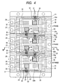
- composition of practical inverter bridge circuit that is, composition of semiconductor module is explained hereinafter.
- the reference number 20 in FIG. 3 and FIG. 4 indicates a heat radiation plate made of oxygen free copper plated with nickel.
- the heat radiation plate 20 is heat conductive, and cooled with cooling medium such as air, water, anti-freeze liquid, and the like.
- a circumference wall of the case 21, of which top and bottom are open, is provided at peripheral portion of the heat radiation plate 20.
- the case 21 is fabricated with a resin having insulating property, and the like. Inner portion of the case is partitioned corresponding to each of the arm in the bridge circuit.
- a pair of the direct current positive pole terminal 26 and the direct current negative pole terminal 27 is provided onto one of side walls, which are facing each other, of the case 21 by insert-fabrication.
- the direct current positive pole terminal 26 and the direct current negative pole terminal 27 are formed from an electrically conductive plate member; one of which is exposed outside from the outer surface of one of the mutually facing side walls of the case 21, and another one is exposed to inner portion of the case 21 by extending through inner portion of one of the mutually facing side walls, which forms a stepwise shape.
- the alternate current terminal 24 is provided into each of the partitions of another one of the mutually facing side walls of the case 21 by insert-fabrication.
- the alternate current terminal 24 is formed from an electrically conductive plate member; one of which is exposed outside from the outer surface of one of the mutually facing side walls of the case 21, and another one is exposed to inner portion of the case 21 by extending through inner portion of one of the mutually facing side walls, which forms a stepwise shape.
- the insulation substrate 22 is provided at each of the partitions on the heat radiation plate 20 in the case 21.
- the insulation substrate 22 is made of ceramics, and conductive patterns 22a, 22b are formed on its both sides bymetallizing.
- the conductive pattern 22b is adhered onto the heat radiation plate 20 with electrically conductive adhesive sheet 29. Accordingly, the conductive pattern 22b is bonded thermally to the heat radiation plate 23.
- the power semiconductor element 23 is bonded to the portion of the direct current negative pole terminal 27 of the conductive pattern 22a at each partition in the case 21 with electrically conductive adhesive sheet 28.
- the power semiconductor element 23 is bonded to another portion of the alternate current terminal 24 of the conductive pattern 22a (the portion is located on a diagonal line from the portion of the direct current negative pole terminal 27 of the conductive pattern 22a) with electrically conductive adhesive sheet 28. Accordingly, the power semiconductor element 23 is bonded electrically and thermally to the conductive pattern 22a. Practical composition of the electrically conductive adhesive sheet 28, 29 will be explained later.
- Each of the power semiconductor element 23 located on the position of the direct current negative pole terminal 27 of the conductive pattern 22a and the direct current negative pole terminal 27, the alternate current terminal 24 and one of the conductive patterns 22a, the power semiconductor element 23 located on the position of another alternate current terminal 24 of the conductive pattern 22a and the alternate current terminal 24, another one of the conductive patterns 22a and the direct current pole terminal 26 are bonded each other with the electrically conductive adhesive sheet 30.
- Practical composition of the electrically conductive adhesive sheet 30 will be explained later.
- the power semiconductor element is shaped in a chip, which is provided with the source electrode 23c and the gate electrode 23b on the upper surface of the chip and the drain electrode on the lower surface of the chip.
- the power semiconductor element 23 located on the portion of the alternate current terminal 24 of the conductive pattern 22a corresponds to the upper arm side element, and the power semiconductor element 23 located on the portion of the direct current negative pole terminal 27 of the conductive pattern 22a corresponds to the lower arm side element.
- the gate electrode 23b is connected electrically to the driving circuit substrate connecting terminal 31 , which is bonded to a substrate composing an inverter driving circuit, which is not shown in the figure, with the wire 32.
- the driving circuit substrate connecting terminal 31 is a member made of conductive material formed a L-shape, one of the ends is exposed in the case, and another end extends upwards through inner portion of the case 21.
- One side of the driving circuit substrate connecting terminal 31 is formed in a flat plane which makes the wire 31 possible to form wire-bonding.
- Another side of the driving circuit substrate connecting terminal 31 is formed in a pin shape which can be inserted into a hole provided to the substrate composing the inverter driving circuit, which is not shown in the figure,
- the driving circuit substrate connecting terminal 31 is provided to the case by insert-fabrication.
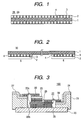
- the reference number 1 in FIG. 1 and FIG. 2 indicates a substrate.
- the substrate is composed of metallic foil, which forms electrically, thermally, or both electrically and thermally conductive paths in a direction along the plane of the sheet.
- the metallic foil is composed of a composite material manufactured by laminating second metallic materials onto both sides of a first metallic material; the metal foil has a coefficient of thermal expansion larger than the coefficient of thermal expansion of the power semiconductor element (2 ⁇ 4 ⁇ 10 -6 /K), which is one of the bonded members, and smaller than the coefficient of thermal expansion of the conductive pattern 22a (17 ⁇ 25 ⁇ 10 -6 /K), which is another one of the bonded members. That is, the coefficient of thermal expansion of the substrate 1 is in intermediate of the coefficients of thermal expansion of the bonded members.
- the first metallic material has a coefficient of thermal expansion smaller than the coefficient of thermal expansion of the second metallic material.
- an iron-nickel alloy of 35 ⁇ m thick containing nickel 42% by weight is used as the first metallic material.
- an example using the iron-nickel alloy containing nickel 42% by weight is explained.
- the present invention is not restricted by this example, and the content of nickel is preferably in the range of 30 ⁇ 55% by weight.
- the second metallic material has a volume resistivity smaller than the volume resistivity of the first metallic material.
- a copper foil of approximately 10 ⁇ m thick is used as the second metallic material, and the both sides of the iron-nickel alloy plate are clad with the copper foil.
- total thickness of the substrate 1 becomes 55 ⁇ m, but the present invention is not restricted by this example, and the total thickness of the substrate 1 may preferably be set in the range of several ⁇ m to several mm.
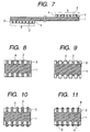
- a protrusion layer 2 is formed on both sides of the substrate of the electrically conductive adhesive sheet 28, 29 shown in FIG. 1, and on one side of the substrate, which is connecting portion 5 facing to the bonded member (in accordance with the present embodiment, both ends of the substrate), of the electrically conductive adhesive sheet 30 shown in FIG. 2.
- plural metallic columns 3 are formed on the surface of the substrate 1 in a matrix arrangement with an equal pitch of 200 ⁇ m, and it forms electrically, thermally, or both electrically and thermally conductive paths between the substrate 1 and the bonded member, that is, in a direction along the thickness of the sheet.
- the metallic column 3 is a short cylinder having a circular cross section, which is 100 ⁇ m in diameter and 50 ⁇ m in length in a direction along the thickness of the sheet, and the metallic column 3 is provided on the surface of the substrate so that top of the column is exposed outside from the resin composition 4 or so that top of the column is extended outside of the resin composition 4.
- the resin composition 4 is filled into the vacancy among plural metallic columns 3 in the protrusion layer 2.
- the resin composition 4 is 50 ⁇ m thick in a direction along the thickness of the sheet, and it is made of thermosetting polyimide film.
- the resin composition is filled into only the bonding portion 5 where the protrusion layer 2 is formed.
- an insulation resin layer may be formed onto a portion other than the bonding portion and surface of the substrate 1 with the aim of ensuring insulation from other circuits.
- the resin to form the insulation resin layer may be the same resin as the resin composition 4 or other different resin from the resin composition 4.
- top of the metallic column 3 is exposed outside from the surface of the resin composition 4 or extended outside from outside of the surface of the resin composition 4, as described previously, but there are various methods to realize this matter, and any method may be used.
- the top of the metallic column 3 may be placed at the same level as the surface of the resin composition 4.
- top of the metallic column is placed at a lower level than the surface of the resin composition 4, and dimples may be formed on the surface of the resin composition 4.
- top of the metallic column is placed at a higher level than the surface of the resin composition 4, and the top of the metallic column 3 may be exposed outside from the surface of the resin composition 4 .
- the method to form dimples onto the surface of the resin composition 4 as shown in FIG. 9 may be advantageous.
- the method to extend the top of the metallic column 3 outside from the surface of the resin composition 4 as shown in FIG. 10 can be said as advantageous.
- a short cylinder having a circular cross section was used as the metallic column as mentioned previously, but the column may have a polygonal cross section.
- the metallic columns were arranged regularly in a matrix with a pitch as mentioned previously, but irregular arrangement is adoptable.
- the thickness of the protrusion layer 2 was set as 50 ⁇ m as mentioned previously, but the thickness is not limited by the present embodiment, and the thickness of the protrusion layer 2 may be set within a range of several microns to several millimeters.
- polyimide film was used as the resin composition 4, as mentioned previously, but resins, of which main component is a thermosetting resins such as epoxy resin, phenol resin, and the like, may be useful. Or, resins, of which main component is a thermoplastic resin such as polyamide resin, polyamide-imide resin, polyether-imide resin, and the like, may be useful as the resin composition 4. Or, a mixture of thermosetting resin and thermoplastic resin may be useful as the resin composition 4. A filler such as inorganic filler, glass, and the like may be mixed into the resin composition 4.
- the electrically conductive adhesive sheet 28, 29 shown in FIG. 1 of the present embodiment is usable for bonding two bonding members, of which bonding planes are facing each other in a direction along the thickness direction of the sheet such as connection between the power semiconductor element 23 and the conductive pattern 22a, and connection between the conductive pattern 22b and the heat radiation plate 20.
- the electrically conductive adhesive sheet 30 shown in FIG. 2 of the present embodiment is usable for connecting two bonding members, of which bonding planes are facing in a same direction at a different position each other of a plane in a direction along the plane of the sheet such as connection between the conductive pattern 22a and the direct current positive pole terminal 26 or the alternate current terminal 24, and connection between the power semiconductor element 23 and the direct current negative pole terminal 27 or the alternate current terminal 24.
- one of the protrusion layer 2 provided at both ends of one side of the substrate 1 of the electrically conductive adhesive sheet 30 shown in FIG. 2 is further provided at one end of another side of the substrate 1 as shown in FIG. 7, that is, the electrically conductive adhesive sheet may be formed in a crank-shape.
- the manufacturing method of the electrically conductive adhesive sheet 28, 29 shown in FIG. 1 is taken as an example for the explanation, but this manufacturing method is applicable to the electrically conductive adhesive sheet 30 shown in FIG. 2 in the same manner.
- Both sides of iron-nickel alloy foil (made by Hitachi Metal Co. :YEF42) containing nickel 42% by weight of 35 ⁇ m thick are electroplated with copper. Accordingly, the substrate 1 made of iron-nickel alloy foil, both sides of which is clad with copper of approximately 10 ⁇ m thick, is manufactured.
- polyimide film made by Ube Kosan Co. :UPILEX VT
- a sheet member which is composed of the substrate 1 having a resin layer made of the resin composition 4 on both sides is manufactured.
- Holes of 100 ⁇ m in diameter are formed into all the surface of the resin layer on both sides of the sheet member in directions of length and width with an equal pitch of 200 ⁇ m using a UV-YAG type laser boring machine.
- the protrusion layer 2 in which top of the metallic column 3 is exposed outside from the surface of the resin composition 4, or top of the metallic column 3 is extended outside from the surface of the resin composition 4, is manufactured, and electrically conductive adhesive sheet of approximately 150 ⁇ m thick is obtained.
- the protrusion layer 2 was formed by electroplating with copper as mentioned previously, but the present invention is not restricted with this method.
- Various methods such as a method of etching a part of the substrate 1, a method of sputtering a same or different kind of metal onto the surface of the substrate 1, a method of cladding a same or different kind of metal onto the surface of the substrate 1, are applicable.
- a case 21 in which a heat radiation plate 20, an insulation substrate 22 having metallized conductive pattern 22a , 22b on both sides, a direct current positive pole terminal 26, a direct current negative pole terminal 27, an alternate current terminal 24, and a driving circuit substrate connecting terminal 31 are inserted, and power semiconductor elements 23 are prepared.
- the electrically conductive adhesive sheet 29 shown in FIG. 1 is placed onto the heat radiation plate 20, and the insulation substrate 22 is placed onto the electrically conductive adhesive sheet 29 so that the conductive pattern 22b faces downwards. Furthermore, the electrically conductive adhesive sheet 28 shown in FIG. 1 is placed onto the insulation substrate 22 at each of the portions on the one side of the conductive pattern 22a and the direct current negative pole terminal 27 side and on another side of the conductive pattern 22a and the alternate current terminal 24; and the power semiconductor element 23 is placed onto each of the electrically conductive adhesive sheets 28 so that the plane of the drain electrode faces downwards. Under this condition, the piled up members are thermally bonded with pressure by vacuum pressing machine.
- the resin composition 4 is cured or molten, and the resin composition 4 and the bonding members are bonded in a condition that the surface of the metallic column is contacted with the surface of the bonding members with plane-plane contact, and the bonding members are bonded.
- the top of the metallic column 3 and the bonded member can be welded by applying ultrasonic wave to a metal at the top of the metallic column and a metal at the bonded member for melting-adhesion during the bonding process. Accordingly, a strong connecting strength can be obtained.
- the heat radiation plate 20 is adhered to the case 21 with a silicone adhesive agent (not shown in the figure) .
- the protrusion layer 2 on the one side of the electrically conductive adhesive sheet 30 shown in FIG. 2 is placed onto the plane of the source electrode 23c of the power semiconductor element 23, the protrusion layer 2 on another side is placed onto the plane of the direct current negative pole terminal 27, and these members are bonded by a flip chip bonder.
- the protrusion layer 2 on the one side of the electrically conductive adhesive sheet 30 shown in FIG. 2 is placed onto the plane of the source electrode 23c of the power semiconductor element 23, the protrusion layer 2 on another side is placed onto the plane of the alternate current terminal 24, and these members are bonded by a flip chip bonder.
- the protrusion layer 2 on another side is placed onto the plane of the direct current positive pole terminal 6, and these members are bonded by a flip chip bonder.
- the protrusion layer 2 on the one side of the electrically conductive adhesive sheet 30 shown in FIG. 2 is placed onto the plane of the conductive pattern 22a, the protrusion layer 2 on another side is placed onto the plane of the alternate current terminal 24, and these members are bonded by a flip chip bonder.
- the gate electrode 23b of the power semiconductor element 23 and the driving circuit substrate connecting terminal 31 are bonded with wire 32 to connect the gate electrode 23b of the power semiconductor element 23 with the driving circuit substrate connecting terminal 31 electrically.
- Silicone gel resin (not shown in the figure) is poured into the case 21, and a cover made of resin (not shown in the figure) is adhered onto the upper opening of the case 21 with an epoxy resin adhesive agent (not shown in the figure) to close the upper opening of the case 21 with the cover made of resin (not shown in the figure).
- the electrically conductive adhesive sheet of the present embodiment because metallic foil made of a composite material which is composed of a metal having s small volume resistivity and a metal having a small coefficient of thermal expansion is used as the substrate 1, the volume resistivity of the substrate 1 can be made small as equivalent as conventional metal substrate made of copper, and concurrently, the coefficient of thermal expansion of the substrate 1 can be made smaller than that of conventional metal substrate made of copper. Therefore, the electrically conductive adhesive sheet of the present embodiment can moderate the stress applied to the metallic column 3 owing to the difference in thermal expansion corresponding to the difference in coefficient of thermal expansion of bonded members, for instance, the power semiconductor element 23 and the conductive pattern 22a, and connection reliability can be improved better than ever.
- the electrically conductive adhesive sheet of the present embodiment even if the electrically conductive adhesive sheet is applied as the bonding member to an equipment which is operated under severe thermal cycles, for instance, an electric power conversion equipment for vehicle which is required to have a long product life over than 15 years, the equipment can maintain the connection reliability for a long time, and the electrically conductive adhesive sheet can contribute to long extension of the product life of the equipment. Furthermore, in the present embodiment, a composite material was used as the substrate 1, but if any single material having a low volume resistivity and a low coefficient of thermal expansion as equivalent to the composite material is available, the single material can be used as the substrate 1. If the electrically conductive adhesive sheet is used as a bonding member aiming only at thermal connection of the bonded member, an iron-nickel alloy containing nickel 30 ⁇ 55 % by weight can be used as a single material for the substrate 1.
- the protrusion layer 2 and the substrate 1 form thermal and electrical conducting paths, and no contact point is formed inside the sheet. Therefore, the same thermal conductivity and volume resistivity as metal can be obtained.
- the metallic column 3 can readily be deformed elastically, because the resin composition is filled into the protrusion layer 2. Therefore, in accordance with the electrically conductive adhesive sheet of the present embodiment, the stress generated at bonded boundary plane of the bonded members, for instance, the power semiconductor 23 and the conductive pattern 22a, on account of the difference in thermal expansion corresponding to the difference in their coefficients of thermal expansion, the stress generated at the bonded boundary plane of the power semiconductor element 23 and the electrically conductive adhesive sheet, and the stress generated at the bonded boundary plane of the conductive pattern 22 and the electrically conductive adhesive sheet, can be moderated.
- the inventor cut the electrically conductive adhesive sheet obtained in the present embodiment to a sheet of 10 mm X 10 mm, and measured its thermal resistance and electric resistance.
- the thermal resistance of the electrically conductive adhesive sheet obtained in the present embodiment was 0.019 (K/W), and electric resistance was 9.2 X 10 -8 ( ⁇ ).
- a temperature cycle test under an environment of low temperature of -40 °C for 30 minutes and high temperature of 125 °C for 30 minutes was performed for 1000 cycles on the power conversion equipment for vehicle, in which the electrically conductive adhesive sheet of the present embodiment was applied as a bonding member. After the temperature cycle test, the cross section of the sample was observed. As the result, any failure such as wire breakage, peeling, and the like was not observed, and high reliability of the power conversion equipment for vehicle, in which the electrically conductive adhesive sheet of the present embodiment was applied, was confirmed.
- a method of manufacturing the electrically conductive adhesive sheet which is the embodiment 2 of the present invention, is explained hereinafter.
- the composition of the electrically conductive adhesive sheet of the present embodiment is as same as the composition of the electrically conductive adhesive sheet of the embodiment 1.
- the present embodiment is explained on the manufacturing method of the electrically conductive adhesive sheet having the same structure as the embodiment 1 for example, in which the protrusion layer 2 is provided on both sides of the substrate 1, but the method is applicable to the structure, in which the protrusion layer 2 is provided only on one side of the substrate 1.
- Both sides of iron-nickel alloy foil (made by Hitachi Metal Co. : YEF42) containing Nickel 42% by weight of 35 ⁇ m thick are electroplated with copper. Accordingly, the substrate 1 made of iron-nickel alloy foil, both sides of which is clad with copper of approximately 10 ⁇ m thick, is manufactured.
- Both sides of the substrate is laminated with photosensitive resist to be approximately 50 ⁇ m thick, focused with photo-mask, and exposed to light with extra-high pressure mercury lamp. Then, holes of 100 ⁇ m in diameter are formed into all the surface of the photosensitive resist on both sides of the substrate 1 in the directions of length and width with an equal pitch of 200 ⁇ m by development.
- Polyimide varnish (made by Ube Kosan Co. : U-Varnish-A) is printed on the protrusion layer 2 formed on both sides of the substrate 1 using metal mask, and it is dried at 130 °C in an oven for 30 minutes. Accordingly, the resin composition 4 is filled into the protrusion layer 2.
- the electrically conductive adhesive sheet of approximately 150 ⁇ m thick was manufactured by removing residual of the polyimide varnish at edge of the protrusion layer 2 by plasma washer, and extending or exposing top of the metallic column 3 outside from the surface of the resin composition 4.
- a method of manufacturing the electrically conductive adhesive sheet which is the embodiment 3 of the present invention, is explained hereinafter.
- the composition of the electrically conductive adhesive sheet of the present embodiment is as same as the composition of the electrically conductive adhesive sheet of the embodiment 1.
- the present embodiment is explained on the manufacturing method of the electrically conductive adhesive sheet having the same structure as the embodiment 1 for example, in which the protrusion layer 2 is provided on both sides of the substrate 1, but the method is applicable to the structure, in which the protrusion layer is provided only on one side of the substrate 1.
- Both sides of iron-nickel alloy foil (made by Hitachi Metal Co.: YEF42) containing Nickel 42% by weight of 35 ⁇ m thick are electroplated with copper. Accordingly, the substrate 1 made of iron-nickel alloy foil, both sides of which is clad with copper of approximately 10 ⁇ m thick, is manufactured.
- a sheet member which is composed of the substrate 1 having a resin layer of the resin composition 4 on both sides, is manufactured by laminating both sides of the substrate with epoxy group insulation resin(made by Asahi Denka Co.: BUR-453S) to be approximately 50 ⁇ m thick, and heating and curing with vacuum pressing machine.
- epoxy group insulation resin made by Asahi Denka Co.: BUR-453S
- Holes of 100 ⁇ m in diameter are formed into all the surface of the resin layer on both sides of the substrate 1 in the directions of length and width with an equal pitch of 200 ⁇ m by UV-YAG laser boring machine.
- the electrically conductive adhesive sheet of approximately 150 ⁇ m thick is obtained by electroplating the inner side of the holes of the sheet member with copper in order to form the protrusion layer 2, in which top of the metallic column 3 is extended or exposed outside from the surface of the resin composition 4.
- a composition of the electrically conductive adhesive sheet which is the embodiment 4 of the present invention, is explained hereinafter referring to FIG. 11.
- the electrically conductive adhesive sheet of the present embodiment is manufactured by any one of the manufacturing methods explained in the embodiments 1 to 3, and a metallic layer 6 made of nickel and gold is formed at the top of the metallic column 3 composing the protrusion layer 2.
- the electrically conductive adhesive sheet of the present embodiment composed of as explained above, is obtained by manufacturing the electrically conductive adhesive sheet by any one of the manufacturing methods explained in the embodiments 1 to 3, and electroless plating the top of the metallic column 3, which composes the protrusion layer 2, with nickel to approximately 5 ⁇ m thick, then, electroless plating the top of the metallic column with gold further to form the metallic layer 6 made of nickel and gold at the top of the metallic column 3 which composes the protrusion layer 2.
- the contact resistance at the surface of the bonded members, for instance, at the surface of the power semiconductor element 23 and the top of the metallic layer 6 can be made smaller than any of the electrically conductive adhesive sheet of the embodiments 1 to 3, and thermal conductivity and volume resistivity can be improved further.
- the metallic layer 6 was formed by plating, but the present invention is not restricted with this example, and other manufacturing methods such as sputtering, cladding, and the like are applicable.
- the present embodiment is explained on the case that the metallic layer 6 is formed at the top of the metallic column 3 made of copper.
- the metallic column 3 is made of iron-nickel alloy, plating with copper is performed first, and then, electroless nickel plating and electroless gold plating are performed.
- a gold plated layer can be provided at the outermost layer of the top of the metallic column 3, and the contact resistance between bonded members, for instance, the contact resistance between the surface of power semiconductor element 23 and the top of the metallic layer 6 can be made small.
- the metallic column 3 is made of a metal other than aluminum
- aluminum is provided at the top of the metallic column 3 by sputtering, and ultrasonic wave is applied in a pressurizing-heating process for bonding the bonding members, for instance, bonding the power semiconductor element 23 and the electrically conductive adhesive sheet, welding of aluminum pad of the power semiconductor element 23 to the top of the metallic column 3 can be performed favorably, and a high bonding strength can be obtained.
- the electrically conductive adhesive sheet which is the embodiment 5 of the present invention, is explained hereinafter.
- the electrically conductive adhesive sheet of the present embodiment is manufactured by any one of the manufacturing methods explained in the embodiments 1 to 3, and a metallic layer 6 made of tin is formed at the top of the metallic column 3 composing the protrusion layer 2.
- the electrically conductive adhesive sheet of the present embodiment composed of as explained above, is obtained by manufacturing the electrically conductive adhesive sheet by any one of the manufacturing methods explained in the embodiments 1 to 3, and electroplating the top of the metallic column 3, which composes the protrusion layer 2, with a tin- zinc alloy to approximately 10 ⁇ m thick to form the metallic layer 6 made of the tin-zinc alloy at the top of the metallic column 3 which composes the protrusion layer 2.
- the present embodiment is explained on the case that the metallic layer 6 made of the tin-zinc alloy is formed at the top of the metallic column 3 made of copper, but another metallic layer 6 which is made of electroless tin and silver may be formed instead at the top of the metallic column 3. That is, electroless plating the top of the metallic column 3 with tin, and then, plating the top of the metallic column 3 with silver to form the metallic layer 6 at the top of the metallic column 3.
- the metallic layer 6 composed of the electroless tin and silver is molten, and the top of the metallic column 3 can be soldered to a metallic plane of the bonding member. Accordingly, a high bonding strength can be obtained.
Landscapes
- Engineering & Computer Science (AREA)
- Chemical & Material Sciences (AREA)
- Combustion & Propulsion (AREA)
- Transportation (AREA)
- Mechanical Engineering (AREA)
- Manufacturing & Machinery (AREA)
- Microelectronics & Electronic Packaging (AREA)
- Cooling Or The Like Of Semiconductors Or Solid State Devices (AREA)
- Inverter Devices (AREA)
- Adhesive Tapes (AREA)
- Adhesives Or Adhesive Processes (AREA)
Applications Claiming Priority (2)
| Application Number | Priority Date | Filing Date | Title |
|---|---|---|---|
| JP2004000734A JP4192786B2 (ja) | 2004-01-06 | 2004-01-06 | 導電性接着シート及びその製造方法並びに電力変換装置 |
| JP2004000734 | 2004-01-06 |
Publications (2)
| Publication Number | Publication Date |
|---|---|
| EP1553629A2 true EP1553629A2 (fr) | 2005-07-13 |
| EP1553629A3 EP1553629A3 (fr) | 2007-11-14 |
Family
ID=34587659
Family Applications (1)
| Application Number | Title | Priority Date | Filing Date |
|---|---|---|---|
| EP05000127A Withdrawn EP1553629A3 (fr) | 2004-01-06 | 2005-01-05 | Feuille adhésive conducteur électrique, méthode de fabrication associée et convertisseur électrique à haute prestation |
Country Status (3)
| Country | Link |
|---|---|
| US (1) | US20050147839A1 (fr) |
| EP (1) | EP1553629A3 (fr) |
| JP (1) | JP4192786B2 (fr) |
Families Citing this family (10)
| Publication number | Priority date | Publication date | Assignee | Title |
|---|---|---|---|---|
| JP2006196853A (ja) * | 2004-12-13 | 2006-07-27 | Daikin Ind Ltd | ヒートポンプ装置 |
| JP4359250B2 (ja) | 2005-02-10 | 2009-11-04 | 株式会社日立製作所 | インターフェース回路及び電力変換装置並びに車載用電機システム |
| US8871355B1 (en) * | 2010-10-08 | 2014-10-28 | Clemson University | Microstructure enhanced sinter bonding of metal injection molded part to a support substrate |
| JP2014183256A (ja) * | 2013-03-21 | 2014-09-29 | Denso Corp | 接合体およびこれを用いた半導体装置、ならびにそれらの製造方法 |
| DE102015213085A1 (de) * | 2015-07-13 | 2016-06-16 | Siemens Aktiengesellschaft | Leistungsmodul sowie Verfahren zum Herstellen eines Leistungsmoduls |
| DE102017101582A1 (de) * | 2017-01-26 | 2018-07-26 | Bombardier Primove Gmbh | Empfangsvorrichtung und Verfahren zur Herstellung |
| DE102018203065A1 (de) * | 2018-03-01 | 2019-09-05 | Robert Bosch Gmbh | Verfahren zur Herstellung eines Injektors |
| CN209845450U (zh) * | 2019-04-26 | 2019-12-24 | 宁德时代新能源科技股份有限公司 | 一种电池模组 |
| JP2025090142A (ja) * | 2023-12-05 | 2025-06-17 | デクセリアルズ株式会社 | 熱伝導シート、及び熱伝導シートの製造方法 |
| WO2026058647A1 (fr) * | 2024-09-12 | 2026-03-19 | デクセリアルズ株式会社 | Procédé de fabrication de stratifié et stratifié |
Family Cites Families (5)
| Publication number | Priority date | Publication date | Assignee | Title |
|---|---|---|---|---|
| US5653379A (en) * | 1989-12-18 | 1997-08-05 | Texas Instruments Incorporated | Clad metal substrate |
| US5065227A (en) * | 1990-06-04 | 1991-11-12 | International Business Machines Corporation | Integrated circuit packaging using flexible substrate |
| US6373348B1 (en) * | 2000-08-11 | 2002-04-16 | Tektronix, Inc. | High speed differential attenuator using a low temperature co-fired ceramic substrate |
| WO2002082543A1 (fr) * | 2001-03-30 | 2002-10-17 | Hitachi, Ltd. | Dispositif a semi-conducteur |
| US20030127727A1 (en) * | 2002-01-09 | 2003-07-10 | Nitto Denko Corporation | Thermally conductive sheet and semiconductor device using same |
-
2004
- 2004-01-06 JP JP2004000734A patent/JP4192786B2/ja not_active Expired - Fee Related
-
2005
- 2005-01-05 US US11/028,582 patent/US20050147839A1/en not_active Abandoned
- 2005-01-05 EP EP05000127A patent/EP1553629A3/fr not_active Withdrawn
Also Published As
| Publication number | Publication date |
|---|---|
| EP1553629A3 (fr) | 2007-11-14 |
| US20050147839A1 (en) | 2005-07-07 |
| JP4192786B2 (ja) | 2008-12-10 |
| JP2005197377A (ja) | 2005-07-21 |
Similar Documents
| Publication | Publication Date | Title |
|---|---|---|
| US9439332B2 (en) | Power module | |
| CN100539308C (zh) | 电子装置 | |
| US9033207B2 (en) | Method of manufacturing electronic component unit | |
| US11631623B2 (en) | Power semiconductor device and method of manufacturing the same, and power conversion device | |
| US20190393799A1 (en) | Power Module, Power Converter Device, and Electrically Powered Vehicle | |
| US9591789B2 (en) | Power semiconductor module and power module | |
| JP6797285B2 (ja) | 半導体装置およびその製造方法、ならびに電力変換装置 | |
| US20070163765A1 (en) | Power-electronic-cooling device | |
| US20090237890A1 (en) | Semiconductor device and method for manufacturing the same | |
| EP1553629A2 (fr) | Feuille adhésive conducteur électrique, méthode de fabrication associée et convertisseur électrique à haute prestation | |
| US8531067B2 (en) | Alternator with synchronous rectification equipped with an improved electronic power module | |
| WO2016121443A1 (fr) | Dispositif électronique | |
| JP7760399B2 (ja) | 半導体装置 | |
| JP6344981B2 (ja) | 半導体モジュールの製造方法 | |
| US7518236B2 (en) | Power circuit package and fabrication method | |
| JP7237214B2 (ja) | 半導体パワーモジュールのための金属基板構造および金属基板構造の製造方法ならびに半導体パワーモジュール | |
| JP4961314B2 (ja) | パワー半導体装置 | |
| US20110127863A1 (en) | Alternator with synchronous rectification equipped with an improved electronic power module | |
| JP2013122993A (ja) | 半導体装置 | |
| JPH0323828Y2 (fr) | ||
| WO2022210617A1 (fr) | Dispositif à semi-conducteur et système à semi-conducteur | |
| CN120998910A (zh) | 一种半导体模组、集成模块、控制器及车辆 | |
| CN118075976A (zh) | 散热模组及散热模组的制备方法 | |
| WO2025203906A1 (fr) | Dispositif à semi-conducteur de puissance et procédé de fabrication d'un dispositif à semi-conducteur de puissance | |
| WO2022249805A1 (fr) | Dispositif à semi-conducteur |
Legal Events
| Date | Code | Title | Description |
|---|---|---|---|
| PUAI | Public reference made under article 153(3) epc to a published international application that has entered the european phase |
Free format text: ORIGINAL CODE: 0009012 |
|
| AK | Designated contracting states |
Kind code of ref document: A2 Designated state(s): AT BE BG CH CY CZ DE DK EE ES FI FR GB GR HU IE IS IT LI LT LU MC NL PL PT RO SE SI SK TR |
|
| AX | Request for extension of the european patent |
Extension state: AL BA HR LV MK YU |
|
| PUAL | Search report despatched |
Free format text: ORIGINAL CODE: 0009013 |
|
| AK | Designated contracting states |
Kind code of ref document: A3 Designated state(s): AT BE BG CH CY CZ DE DK EE ES FI FR GB GR HU IE IS IT LI LT LU MC NL PL PT RO SE SI SK TR |
|
| AX | Request for extension of the european patent |
Extension state: AL BA HR LV MK YU |
|
| AKX | Designation fees paid |
Designated state(s): DE |
|
| STAA | Information on the status of an ep patent application or granted ep patent |
Free format text: STATUS: THE APPLICATION IS DEEMED TO BE WITHDRAWN |
|
| 18D | Application deemed to be withdrawn |
Effective date: 20080515 |