EP1553676A1 - Elektronisches Schutzgerät - Google Patents
Elektronisches Schutzgerät Download PDFInfo
- Publication number
- EP1553676A1 EP1553676A1 EP04290064A EP04290064A EP1553676A1 EP 1553676 A1 EP1553676 A1 EP 1553676A1 EP 04290064 A EP04290064 A EP 04290064A EP 04290064 A EP04290064 A EP 04290064A EP 1553676 A1 EP1553676 A1 EP 1553676A1
- Authority
- EP
- European Patent Office
- Prior art keywords
- output
- threshold voltage
- protection device
- electronic protection
- input signal
- Prior art date
- Legal status (The legal status is an assumption and is not a legal conclusion. Google has not performed a legal analysis and makes no representation as to the accuracy of the status listed.)
- Withdrawn
Links
Images


Classifications
-
- G—PHYSICS
- G06—COMPUTING OR CALCULATING; COUNTING
- G06F—ELECTRIC DIGITAL DATA PROCESSING
- G06F1/00—Details not covered by groups G06F3/00 - G06F13/00 and G06F21/00
- G06F1/26—Power supply means, e.g. regulation thereof
- G06F1/30—Means for acting in the event of power-supply failure or interruption, e.g. power-supply fluctuations
Definitions
- the invention relates to an electronic protection device.
- FIG. 1 illustrates one example of electronic circuit that may suffer potential damage on slowly changing power supply.
- Block 10 is the digital circuitry that drives a transistor 11 .
- the transistor is biased by a biasing supply V CC .
- V CC biasing supply
- the V CC supply transits between 0.8 to 1.5 volts, while the output supply is present a reverse current flows from the collector to the driving circuitry through the base of the transistor this current can cause damage to the driving circuitry and/or port pins toggling, therefore is not desirable.
- Another example relates to general-purpose micro controllers such as the product sold under the name "ST7" by the Applicant and which is operated from a supply voltage of 5V.
- ST7 general-purpose micro controllers
- the LVD (low voltage detector) feature on the ST7 is intended to keep all the I/O lines at RESET level until V DD reaches V DDmin (typically 3.8 volts).
- V DDmin typically 3.8 volts.
- V DDmin typically 3.8 volts
- LVD loses its control on the I/O lines causing them to toggle. This undesired toggling can result in severe problems in power applications, such as when the I/O port drives the BJT/MOSFET.
- Object of the invention is to provide a method and device to obviate the drawbacks from the prior art and provide reliable protection of digital circuits with respect to changing voltage level.
- this invention provides an electronic protection device that disables the output from a digital circuit whenever an input signal is below a threshold voltage level, comprising:
- the said threshold voltage detector comprises a plurality of diodes connected in series.
- the said gating means is a controlled switch.
- the said threshold voltage sensor is a zener diode or micro controller.
- the said digital circuit is a microcontroller.
- the said microcontroller includes a mechanism for delaying the digital output for a predefined period after the input signal has attained the defined threshold level.
- the said mechanism is a software means.
- the instant invention also provides a method for disabling the output from a digital circuit whenever an input signal is below a threshold voltage level, comprising the steps of:
- the gating is implementing using standard logic gates.
- the above method further includes the step of delaying the digital output for a predefined period after the input signal has attained the defined threshold level.
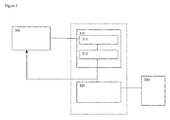
- FIG. 2 shows a block diagram for a proffered embodiment in accordance with the present invention.
- Block 200 is a driving circuit and block 230 is the load.
- the blocks 210 and 220 together constitute the protection device of the invention.
- Block 210 is a voltage-monitor, comprising a voltage detecting element 211 receiving input from the driving circuit 200 and providing it to controlling gate 212 .
- the output of block 210 is connected to switching element 230 .
- the voltage-detecting element 211 receives input from the driving circuit 200 and enables gate 212 only when the voltage is above a defined threshold limit.
- Gate 212 enables switching element 230 that enables the driving circuit 200 to drive the load.
- Block 300 is a general-purpose micro controller.
- Micro controller 300 is connected to load 330 through the protecting device comprising blocks 310 and 320 .
- Block 310 contains a voltage threshold detector 311 that provides input to gate 312 .
- the output of the gate is connected to the switching element 330 and is also provided to the micro controller.
- the switch is enabled on receipt of the signal from the gate but the signal from the micro controller is passed to the switch 330 only once a predetermined period of time is elapsed after the receipt of signal from the gate 312 .
- the software residing inside the micro controller for this purpose computes the predetermined time.
- Figure 4 shows a particular embodiment of the invention wherein the threshold conducting means is realized by a series of diodes and the gate is a simple NAND gate.
- the operation of this circuit can be understood as follows.
- the Micro-controller Unit is an ST7 that generates a PWM output to drive the transistor which operates the load.
- the micro controller suffers from the problem of toggling I/Os when the supply voltage is in the 0.8 - 1.5 volts range.
- the LVD circuit loses its control over the I/O line and fails to keep the I/O at the RESET level. While the micro controller pin toggles, the MCU can generate a PWM sufficient to drive the transistor. The present invention protects this by not allowing micro controller to drive the transistor when the power supply is transitioning.
- the series connected diodes block the micro controller's output signal when until the supply crosses the range of 0.8 - 1.5 volts.
- the number of diodes that are connected in series are selected according to the voltage levels required.
- a software is further provided with the micro controller, that disables the signal from the micro controller before it is passed to the AND gate to drive the load until a predetermined period of time is elapsed after the receipt of the signal from the AND gate.
- the predetermined time is computed by software residing inside the micro controller for this purpose.
Landscapes
- Engineering & Computer Science (AREA)
- Theoretical Computer Science (AREA)
- Physics & Mathematics (AREA)
- General Engineering & Computer Science (AREA)
- General Physics & Mathematics (AREA)
- Emergency Protection Circuit Devices (AREA)
Priority Applications (1)
| Application Number | Priority Date | Filing Date | Title |
|---|---|---|---|
| EP04290064A EP1553676A1 (de) | 2004-01-09 | 2004-01-09 | Elektronisches Schutzgerät |
Applications Claiming Priority (1)
| Application Number | Priority Date | Filing Date | Title |
|---|---|---|---|
| EP04290064A EP1553676A1 (de) | 2004-01-09 | 2004-01-09 | Elektronisches Schutzgerät |
Publications (1)
| Publication Number | Publication Date |
|---|---|
| EP1553676A1 true EP1553676A1 (de) | 2005-07-13 |
Family
ID=34586019
Family Applications (1)
| Application Number | Title | Priority Date | Filing Date |
|---|---|---|---|
| EP04290064A Withdrawn EP1553676A1 (de) | 2004-01-09 | 2004-01-09 | Elektronisches Schutzgerät |
Country Status (1)
| Country | Link |
|---|---|
| EP (1) | EP1553676A1 (de) |
Cited By (2)
| Publication number | Priority date | Publication date | Assignee | Title |
|---|---|---|---|---|
| US7921059B2 (en) | 2005-12-15 | 2011-04-05 | Microsoft Corporation | Licensing upsell |
| CN112865769A (zh) * | 2021-01-19 | 2021-05-28 | 珠海拓芯科技有限公司 | 一种驱动电路与电子设备 |
Citations (6)
| Publication number | Priority date | Publication date | Assignee | Title |
|---|---|---|---|---|
| US4493000A (en) * | 1983-09-30 | 1985-01-08 | Magnetic Peripherals Incorporated | Power on/off protect circuit |
| US4843592A (en) * | 1986-04-10 | 1989-06-27 | Kabushiki Kaisha Toshiba | Microcomputer controlled apparatus provided with a battery voltage detection circuit |
| EP0369782A2 (de) * | 1988-11-18 | 1990-05-23 | Seiko Instruments Inc. | Schaltung zum Betrieb eines Gerätes, wie ein Drucker |
| DE4014831A1 (de) * | 1990-05-09 | 1991-12-12 | Standard Elektrik Lorenz Ag | Unterspannungsgeschuetzte schaltungsanordnung |
| DE4200681A1 (de) * | 1992-01-14 | 1993-07-15 | Bosch Gmbh Robert | Schaltungsanordnung zur unterspannungserkennung |
| US6118315A (en) * | 1992-12-22 | 2000-09-12 | Sgs-Thomson Microelectronics S.A. | Power-on-reset circuit providing protection against power supply interruptions |
-
2004
- 2004-01-09 EP EP04290064A patent/EP1553676A1/de not_active Withdrawn
Patent Citations (6)
| Publication number | Priority date | Publication date | Assignee | Title |
|---|---|---|---|---|
| US4493000A (en) * | 1983-09-30 | 1985-01-08 | Magnetic Peripherals Incorporated | Power on/off protect circuit |
| US4843592A (en) * | 1986-04-10 | 1989-06-27 | Kabushiki Kaisha Toshiba | Microcomputer controlled apparatus provided with a battery voltage detection circuit |
| EP0369782A2 (de) * | 1988-11-18 | 1990-05-23 | Seiko Instruments Inc. | Schaltung zum Betrieb eines Gerätes, wie ein Drucker |
| DE4014831A1 (de) * | 1990-05-09 | 1991-12-12 | Standard Elektrik Lorenz Ag | Unterspannungsgeschuetzte schaltungsanordnung |
| DE4200681A1 (de) * | 1992-01-14 | 1993-07-15 | Bosch Gmbh Robert | Schaltungsanordnung zur unterspannungserkennung |
| US6118315A (en) * | 1992-12-22 | 2000-09-12 | Sgs-Thomson Microelectronics S.A. | Power-on-reset circuit providing protection against power supply interruptions |
Cited By (2)
| Publication number | Priority date | Publication date | Assignee | Title |
|---|---|---|---|---|
| US7921059B2 (en) | 2005-12-15 | 2011-04-05 | Microsoft Corporation | Licensing upsell |
| CN112865769A (zh) * | 2021-01-19 | 2021-05-28 | 珠海拓芯科技有限公司 | 一种驱动电路与电子设备 |
Similar Documents
| Publication | Publication Date | Title |
|---|---|---|
| US10110217B2 (en) | Load driving device | |
| US7741820B2 (en) | Switching voltage regulator pulse width modulation controller and method | |
| JP4267865B2 (ja) | 負荷駆動装置 | |
| US4698582A (en) | Power driver having short circuit protection | |
| CN107852159B (zh) | 驱动装置 | |
| US8427804B2 (en) | Power amplifier | |
| US7064946B2 (en) | Electronic fuse | |
| CN101246059B (zh) | 温度检测电路 | |
| US20180026517A1 (en) | Driver circuit, circuit arrangement comprising a driver circuit, and inverter comprising a circuit arrangement | |
| US7768759B2 (en) | Control circuit of semiconductor device having over-heat protecting function | |
| JP2004080346A (ja) | 電流制限回路およびそれを備えた出力回路 | |
| US10931191B2 (en) | Half bridge circuit driver chip with protection circuit and protection method thereof | |
| US10103539B2 (en) | Semiconductor device and current limiting method | |
| EP2079165A2 (de) | Laststeuerungs- und Diagnosesystem und Steuerverfahren | |
| KR101876517B1 (ko) | 과전류 차단 장치 및 방법 | |
| US10756721B2 (en) | Short circuit protection for a gate driver using pulsed operation | |
| EP1553676A1 (de) | Elektronisches Schutzgerät | |
| WO2009024391A1 (en) | An inverter with short circuit protection | |
| JP6070003B2 (ja) | 半導体駆動装置 | |
| JP4749304B2 (ja) | 負荷駆動回路 | |
| JP4479570B2 (ja) | 保護機能付きスイッチング回路および保護回路 | |
| JP2000013991A (ja) | Mosfetのスイッチを用いる過電流制限の方法及び回路 | |
| US11563430B2 (en) | Transistor diagnostic circuit | |
| JP2000058756A (ja) | 双方向電子スイッチ | |
| EP1481477B1 (de) | Kurzschluss-schutzschaltung für eine treiberschaltung |
Legal Events
| Date | Code | Title | Description |
|---|---|---|---|
| PUAI | Public reference made under article 153(3) epc to a published international application that has entered the european phase |
Free format text: ORIGINAL CODE: 0009012 |
|
| AK | Designated contracting states |
Kind code of ref document: A1 Designated state(s): AT BE BG CH CY CZ DE DK EE ES FI FR GB GR HU IE IT LI LU MC NL PT RO SE SI SK TR |
|
| AX | Request for extension of the european patent |
Extension state: AL LT LV MK |
|
| AKX | Designation fees paid | ||
| REG | Reference to a national code |
Ref country code: DE Ref legal event code: 8566 |
|
| STAA | Information on the status of an ep patent application or granted ep patent |
Free format text: STATUS: THE APPLICATION IS DEEMED TO BE WITHDRAWN |
|
| 18D | Application deemed to be withdrawn |
Effective date: 20060116 |