EP1553687B1 - Halbleitervorrichtung und Herstellungsverfahren für dieselbe - Google Patents
Halbleitervorrichtung und Herstellungsverfahren für dieselbe Download PDFInfo
- Publication number
- EP1553687B1 EP1553687B1 EP05000122.1A EP05000122A EP1553687B1 EP 1553687 B1 EP1553687 B1 EP 1553687B1 EP 05000122 A EP05000122 A EP 05000122A EP 1553687 B1 EP1553687 B1 EP 1553687B1
- Authority
- EP
- European Patent Office
- Prior art keywords
- semiconductor
- terminal
- external connection
- module
- conductor
- Prior art date
- Legal status (The legal status is an assumption and is not a legal conclusion. Google has not performed a legal analysis and makes no representation as to the accuracy of the status listed.)
- Expired - Lifetime
Links
Images





Classifications
-
- H—ELECTRICITY
- H10—SEMICONDUCTOR DEVICES; ELECTRIC SOLID-STATE DEVICES NOT OTHERWISE PROVIDED FOR
- H10W—GENERIC PACKAGES, INTERCONNECTIONS, CONNECTORS OR OTHER CONSTRUCTIONAL DETAILS OF DEVICES COVERED BY CLASS H10
- H10W90/00—Package configurations
-
- H—ELECTRICITY
- H10—SEMICONDUCTOR DEVICES; ELECTRIC SOLID-STATE DEVICES NOT OTHERWISE PROVIDED FOR
- H10D—INORGANIC ELECTRIC SEMICONDUCTOR DEVICES
- H10D89/00—Aspects of integrated devices not covered by groups H10D84/00 - H10D88/00
- H10D89/10—Integrated device layouts
-
- H—ELECTRICITY
- H10—SEMICONDUCTOR DEVICES; ELECTRIC SOLID-STATE DEVICES NOT OTHERWISE PROVIDED FOR
- H10W—GENERIC PACKAGES, INTERCONNECTIONS, CONNECTORS OR OTHER CONSTRUCTIONAL DETAILS OF DEVICES COVERED BY CLASS H10
- H10W70/00—Package substrates; Interposers; Redistribution layers [RDL]
- H10W70/60—Insulating or insulated package substrates; Interposers; Redistribution layers
Definitions
- the present invention relates to a semiconductor apparatus and a production method thereof. Especially, it relates to a semiconductor apparatus and the production method suitable for a devise for electric power.
- Fig. 1 shows a semiconductor module 100 (so-called 2in1) such that two MOSFETs (Metal Oxide Semiconductor Field Effect Transistors) 101 are mounted on one insulation substrate.
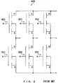
- Fig. 2 shows a semiconductor module 200 (so-called 6in1) such that six MOSFETs 201 are mounted on one insulation substrate.
- These semiconductor modules 100 and 200 configure the arm of an inverter apparatus for driving a motor.
- the semiconductor module 100 is configured in such a way that two MOSFETs 101 are connected in series.
- the semiconductor module 200 is configured in such a way that three circuits obtained by serially connecting MOSFETs 201 are connected in parallel.
- an IGBT (Insulated Gate Bipolar Transistor) semiconductor module obtained by connecting a plurality of IGBT semiconductor elements via an emitter terminal external connection part, a collector terminal external connection part and a gate terminal external connection part has been known.
- an inverted apparatus that uses this IGBT semiconductor module has been known. In this inverter apparatus, these two IGBT semiconductor modules are connected in series. In this series connection, wiring connection using bus bar wiring, etc. is used.
- This IGBT semiconductor module is obtained by connecting in parallel a plurality of, that is, at least two or more IGBT semiconductor elements in an inside thereof (for example, refer to a patent literature 1).
- Patent literature 1 Japanese Patent Laid-open Application Publication No. 10-84077
- the use application of a semiconductor module is increased by connecting in parallel and/or in series semiconductor elements in a semiconductor module.
- the semiconductor elements in the semiconductor module can be connected in parallel and/or in series, which is the main characteristic of the present invention.
- the present invention aims at offering a semiconductor apparatus according to the respective independent claim 1.
- the present invention can offer circuits in which modules are connected via various external connection terminals that implement the parallel connection and series connection of semiconductor elements, as one package of semiconductor apparatuses.
- the derating of an electric characteristic such as an allowable current capacity can be decreased by matching electric characteristics of semiconductor elements in the respective semiconductor modules.
- singe only an optional number of the semiconductor elements can be connected in parallel via an external connection terminal one package of products of many kinds can be offered as one package of semiconductor apparatuses. Accordingly, the production cost of those products can be reduced by the mass- production effect.
- semiconductor elements in a semiconductor module are configured to be externally connected via an external connection terminal (output to a motor) so that the semiconductor elements are externally connected to the 2in1. Therefore, the thus-connected module can be used as one MOS module.
- the semiconductor modules each having at least one semiconductor element are connected in parallel and/or in series via an external connection terminal to be offered as one package of products. Therefore, a variety of products can be provided as a package of semiconductor apparatuses.
- the component (the semiconductor module) canbe standardized in each product so that the production cost of each product can be reduced by the mass-production effect.
- the deratingof the electric characteristic of an allowable current, etc. can be reduced in comparison with the conventional product such that individual semiconductor packaged products are connected in parallel.
- a package of downsized products with different maximum allowable currents can be wisely produced so that an abundant product lineup can be offered to a user.
- Fig. 3 shows an example before a semiconductor apparatus of the preferred embodiment of the present invention is externally connected.
- the semiconductor apparatus shown in Fig. 3 is called a semiconductor apparatus substrate 10 for convenience.
- a case is provided with a MOS module part 12 (first MOS module part) and a MOS module part 14 (second MOS module part).
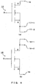
- Figs. 4 (a) and (b) are the circuit diagrams of the MOS module part 12 and the MOS module part 14, respectively. As shown in Figs. 4 (a) and (b) , each of the MOS module parts 12 and 14 is provided with enhancement-shaped MOSFETs (hereinafter, refer to n-MOSFET) 13 (first semiconductor module) and 15 (second semiconductor module) of an n channel in the case.
- enhancement-shaped MOSFETs hereinafter, refer to n-MOSFET 13 (first semiconductor module) and 15 (second semiconductor module) of an n channel in the case.
- the MOS module part 12 is provided with a terminal conductor 16 to be connected to a drain electrode (D) regarding the n-MOSFET 13 and terminal conductors 17-1 and 17-2 to be connected to a source electrode (S) .
- the MOS module part 14 is provided with terminal conductors 18-1 and 18-2 to be connected to a drain electrode (D) regarding the n-MOSFET 15 and a terminal conductor 19 to be connected to a source electrode (S).
- the terminal conductors 16, 17-1, 17-2, 18-1, 18-2 and 19 extend to the outside of the case and they are orthogonally bent at the outside of the case.
- Each of the MOS module parts 12 and 14 is provided with a gate electrode (G) which is not shown in Fig. 3 but shown in Figs. 4(a) and (b) .
- the semiconductor apparatus substrate 10 that is shown in Fig. 3 is only an example. In the present invention, therefore, the arrangement and the number of terminal conductors that are connected to the drain electrode on a semiconductor apparatus substrate and the terminal conductors that are connected to a source electrode are not limited.
- each electrode and terminal conductors can be configured to be integrated.
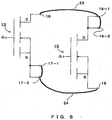
- Fig. 5 shows the method of producing a semiconductor apparatus in which the n-MOSFETs 13 and 15 of each of the MOS module part 12 and the MOS module part 14 are connected in parallel by externally connecting the MOS module 12 and the MOS module 14 of the semiconductor substrate 10 of Fig. 3 via external connection terminals 22, 24.
- the terminal conductor 16 that is connected to a drain electrode of the MOS module part 12 is externally connected to the terminal conductors 18-1 and 18-2 that are connected to the first and second drain electrodes of the MOS module part 14 via a positive electrode external connection terminal 22.
- the terminal conductors 17-1 and 17-2 that are connected to the first and second source electrodes of the MOS module part 12 and the terminal conductor 19 that is connected to the source electrode of the MOS module part 14 are connected via a negative electrode external connection terminal 24.
- Fig. 6 shows the circuit of a semiconductor apparatus 20 produced by externally connecting module parts via such external connection terminals 22 and 24.
- the semiconductor apparatus 20 is a circuit in which n-MOSFETs 13 and 15 are connected in parallel via external connection terminals 22, 24.
- the semiconductor apparatus 20 with the current capacity rating twice that of the n-MOSFETs 13 and 15 of each of the MOS module parts 12 and 14 can be produced by externally connecting the MOS module parts 12 and 14.
- the derating that is usually required can be reduced by making the electric characteristics of the n-MOSFETs 13 and 15 in each of the MOS module parts 12 and 14 approximately the same.
- FIG. 7 shows another semiconductor apparatus produced from the semiconductor apparatus substrate 10 of Fig. 3 .
- a semiconductor apparatus 30 that is shown in Fig.7 is the same as the semiconductor apparatus 20 of the example 1 in circuit and external connection configurations.
- an external connection terminal 32 includes a rectangle electric conductor flat plate that covers the conductor terminals 16, 17-1, 17-2, 18-1, 18-2 and 19 while an external connection terminal 34 includes a hexagon electric conductor flat plate that covers conductor terminals 17-1, 17-2 and 19.
- Fig. 8 is the partial cross-section view of a periphery part of the terminal conductor 17-2 along the line A-A' of the semiconductor apparatus 30 that is shown in Fig. 7 .
- the negative electrode external connection terminal 34 is provided on the surfaces of the MOS module parts 12 and 14 (not drawn in Fig. 8 ) like the shape shown in the top view of Fig. 7 and a sheet-shaped insulation part 36 is further provided so as to cover whole the negative electrode external connection terminal 34.
- a positive electrode external connection terminal 32 is provided on the insulation part 36.
- the positive electrode external connection terminal 32 is provided in the shape as shown on the top view of Fig. 7 . Therefore, a part of the positive electrode external connection terminal 32 is provided on the surfaces of the MOS module parts 12 and 14.
- the insulation part 36 is provided in order that the positive electrode external connection terminal 32 and the negative electrode external connection terminal 34 do not contact to each other.
- Each of the semiconductor apparatuses 20 and 30 of the above-mentioned example and preferred embodiment has the circuit configuration such that two semiconductor elements are connected in parallel.
- the circuit configuration of the semiconductor apparatus of the present invention is not limited to this configuration and the number of the semiconductor elements that are connected in parallel can be optional.
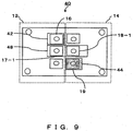
- Fig. 9 shows still another semiconductor apparatus produced from the semiconductor apparatus substrate 10 of Fig. 3 .
- a semiconductor apparatus 40 is configured in such a way that the MOS module parts 12 and 14 are externally connected via an intermediate external connection terminal 48 in addition to the positive electrode external connection terminal 42 and the negative electrode external connection terminal 44.
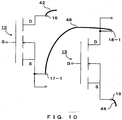
- Fig. 10 is the circuit diagram of the semiconductor apparatus 40.
- the terminal conductor 17-1 that is connected to the first source electrode of the n-MOSFET 13 of the MOS module part 12 is externally connected to the terminal conductor 18-2 that is connected to the second drain electrode of the n-MOSFET15 of the MOS module part 14, via the intermediate external connection terminal 48.
- the positive electrode external connection terminal 42 for the terminal conductor 16 that ifs connected to the drain electrode of the n-MOSFET 13 of the MOS module part 12 and the negative electrode external connection terminals 44 for the terminal conductor 19 that is connected to the source electrode of the n-MOSFET 15 of the MOS module part 14 are used for, for example, the series connection between module parts.
- the n-MOSFET 13 of the MOS module part 12 and the n-MOSFET15 of the MOS module part 14 are serially connected. Then, a semiconductor apparatus 40 of an arm configuration is produced by externally connecting modules via an external terminal. In this semiconductor apparatus 40, two n-MOSFETs 13 and 15 are serially connected. In the present example, however, the number of n-MOSFETs that are serially connected is not limited and the number is optional.
- n-MOSFETs are connected in parallel like the semiconductor apparatuses 20 and 30 of the example 1 and the preferred embodiment but also a circuit in which n-MOSFETs are connected in series like the semiconductor apparatus 40 of the example 2 can be configured.
- the semiconductor apparatus 20 or the semiconductor apparatus 30 and the semiconductor apparatus 40 are produced as one package of semiconductor apparatuses. Therefore, in the present invention, it is possible to produce as one package of semiconductor apparatuses a circuit in which n-MOSFETs are connected in parallel and in series.
- the semiconductor apparatus of each example and preferred embodiment uses the semiconductor module that is provided with an n-MOSFET as a semiconductor element.
- the semiconductor module that is used in the present invention can be provided with a semiconductor element other than an n-MOSFET.
- the semiconductor element of the present invention may include, for example, an FET, an IGBT, an SIT (Static Induction Transistor) such as a p-MOSFET, a CMOS-FET (Complementary Metal Oxide Semiconductor FET), etc., a transistor such as a bipolar transistor and a thyristor etc., such as a GTO (Gate Turn-off Thyristor).
- the number of the semiconductor elements that are mounted on the semiconductor module is not limited to one and an optional number can be adopted. Furthermore, the numbers of the respective semiconductor elements that are mounted on all the semiconductor modules need not be the same so that the numbers of semiconductor elements mounted on the respective semiconductor modules can be different. In addition, the types of the semiconductor elements that are mounted on the respective semiconductor modules can be different.
- the present invention can be applies to a device that is used for the control circuit and the power conversion apparatus etc. of a motor.
- the semiconductor apparatus (20) in which the n-MOSFET(13) of the MOS module part(12) and the n-MOSFET(15) of the MOS module part (14) are connected in parallel, is produced.
- the two n-MOSFETs are connected in series by externally connecting the source electrode of an n-MOSFET of the MOS module part(12) and a terminal conductor to be connected to a second drain electrode of the MOS module pat(14), via an intermediate external connection terminal.
Landscapes
- Semiconductor Integrated Circuits (AREA)
- Inverter Devices (AREA)
- Testing Of Individual Semiconductor Devices (AREA)
- Wire Bonding (AREA)
Claims (1)
- Halbleitervorrichtung (30), wobeieine Vielzahl von Halbleitermodulen (12, 14), die jeweils eine oder mehrere Halbleiterelemente, die jeweils erste und zweite Elektroden haben, aufweisen, in einem Gehäuse gespeichert sind,die Halbleitermodule jeweils einen ersten Anschlussleiter zum Herausführen einer ersten Elektrode von jedem Halbleiterelement zu einem Äußeren des Gehäuses und einen zweiten Anschlussleiter zum Herausführen einer zweiten Elektrode von jedem Halbleiterelement zu dem Äußeren des Gehäuses enthalten,ein erstes Halbleitermodul (12), das einen ersten Anschlussleiter (16) und zwei zweite Anschlussleiter (17-1, 17-2) enthält, und ein zweites Halbleitermodul (14), das zwei erste Anschlussleiter (18-1, 18-2) und einen zweiten Anschlussleiter (19) enthält, einander zugewandt sind,der eine erste Anschlussleiter (16) des ersten Halbleitermoduls (12) den zwei ersten Anschlussleitern (18-1, 18-2) des zweiten Halbleitermoduls (14) benachbart ist, und die zwei zweiten Anschlussleiter (17-1, 17-2) des ersten Halbleitermoduls (12) dem einen zweiten Anschlussleiter (19) des zweiten Halbleitermoduls (14) benachbart sind,die Vielzahl der Module innerhalb des Gehäuses parallel zueinander durch einen ersten externen Verbindungsanschluss (34), der die ersten Anschlussleiter der Halbleitermodule miteinander außerhalb des Gehäuses verbindet, und einen zweiten externen Verbindungsanschluss (32), der die zweiten Anschlussleiter der Halbleitermodule miteinander außerhalb des Gehäuses verbindet, verbunden sind,der erste externe Verbindungsanschluss (34), der den einen ersten Anschlussleiter (16) des ersten Halbleitermoduls (12) und die zwei ersten Anschlussleiter (18-1, 18-2) des zweiten Halbleitermoduls (14) bedeckt, eine elektrisch leitende flache Platte in einer konkaven hexagonalen Form ist,der zweite externe Verbindungsanschluss (32), der die ersten und zweiten Anschlussleiter (17-1, 17-2) des ersten Halbleitermoduls (12) und die ersten und zweiten Anschlussleiter (18-1, 18-2) des zweiten Halbleitermoduls (14) bedeckt, eine elektrisch leitende flache Platte in einer rechteckigen Form ist, undein Isolationsteil (36), das so geformt ist, dass es den ersten externen Verbindungsanschluss (34) bedeckt, zwischen den ersten und zweiten externen Verbindungsanschlüssen (32, 34) bereitgestellt ist.
Applications Claiming Priority (2)
| Application Number | Priority Date | Filing Date | Title |
|---|---|---|---|
| JP2004003174 | 2004-01-08 | ||
| JP2004003174A JP4363190B2 (ja) | 2004-01-08 | 2004-01-08 | 半導体装置及びその製造方法 |
Publications (3)
| Publication Number | Publication Date |
|---|---|
| EP1553687A2 EP1553687A2 (de) | 2005-07-13 |
| EP1553687A3 EP1553687A3 (de) | 2012-02-22 |
| EP1553687B1 true EP1553687B1 (de) | 2016-07-27 |
Family
ID=34587709
Family Applications (1)
| Application Number | Title | Priority Date | Filing Date |
|---|---|---|---|
| EP05000122.1A Expired - Lifetime EP1553687B1 (de) | 2004-01-08 | 2005-01-05 | Halbleitervorrichtung und Herstellungsverfahren für dieselbe |
Country Status (6)
| Country | Link |
|---|---|
| US (1) | US7397116B2 (de) |
| EP (1) | EP1553687B1 (de) |
| JP (1) | JP4363190B2 (de) |
| KR (1) | KR100679910B1 (de) |
| CN (1) | CN100521198C (de) |
| TW (1) | TWI256127B (de) |
Cited By (1)
| Publication number | Priority date | Publication date | Assignee | Title |
|---|---|---|---|---|
| US20250240010A1 (en) * | 2022-01-20 | 2025-07-24 | Mitsubishi Electric Corporation | Semiconductor device |
Families Citing this family (7)
| Publication number | Priority date | Publication date | Assignee | Title |
|---|---|---|---|---|
| JP4567570B2 (ja) * | 2005-10-17 | 2010-10-20 | 三菱電機株式会社 | 電力変換装置 |
| JP5055972B2 (ja) | 2006-01-12 | 2012-10-24 | 株式会社豊田自動織機 | 産業車両の荷役装置 |
| JP5333814B2 (ja) | 2007-09-12 | 2013-11-06 | アイシン精機株式会社 | パワー半導体モジュール、インバータ装置、及びインバータ一体型モータ |
| KR101410553B1 (ko) | 2010-07-01 | 2014-06-20 | 미쓰비시덴키 가부시키가이샤 | 파워 반도체 모듈, 전력 변환 장치, 및 철도 차량 |
| JP2012165621A (ja) * | 2011-02-09 | 2012-08-30 | Toshiba Corp | 電力変換装置 |
| CN103066862B (zh) * | 2012-12-26 | 2015-09-23 | 株洲南车时代电气股份有限公司 | 一种高压半桥igbt逆变模块 |
| DE102013102707A1 (de) * | 2013-03-18 | 2014-09-18 | Sma Solar Technology Ag | Wechselrichter mit mindestens einer Wechselrichterbrücke zwischen zwei Busbars |
Family Cites Families (13)
| Publication number | Priority date | Publication date | Assignee | Title |
|---|---|---|---|---|
| JPH0628292B2 (ja) | 1988-11-11 | 1994-04-13 | 富士電機株式会社 | 逆阻止形トランジスタモジュール |
| JP2656416B2 (ja) * | 1991-12-16 | 1997-09-24 | 三菱電機株式会社 | 半導体装置および半導体装置の製造方法、並びに半導体装置に用いられる複合基板および複合基板の製造方法 |
| JP2993278B2 (ja) * | 1992-06-26 | 1999-12-20 | 富士電機株式会社 | 半導体装置 |
| DE59509057D1 (de) * | 1994-11-07 | 2001-04-05 | Eupec Gmbh & Co Kg | Brücken-Modul |
| US5541453A (en) * | 1995-04-14 | 1996-07-30 | Abb Semiconductors, Ltd. | Power semiconductor module |
| CN1155165A (zh) | 1995-11-24 | 1997-07-23 | 亚瑞亚·勃朗勃威力有限公司 | 功率半导体组件系统 |
| JP3085453B2 (ja) | 1996-09-06 | 2000-09-11 | 株式会社日立製作所 | 半導体モジュール及びこれを用いたインバータ装置 |
| JP2000350475A (ja) | 1999-05-31 | 2000-12-15 | Hitachi Ltd | 半導体回路 |
| JP2001036005A (ja) | 1999-07-23 | 2001-02-09 | Fuji Electric Co Ltd | 半導体装置 |
| JP4177571B2 (ja) | 2001-09-20 | 2008-11-05 | 三菱電機株式会社 | 半導体装置 |
| JP4066644B2 (ja) * | 2001-11-26 | 2008-03-26 | 株式会社豊田自動織機 | 半導体装置、半導体装置の配線方法 |
| JP3780230B2 (ja) * | 2002-07-03 | 2006-05-31 | 株式会社日立製作所 | 半導体モジュール及び電力変換装置 |
| GB0226714D0 (en) * | 2002-11-15 | 2002-12-24 | Bombardier Transp Gmbh | Converter module |
-
2004
- 2004-01-08 JP JP2004003174A patent/JP4363190B2/ja not_active Expired - Fee Related
-
2005
- 2005-01-03 TW TW094100008A patent/TWI256127B/zh not_active IP Right Cessation
- 2005-01-04 US US11/029,915 patent/US7397116B2/en not_active Expired - Fee Related
- 2005-01-05 EP EP05000122.1A patent/EP1553687B1/de not_active Expired - Lifetime
- 2005-01-07 KR KR1020050001890A patent/KR100679910B1/ko not_active Expired - Fee Related
- 2005-01-10 CN CNB2005100038052A patent/CN100521198C/zh not_active Expired - Fee Related
Cited By (1)
| Publication number | Priority date | Publication date | Assignee | Title |
|---|---|---|---|---|
| US20250240010A1 (en) * | 2022-01-20 | 2025-07-24 | Mitsubishi Electric Corporation | Semiconductor device |
Also Published As
| Publication number | Publication date |
|---|---|
| KR20050074292A (ko) | 2005-07-18 |
| JP4363190B2 (ja) | 2009-11-11 |
| US7397116B2 (en) | 2008-07-08 |
| CN1638123A (zh) | 2005-07-13 |
| EP1553687A2 (de) | 2005-07-13 |
| TW200529409A (en) | 2005-09-01 |
| TWI256127B (en) | 2006-06-01 |
| JP2005198443A (ja) | 2005-07-21 |
| US20050151167A1 (en) | 2005-07-14 |
| EP1553687A3 (de) | 2012-02-22 |
| CN100521198C (zh) | 2009-07-29 |
| KR100679910B1 (ko) | 2007-02-07 |
Similar Documents
| Publication | Publication Date | Title |
|---|---|---|
| EP3246945B1 (de) | Leistungsmodul mit niedriger parasitärer induktivität | |
| EP3573096B1 (de) | Halbleitermodul | |
| US12003186B2 (en) | Power module for an electric drive of an electric vehicle or a hybrid vehicle, inverter comprising such a power module | |
| JPH0974198A (ja) | 高耐圧icおよびそれに用いる高耐圧レベルシフト回路 | |
| US6867494B2 (en) | Semiconductor module | |
| JP4164409B2 (ja) | 半導体パワーモジュール | |
| CN110168899B (zh) | 功率转换装置 | |
| EP1553687B1 (de) | Halbleitervorrichtung und Herstellungsverfahren für dieselbe | |
| JP6345361B2 (ja) | パワー半導体モジュール | |
| JPH0671063B2 (ja) | 大電力半導体装置 | |
| CN218633720U (zh) | 三相逆变器功率模块和三相逆变器功率设备 | |
| US8023276B2 (en) | Circuit arrangement comprising having plurality of half bridges | |
| US20170033705A1 (en) | Semiconductor device | |
| JP2003502834A (ja) | 半導体素子 | |
| JP2002171768A (ja) | 電力変換装置 | |
| US6838830B2 (en) | Half-bridge | |
| US12451878B2 (en) | High-voltage bidirectional field effect transistor | |
| US11679680B2 (en) | Power module for operating an electric vehicle drive with an intermediate circuit capacitor | |
| US20230307332A1 (en) | Power Semiconductor Module and Method for Producing a Power Semiconductor Module | |
| JPH10225138A (ja) | 電力変換回路及びインバータ装置 | |
| US20260088729A1 (en) | Current converter, electric drive device and method for manufacturing a current converter | |
| CN120418963A (zh) | 功率半导体装置 | |
| KR20010060778A (ko) | 전력 반도체 모듈의 수분침투 방지장치 | |
| JP2026013098A (ja) | 電力半導体装置 | |
| JPH11312771A (ja) | 半導体装置及び半導体装置の配置方法 |
Legal Events
| Date | Code | Title | Description |
|---|---|---|---|
| PUAI | Public reference made under article 153(3) epc to a published international application that has entered the european phase |
Free format text: ORIGINAL CODE: 0009012 |
|
| 17P | Request for examination filed |
Effective date: 20050105 |
|
| AK | Designated contracting states |
Kind code of ref document: A2 Designated state(s): AT BE BG CH CY CZ DE DK EE ES FI FR GB GR HU IE IS IT LI LT LU MC NL PL PT RO SE SI SK TR |
|
| AX | Request for extension of the european patent |
Extension state: AL BA HR LV MK YU |
|
| PUAL | Search report despatched |
Free format text: ORIGINAL CODE: 0009013 |
|
| AK | Designated contracting states |
Kind code of ref document: A3 Designated state(s): AT BE BG CH CY CZ DE DK EE ES FI FR GB GR HU IE IS IT LI LT LU MC NL PL PT RO SE SI SK TR |
|
| AX | Request for extension of the european patent |
Extension state: AL BA HR LV MK YU |
|
| RIC1 | Information provided on ipc code assigned before grant |
Ipc: H01L 27/02 20060101ALI20120119BHEP Ipc: H02M 7/00 20060101AFI20120119BHEP |
|
| AKX | Designation fees paid |
Designated state(s): DE FR GB IT SE |
|
| 17Q | First examination report despatched |
Effective date: 20150817 |
|
| GRAP | Despatch of communication of intention to grant a patent |
Free format text: ORIGINAL CODE: EPIDOSNIGR1 |
|
| INTG | Intention to grant announced |
Effective date: 20160406 |
|
| RIN1 | Information on inventor provided before grant (corrected) |
Inventor name: ONISHI, HIROYUKI Inventor name: AKAGAWA, KOICHI Inventor name: ISHIKAWA, JUN Inventor name: NAGASE, TOSHIAKI |
|
| GRAS | Grant fee paid |
Free format text: ORIGINAL CODE: EPIDOSNIGR3 |
|
| GRAA | (expected) grant |
Free format text: ORIGINAL CODE: 0009210 |
|
| AK | Designated contracting states |
Kind code of ref document: B1 Designated state(s): DE FR GB IT SE |
|
| REG | Reference to a national code |
Ref country code: GB Ref legal event code: FG4D |
|
| REG | Reference to a national code |
Ref country code: DE Ref legal event code: R096 Ref document number: 602005049805 Country of ref document: DE |
|
| REG | Reference to a national code |
Ref country code: SE Ref legal event code: TRGR |
|
| REG | Reference to a national code |
Ref country code: FR Ref legal event code: PLFP Year of fee payment: 13 |
|
| REG | Reference to a national code |
Ref country code: DE Ref legal event code: R097 Ref document number: 602005049805 Country of ref document: DE |
|
| PLBE | No opposition filed within time limit |
Free format text: ORIGINAL CODE: 0009261 |
|
| STAA | Information on the status of an ep patent application or granted ep patent |
Free format text: STATUS: NO OPPOSITION FILED WITHIN TIME LIMIT |
|
| 26N | No opposition filed |
Effective date: 20170502 |
|
| REG | Reference to a national code |
Ref country code: FR Ref legal event code: PLFP Year of fee payment: 14 |
|
| PGFP | Annual fee paid to national office [announced via postgrant information from national office to epo] |
Ref country code: FR Payment date: 20181213 Year of fee payment: 15 |
|
| PGFP | Annual fee paid to national office [announced via postgrant information from national office to epo] |
Ref country code: GB Payment date: 20190102 Year of fee payment: 15 Ref country code: DE Payment date: 20181228 Year of fee payment: 15 Ref country code: IT Payment date: 20190121 Year of fee payment: 15 |
|
| PGFP | Annual fee paid to national office [announced via postgrant information from national office to epo] |
Ref country code: SE Payment date: 20190110 Year of fee payment: 15 |
|
| REG | Reference to a national code |
Ref country code: DE Ref legal event code: R119 Ref document number: 602005049805 Country of ref document: DE |
|
| REG | Reference to a national code |
Ref country code: SE Ref legal event code: EUG |
|
| GBPC | Gb: european patent ceased through non-payment of renewal fee |
Effective date: 20200105 |
|
| REG | Reference to a national code |
Ref country code: SE Ref legal event code: EUG |
|
| PG25 | Lapsed in a contracting state [announced via postgrant information from national office to epo] |
Ref country code: FR Free format text: LAPSE BECAUSE OF NON-PAYMENT OF DUE FEES Effective date: 20200131 Ref country code: GB Free format text: LAPSE BECAUSE OF NON-PAYMENT OF DUE FEES Effective date: 20200105 Ref country code: DE Free format text: LAPSE BECAUSE OF NON-PAYMENT OF DUE FEES Effective date: 20200801 Ref country code: SE Free format text: LAPSE BECAUSE OF NON-PAYMENT OF DUE FEES Effective date: 20200106 |
|
| PG25 | Lapsed in a contracting state [announced via postgrant information from national office to epo] |
Ref country code: IT Free format text: LAPSE BECAUSE OF NON-PAYMENT OF DUE FEES Effective date: 20200105 |