EP1553761B1 - Dispositif recepteur et recepteur de television - Google Patents
Dispositif recepteur et recepteur de television Download PDFInfo
- Publication number
- EP1553761B1 EP1553761B1 EP03771350A EP03771350A EP1553761B1 EP 1553761 B1 EP1553761 B1 EP 1553761B1 EP 03771350 A EP03771350 A EP 03771350A EP 03771350 A EP03771350 A EP 03771350A EP 1553761 B1 EP1553761 B1 EP 1553761B1
- Authority
- EP
- European Patent Office
- Prior art keywords
- filter
- shield
- high frequency
- receiving device
- frame
- Prior art date
- Legal status (The legal status is an assumption and is not a legal conclusion. Google has not performed a legal analysis and makes no representation as to the accuracy of the status listed.)
- Expired - Lifetime
Links
Images







Classifications
-
- H—ELECTRICITY
- H05—ELECTRIC TECHNIQUES NOT OTHERWISE PROVIDED FOR
- H05K—PRINTED CIRCUITS; CASINGS OR CONSTRUCTIONAL DETAILS OF ELECTRIC APPARATUS; MANUFACTURE OF ASSEMBLAGES OF ELECTRICAL COMPONENTS
- H05K9/00—Screening of apparatus or components against electric or magnetic fields
- H05K9/0007—Casings
- H05K9/006—Casings specially adapted for signal processing applications, e.g. CATV, tuner, antennas amplifier
-
- H—ELECTRICITY
- H04—ELECTRIC COMMUNICATION TECHNIQUE
- H04N—PICTORIAL COMMUNICATION, e.g. TELEVISION
- H04N21/00—Selective content distribution, e.g. interactive television or video on demand [VOD]
- H04N21/40—Client devices specifically adapted for the reception of or interaction with content, e.g. set-top-box [STB]; Operations thereof
- H04N21/41—Structure of client; Structure of client peripherals
- H04N21/426—Internal components of the client ; Characteristics thereof
-
- H—ELECTRICITY
- H04—ELECTRIC COMMUNICATION TECHNIQUE
- H04N—PICTORIAL COMMUNICATION, e.g. TELEVISION
- H04N5/00—Details of television systems
- H04N5/44—Receiver circuitry for the reception of television signals according to analogue transmission standards
-
- H—ELECTRICITY
- H04—ELECTRIC COMMUNICATION TECHNIQUE
- H04N—PICTORIAL COMMUNICATION, e.g. TELEVISION
- H04N5/00—Details of television systems
- H04N5/64—Constructional details of receivers, e.g. cabinets or dust covers
-
- H—ELECTRICITY
- H04—ELECTRIC COMMUNICATION TECHNIQUE
- H04N—PICTORIAL COMMUNICATION, e.g. TELEVISION
- H04N5/00—Details of television systems
- H04N5/44—Receiver circuitry for the reception of television signals according to analogue transmission standards
- H04N5/50—Tuning indicators; Automatic tuning control
Definitions
- the present invention relates to a receiving device for receiving a high frequency input signal through a receiving antenna and the television receiver including the receiving device.
- the television receiver includes a receiving device that receives a high frequency input signal through an antenna.
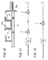
- a so-called heterodyne system is employed as shown in FIG. 11 .
- a high frequency input signal f is input to an antenna 1000.
- the high frequency input signal f is mixed with a mixing frequency f1 to be selected, so that the intermediate frequency (f-f1) is obtained.
- the intermediate frequency (f-f1) is mixed with a constant frequency f2, and a base band signal ((f-f1)-f2) is obtained.
- This base band frequency has a range of DC (direct current) to several ten MHz.
- a direct conversion system having a small number of components and a simple structure is beginning to be used.
- the direct conversion system when a high frequency input signal f is input to an antenna 1010, the mixing frequency f1 which is the same as the selection frequency is mixed with the high frequency input signal, and the differential signal is taken out to obtain (f-f1) as a base band signal.
- an amplifier 1020, a filter 1024, a direct conversion unit 1026 and a digital demodulator 1028 are formed on a substrate 1016.
- a shield case 1030 and a shield cover 1040 are detachably loaded onto the substrate 1016, and the shield case 1030 and shield cover 1040 shield each elements on the substrate 1016 from high frequency waves.
- the shield cover 1040 is engaged with ribs 1061 in the shield case 1030, using a plurality of claws 1060 on the peripheral portion thereof to be hooked, and the shield cover 1040 and shield case 1030 are contacted and fixed to each other.
- the shield case 1030 has a frame 1055, and an inner partition plate 1056 is disposed in the center of the frame 1055.
- the frame 1055 has a plurality of claws 1050, and when the claws 1050 are fixed into concave portions 1017 in the substrate 1016, the shield case 1030 is fixed to the substrate 1016.
- the amplifier 1020, the filter 1024, the direct conversion unit 1026 and the digital demodulator 1028, each of which is a functional block of the substrate 1016, are surrounded and shielded.
- the inner partition plate 1056 of the shield case 1030 is, for example, disposed to shield between the filter 1024 and the direct conversion unit 1026, where the partition plate 1056 is soldered to the ground of the substrate 1016 to function as a shield plate.
- the ground impedance is lowest at the portion soldered with the ground of the substrate 1016; however, the ground impedance of a portion of the shield case which is far from the inner partition plate 1056 becomes high.
- a plurality of claws 1060 and a spring-shaped weight 1070 in the shield cover 1040 are only in contact with the shield case 1030 side, and the other portions of the shield cover and shield case are not contacted; thus, no other portion than the plurality of claws 1060 and the spring-shaped weight 1070 is provided where the ground impedance becomes low.
- High frequency electric current is easily induced at the portion where the ground impedance is high, and with the induced current the high frequency energy may again radiate into the space, so that efficient shielding can not sufficiently be obtained when a conventional shield cover and shield case are used.
- the high frequency input signal f which is the receiving signal
- the high frequency energy becomes highly strong at the initial stage amplifier 1020 and also at the filter 1024 of a sub-tuning band-pass filter and others.
- high frequency energy is easily radiated from the filter 1024 due to the Q value of a circuit in the substrate 1016. The problem (of so-called pulling) that this radiated energy affects the local frequency of selection unit occurs in a receiving device employing the direct conversion system.
- JP 2000 294950 describes a high frequency apparatus with metallic shield cases.
- JP 11 163755A describes an up/down tuner in which an up-converter and a down-converter are contained in separate respective chassis.
- the present invention aims to provide a receiving device and a television receiver, in which the above problem is solved and the shielding performance is improved to solve the pulling problem in the receiving device employing the direct conversion system.
- the present invention provides a receiving device (10) comprising:
- a shield case made to stand on the boundary between the filter and the other units can surround the filter.
- a shield cover is disposed to cover the shield case and prevents the leakage of radiation of high frequency electro-magnetic waves generated from the filter into the space, so that the pulling problem in a receiving device having the direct conversion system can be solved.
- the above shield cover has: a main surface, a part of which is deeply bent to form a dropped-lid shape and which covers the filter, and a first surface-contact portion and a second surface-contact portion formed to oppose to each other on both end portions of the main surface, which stand up from the main surface portion with a predetermined height and are disposed to come in surface contact with the shield plate portion of the shield case; in which the first surface-contact portion is provided at the boundary between the main surface portion and a portion that is not deeply bent of the shield cover.
- the shield cover is in surface contact with the shield plate portion of the shield case with the first and second surface-contact portions, the effectiveness of shielding of the substrate can further be improved.
- the second surface-contact portion of the shield cover is formed to have an angle larger than a right angle with respect to the main surface portion.
- the shield cover when covering the shield case, the shield cover can be prevented from pulling off.
- the present invention is a television receiver having the above mentioned receiving device, further including: a digital demodulator that demodulates a transport stream from an output of a detector, a data separator that separates compressed data of the desired program from data multiplexed in the transport stream from the digital demodulator, an MPEG demodulator that expands a compressed data of the program from the data separator, an image processor that converts the expanded data from the MPEG demodulator into a video output signal, and a display that displays the video output signal from the image processor.
- a digital demodulator that demodulates a transport stream from an output of a detector
- a data separator that separates compressed data of the desired program from data multiplexed in the transport stream from the digital demodulator
- an MPEG demodulator that expands a compressed data of the program from the data separator
- an image processor that converts the expanded data from the MPEG demodulator into a video output signal
- a display that displays the video output signal from the image processor.
- the substrate has an amplifier that amplifies a high frequency input signal, a filter that passes only an intended signal and removes an unintended signal by tuning the amplified high frequency input, and a detector that performs direct conversion on the high frequency input signal from a filter to be detected.
- the shield case stands at the boundary between a filter and the other unit to surround the filter.
- a shield cover is disposed to cover the filter surrounded by the shield case. The shield cover prevents the leakage of radiation of high frequency electro-magnetic waves from the filter into the space.
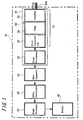
- FIG. 1 shows a television receiver as an example of electronic equipment having a receiving device according to the present invention.
- a television receiver 14 includes a receiving device 10, a data separator 42, an MPEG demodulator 44, an image processor 46 and a display 48.
- the receiving device 10 has a substrate 20 (also call a circuit board), and the substrate 20 has an amplifier 30, a filter 34, a direct conversion unit 36 and a digital demodulator 40.
- the amplifier 30, the filter 34, the direct conversion unit 36 and the digital demodulator 40 are the functional blocks formed on the substrate 20.
- the amplifier 30 is connected to a receiving antenna through a connector 90A, and the receiving antenna receives a high frequency input signal f.
- the high frequency input signal f is amplified in the amplifier 30.
- the filter 34 makes the amplified high frequency input signal tuned to pass only an intended signal and also to remove an unintended signal, and the filter 34 generates a tuning frequency (a local frequency) f1.
- the direct conversion unit 36 generates a base band (f-f1) by subtracting a local frequency f1 generated in the filter 34 from the high frequency input signal f. Specifically, the direct conversion unit 36 has a function of tuning the amplified high frequency input signal f to a local frequency f1 generated in the filter 34 to convert directly and detect.
- the digital demodulator 40 has a function of demodulating a transport stream from a modulated digital signal.
- a data separator 42 performs in a unit of packets filtering of video information, audio information, program specifying information, program arrangement information, data broadcast information, and others which are multiplexed with a digitally demodulated transport stream, to separate and select compressed data of the desired program.
- the MPEG demodulator 44 expands compressed data of the program separated by the data separator 42.
- the image processor 46 outputs a video output signal from the expanded data by the MPEG demodulator 44, and displays an image on the display 48 of a plasma display or the like, for example. Also, audio information is processed in an audio processor not shown in the drawing to be output from a speaker or the like.
- FIG. 2 shows an embodiment of the receiving device 10 of FIG. 1 .
- the receiving device 10 has a substrate 20, a shield cover 60 and a shield case 90.
- the shield cover 60 and the shield case 90 are made of, for example, metal such as aluminum that can prevent the leakage of a high frequency electro-magnetic wave.
- the shield cover 60 covers the shield case 90 and is detachably attached thereto.
- the shield case 90 is attached detachably to the substrate 20.
- FIG. 3 shows the state in which only the shield case 90 is installed on the substrate 20, and the shield cover 60 is removed from the shield case 90.
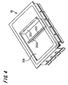
- FIG. 4 shows the structure of the shield cover 60.
- FIG. 5A shows an example of the shape of cross section on A-A line of FIG. 2 .
- the amplifier 30, the filter 34, the direct conversion unit 36 and the digital demodulator 40 are formed sequentially on the one side surface of the substrate 20.
- FIG. 5B shows the state in which projections 170 of the shield case 90 are inserted into holes 173 of the substrate 20, and soldered.
- FIG. 5C shows the other side surface of the substrate 20, in which the projections 170 of the shield case 90 are inserted into the holes 173 of the substrate 20, though not yet soldered.
- a ground pattern 171 is formed on almost whole the surface on the other side surface of a substrate 20; rounds 175 are provided around the holes 173 of the substrate 20; the rounds 175 and projections 170 of the shield case 90 are soldered to fix the shield case 90 and the shield case 90 is electrically connected to the ground pattern 171; and thus, the shield case 90 can be grounded.
- the shield case 90 By covering the shield case 90 with the shield cover 60, the leakage of radiation of high frequency generated from the filter into the space is efficiently prevented.
- the shield case 90 is formed by bending and punching out, for example, an aluminum plate, which corresponds to the first high-frequency shielding portion.
- the shield cover 60 corresponds to the second high-frequency shielding portion.
- the shield case 90 functioning as the first high-frequency shielding portion is formed to surround the above mentioned amplifier 30, filter 34 and direct conversion unit 36.
- the shield case 90 has a first frame 100 that surrounds the amplifier 30, a second frame 101 that surrounds the filter 30 and a third frame 102 that surrounds the direct conversion unit 36.
- the first frame 100, the second frame 101 and the third frame 102 are continuously formed.
- the first frame 100 is formed to stand at the boundary between the amplifier 30 and the other units and to surround the amplifier 30, having side surface portions 110, 111, 112 and 113.
- the second frame 101 is formed to stand at the boundary between the filter 34 and the other units and to surround the filter 34, having a first shield plate portion 115, a second shield plate portion 117, a third shield plate portion 118 and a fourth shield plate portion 119.
- the side surface portion 110 and the side surface portion 113 of the first frame 100 oppose to each other as shown in FIG. 3 , and also the side surface portion 111 and the side surface portion 112 oppose to each other. Those four side surface portions 110 to 113 are formed to stand to separate the amplifier 30 and the filter 34 that is the other unit.
- the first shield plate portion 115 and the second shield plate portion 117 of the second frame 101 oppose to each other, and also the third shield plate portion 118 and the fourth shield plate portion 119 oppose to each other.
- the first shield plate portion 115 is formed to stand at the first boundary between the amplifier 30 and the filter 34.
- the second shield plate portion 117 is formed to stand at the second boundary between the filter 34 and the direct conversion unit 36.
- the third shield plate portion 118 and the fourth shield plate portion 119 are formed to stand between the filter 34 and the outside. Accordingly, the second frame 101 is formed to stand at the boundaries of four corners of a rectangular-shaped filter 34 so that high frequency electro-magnetic waves can be shielded. Note that the side surface portion 113 and the first shield plate portion 115 are formed of the portion used in common.
- the third frame 102 has side surface portions 130, 131, 132 and 133 to surround the direct conversion unit 36.
- the side surface portions 130 and 132 oppose to each other, and the side surface portions 131 and 133 also oppose to each other.
- the side surface portion 130 is disposed at the boundary between the filter 34 and the direct conversion unit 36.
- the side surface portion 132 is disposed to stand at the boundary between the direct conversion unit 36 and the digital demodulator 40.
- the side surface portion 131 and a side surface portion 133 are provided to stand at the boundary between the direct conversion unit 36 and the outside. Further the side surface portion 130 and the second shield plate portion 117 are formed of the portion used in common.
- ribs 150 are formed with a projection in the directions parallel to the X and Y directions of the substrate 20.
- FIG. 3 shows a pair of ribs 150 and 150 at the front side, and also the same ribs 150 and 150 are formed on the two surfaces of the rear side.
- the shield case 90 has a plurality of projections 170 on the first shield plate portion 115 and the second shield plate portion 117. As shown in FIGS. 5B and 5C , those projections 170 are inserted into the holes 173 formed on the substrate 20 and are grounded by being soldered with the lands of the ground pattern provided close to the holes 173; and the shield case 90 is attached to the substrate 20 through the projections 170.
- the shield cover 60 is formed by bending metal such as aluminum or the like, for example, and is a member having an almost rectangular shape. As shown in FIG. 2 , the shield cover 60 covers a shield case 90 shown in FIG. 3 and is fixed detachably.
- the shield cover 60 is jointly used with the shield case 90 as the first high-frequency shielding portion to prevent the leakage of radiation in the space from the amplifier 30, the filter 34, the direct conversion unit 36 and the digital demodulator 40. Particularly, as shown in FIG. 5A , the main surface portion 200 of the shield cover 60 comes close to the surface and covers the filter 34. Accordingly, high frequency electro-magnetic waves generated in the filter 34 and radiated to the outside can be prevented completely.
- the shield cover 60 in FIG. 2 has a frame 201, the main surface portion 200, a first surface-contact portion 202, a second surface-contact portion 203, a hole 204 and the like.
- the frame 201 is formed of a rectangular shape, and as shown in FIG. 6 , a plurality of claws 220, 230, 240 and 250 are formed downward on those four side surfaces.
- FIG. 7A shows a cross section of C-C line in FIG. 6
- FIG. 7B shows a cross section of B-B line in FIG. 6 .
- the first surface-contact portion 202, the second surface-contact portion 203 and the main surface portion 200 are formed by bending a double-sided surface portion 206 of the frame 201 to have a dropped-lid shaped portion 210.
- the dropped-lid shape portion 210 is provided at the position facing the filter 34. Then, the first surface-contact portion 202 is bent at right angles with respect to the surface portion 206, the main surface portion 200 is further bent at right angles with respect to the first surface-contact portion 202, and furthermore the second surface-contact portion 202 is bent at right angles with respect to the main surface portion 200. Therefore, the dropped-lid shape portion 210 has almost a U-shape when seeing the cross section thereof.
- the inside surface of the first surface-contact portion 202 is in surface contact with the outside surface of the first shield plate portion 115 of the shield case 90.
- the inside surface of the second surface-contact portion 203 is in surface contact with the outside surface of the second shield plate portion 117 of the shield case 90.
- the main surface portion 200 faces the position of the filter 34 where a small gap is provided, namely, the main surface portion comes close to the filter.
- high frequency electromagnetic waves generated from the filter 34 can be prevented completely from radiating into the space to the outside, using the first shield plate portion 115, the second shield plate portion 117, the third shield plate portion 118 and the fourth shield plate portion 119 shown in FIG. 3 and the main surface portion 200, the first surface-contact portion 202 and the second surface-contact portion 203 shown in FIG. 5A .
- the end portion of the second surface-contact portion 203 becomes an L-shaped bent portion 203A and this bent portion 203A comes in contact with the upper end surface of the second shielding portion 117. Accordingly, the main surface portion 200 can be positioned and disposed in parallel with respect to the filter 34 in the state of facing close thereto.
- the shield case 90 has a connector to connect to an antenna 45.
- the hole 204 is formed facing the position of the direct conversion unit 36.
- the shield cover 60 has the above mentioned claws 220, 230, 240 and 250, and the shield cover 60 can be fixed detachably to cover the shield case 90 with engaging those claws with the ribs 150 of the shield case 90 in FIG. 2 that is formed at the corresponding position.
- a receiving device of the embodiment of the present invention uses a so-called direct conversion system, in which the filter 34 having a sub-tuning band pass filter and others may secondarily radiate larger high-frequency energy in comparison with the other units in the receiving device.
- the shield case 90 and shield cover 60 have the structure in which not only the filter 34 that radiates the highest high frequency energy secondarily, but also the amplifier 30 and the direct conversion unit 36 as shown in FIG. 5A can be shielded.
- the shield cover 60 and shield case 90 are provided with the dropped-lid shaped portion 210 as mentioned above with respect to the filter 34 which generates the highest high-frequency energy (high frequency electromagnetic waves); and the first surface-contact portion 202, the second surface-contact portion 203 and the main surface portion 200 of the dropped-lid shaped portion 210 of the shield cover 60 and the first shield plate portion 115, the second shield plate portion 117, the third shield plate portion 118 and the fourth shield plate portion 119 of the shield case 90 shown in FIG. 3 are combined to be used, so that the radiation of the high frequency energy to the outside space from the filter 34 can be prevented.
- the shield cover 60 and the shield case 90 are in surface contact using the first surface-contact portion 202 and the second surface-contact portion 203 of the dropped-lid shaped portion 210, and the first shield plate portion 115 and the second shield plate portion 117 of a shield case 90. Accordingly, the strong surface-contact portion between the shield cover 60 and the second shield plate portion 117 as the partition plate can be constructed close to the position where the second shield plate portion 117 having the lowest impedance with respect to high frequency and the ground of the substrate 20 are soldered. Therefore, a ground impedance of the shield cover 60 can be greatly reduced. Consequently, the induction of high frequency current can be reduced by obtaining the decrease in ground impedance; as a result, the re-radiation of high frequency electromagnetic waves can be reduced greatly.
- the shield cover 60 as the second high-frequency shielding portion has dimensions that can cover all the shield case 90.
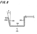
- the second surface-contact portion 203 of a dropped-lid shaped portion 210 is formed with tilt by ⁇ as shown in FIG. 8 in the released state.
- the dropped-lid shaped portion 210 is inserted by force into the portion between the first shield plate portion 115 and the second shield plate portion 117 of the shield case 90, so that the dropped-lid shaped portion 210 may not be detached from the shield case 90 using an elasticity of the second surface-contact portion 203.
- FIGS. 9 and 10 show another embodiment of the present invention.
- a shield cover 360 as the second high-frequency shielding portion is made smaller in comparison with the shield cover 60 shown in FIG. 2 .
- the shield cover 360 is attached to the ribs 150 of the shield case 90 using the claws 220.
- the shield cover 360 has the structure only facing the filter 34 as shown in FIG. 10 .
- the shield case 90 shown in FIGS. 9 and 10 can use the same structure of the shield case 90 shown in FIG. 2 .
- the substrate 20 is the same as that shown in FIG. 2 .
- the shield cover 360 has a frame 301 and a dropped-lid shaped portion 310.
- the dropped-lid shaped portion 310 has the first surface-contact portion 202, the second surface-contact portion 203 and the main surface portion 200. Therefore, the structure of the dropped-lid shaped portion 310 is almost the same as the dropped-lid shaped portion 210 shown in FIG. 2 .
- the first shield plate portion 115 is in surface contact with the first surface-contact portion 202.
- the second shield plate portion 117 is in surface contact with the second surface-contact portion 203.
- the main surface portion 200 faces the filter 34 having a small space in between.
- the shield cover 360 can be small-sized using such structure, and particularly the radiation from the filter 34 which secondarily induces high frequency electro-magnetic waves can be prevented.
- the shielding performance in a filter which particularly radiates high frequency electro-magnetic waves secondarily in a receiving device of a so-called direct conversion system can be improved, so that the pulling problem in a receiving device of the direct conversion system can be solved.
- a shield cover has a dropped-lid shaped portion
- the positions of a shield cover and a shield case can be easily determined mutually using the dropped-lid shaped portion, and consequently assembly can be performed easily to improve the assembling operation efficiency.
- a receiving device of a direct conversion system radiation of high frequency electromagnetic waves from a filter to the space can be reduced by disposing a dropped-lid shaped portion with respect to the filter in the case where an amplifier (amplifier circuit unit) and a subsequent filter (also called filter circuit unit) are covered by a shield cover.
- an amplifier amplifier circuit unit
- a subsequent filter also called filter circuit unit
- a receiving device is installed in a television receiver as an example of electronic equipment.
- a receiving device of the present invention is not limited thereto and can also be applied to the other types of electronic equipment.
Landscapes
- Engineering & Computer Science (AREA)
- Signal Processing (AREA)
- Multimedia (AREA)
- Microelectronics & Electronic Packaging (AREA)
- Shielding Devices Or Components To Electric Or Magnetic Fields (AREA)
- Structure Of Receivers (AREA)
- Noise Elimination (AREA)
Abstract
Claims (5)
- Dispositif de réception (10) comprenant :un substrat (20) pourvu d'un amplificateur (30) qui amplifie un signal d'entrée haute fréquence, d'un filtre (34) qui ne laisse passer qu'un signal souhaité après avoir accordé le signal d'entrée haute fréquence amplifié par ledit amplificateur (30), et d'une unité de conversion directe (36) dans laquelle le signal d'entrée haute fréquence provenant dudit filtre (34) est mélangé avec un signal local ayant la même fréquence que le signal d'entrée pour obtenir un signal de bande de base ;un boîtier de blindage (90) qui est constitué d'une tôle et qui entoure ledit amplificateur (30), ledit filtre (34) et ladite unité de conversion directe (36), le cadre de blindage comportant un cadre (101) qui entoure ledit filtre (34) et le sépare des autres unités et qui comporte une pluralité de protubérances (170) qui sont insérées dans un ensemble de trous (173) formés sur ledit substrat, lesdites protubérances (170) étant mises à la masse électriquement par leur soudage à un motif de masse (171) prévu autour desdits trous (173) ; etun capot de blindage métallique (60) qui recouvre au moins le cadre (101) entourant ledit filtre (34) et qui comporte une partie en forme de couvercle surbaissé (210) pour s'approcher dudit filtre (34).
- Dispositif de réception selon la revendication 1, dans lequel
un démodulateur numérique (40) qui démodule un flot de transport provenant d'une sortie de ladite unité de conversion directe est en outre prévu sur ledit substrat. - Dispositif de réception selon la revendication 1, dans lequel
ledit capot de blindage comporte une partie en forme de couvercle surbaissé (210) qui est pliée pour former la forme de couvercle surbaissé et un cadre qui est formé en pliant ladite partie en forme de couvercle surbaissé ; et
ladite partie en forme de couvercle surbaissé comporte une partie de surface principale (200) qui recouvre ledit filtre, une première partie de contact de surface (202) formée entre la partie de surface principale et ledit cadre pour être en contact de surface avec ledit cadre, et une deuxième partie de contact de surface (203) formée à l'opposé de la première partie de contact de surface pour être en contact de surface avec ledit cadre. - Dispositif de réception selon la revendication 3, dans lequel
ladite deuxième partie de contact de surface est formée selon un angle sans se séparer dudit boîtier de blindage, lorsqu'elle recouvre ledit boîtier de blindage. - Récepteur de télévision (14) comprenant un dispositif de réception selon la revendication 1, comprenant en outre :un démodulateur numérique (40) qui démodule un flot de transport provenant d'une sortie dudit détecteur ;un séparateur de données (42) qui sépare les données compressées du programme souhaité des données multiplexées dans le flot de transport provenant dudit démodulateur numérique ;un démodulateur MPEG (44) qui décompresse les données compressées du programme souhaité provenant dudit séparateur de données ;un processeur d'image (46) qui convertit les données décompressées provenant dudit démodulateur MPEG en un signal de sortie vidéo ; etun afficheur (48) qui affiche un signal de sortie vidéo provenant dudit processeur d'image.
Applications Claiming Priority (3)
| Application Number | Priority Date | Filing Date | Title |
|---|---|---|---|
| JP2002216687 | 2002-07-25 | ||
| JP2002216687 | 2002-07-25 | ||
| PCT/JP2003/009472 WO2004012446A1 (fr) | 2002-07-25 | 2003-07-25 | Dispositif recepteur et recepteur de television |
Publications (3)
| Publication Number | Publication Date |
|---|---|
| EP1553761A1 EP1553761A1 (fr) | 2005-07-13 |
| EP1553761A4 EP1553761A4 (fr) | 2007-08-29 |
| EP1553761B1 true EP1553761B1 (fr) | 2009-08-26 |
Family
ID=31184583
Family Applications (1)
| Application Number | Title | Priority Date | Filing Date |
|---|---|---|---|
| EP03771350A Expired - Lifetime EP1553761B1 (fr) | 2002-07-25 | 2003-07-25 | Dispositif recepteur et recepteur de television |
Country Status (7)
| Country | Link |
|---|---|
| US (1) | US7224953B2 (fr) |
| EP (1) | EP1553761B1 (fr) |
| JP (1) | JP4341554B2 (fr) |
| KR (1) | KR101015689B1 (fr) |
| CN (1) | CN100493155C (fr) |
| DE (1) | DE60329010D1 (fr) |
| WO (1) | WO2004012446A1 (fr) |
Cited By (1)
| Publication number | Priority date | Publication date | Assignee | Title |
|---|---|---|---|---|
| US9980418B2 (en) | 2014-02-18 | 2018-05-22 | Thomson Licensing | RF shield assembly |
Families Citing this family (19)
| Publication number | Priority date | Publication date | Assignee | Title |
|---|---|---|---|---|
| JP3100213U (ja) * | 2003-09-03 | 2004-05-13 | アルプス電気株式会社 | テレビジョンチューナ |
| JP3100214U (ja) * | 2003-09-03 | 2004-05-13 | アルプス電気株式会社 | テレビジョンチューナ |
| JP4182430B2 (ja) * | 2003-11-28 | 2008-11-19 | オムロン株式会社 | 送信機 |
| JP2006211530A (ja) * | 2005-01-31 | 2006-08-10 | Sharp Corp | 衛星放送・地上波放送受信用一体型チューナ |
| JP2007028129A (ja) * | 2005-07-15 | 2007-02-01 | Matsushita Electric Ind Co Ltd | 高周波受信装置 |
| JP4063841B2 (ja) * | 2005-09-09 | 2008-03-19 | シャープ株式会社 | 受信装置、受信システム |
| JP4350084B2 (ja) * | 2005-11-07 | 2009-10-21 | シャープ株式会社 | 受信装置、受信システム |
| CN100485932C (zh) * | 2005-12-22 | 2009-05-06 | 株式会社东芝 | 半导体器件、电气设备 |
| JP2007251446A (ja) * | 2006-03-15 | 2007-09-27 | Sharp Corp | 受信装置、受信システム |
| JP2007251702A (ja) * | 2006-03-17 | 2007-09-27 | Sharp Corp | 受信装置、受信システム |
| JP4338710B2 (ja) * | 2006-03-27 | 2009-10-07 | シャープ株式会社 | 受信装置、受信システム |
| JP4573812B2 (ja) * | 2006-07-31 | 2010-11-04 | シャープ株式会社 | 小型モジュールおよびそれを搭載したモバイル用途機器 |
| KR100803348B1 (ko) * | 2006-09-15 | 2008-02-13 | 주식회사유비와이즈 | 내장된 안테나를 구비하는 휴대용 rf 수신기용 어셈블리 |
| JP2011139321A (ja) * | 2009-12-28 | 2011-07-14 | Sony Corp | チューナモジュールおよび受信装置 |
| JP2012256654A (ja) * | 2011-06-07 | 2012-12-27 | Sony Corp | 回路基板及び電子機器 |
| JP5330573B1 (ja) * | 2012-06-15 | 2013-10-30 | 株式会社東芝 | テレビジョン受像装置、基板モジュールおよび電子機器 |
| US20160330503A1 (en) * | 2014-01-08 | 2016-11-10 | Thomson Licensing | Dual-height rf tuner shield |
| CN107018645A (zh) * | 2017-05-15 | 2017-08-04 | 广东欧珀移动通信有限公司 | 屏蔽结构、屏蔽结构制作方法、电路模组与移动电子终端 |
| CN111373664B (zh) * | 2017-11-28 | 2022-07-29 | 索尼半导体解决方案公司 | 调谐器模块和接收装置 |
Family Cites Families (15)
| Publication number | Priority date | Publication date | Assignee | Title |
|---|---|---|---|---|
| JPH0628827Y2 (ja) * | 1988-08-12 | 1994-08-03 | 三洋電機株式会社 | Sawフィルタのシールド装置 |
| US4956526A (en) * | 1989-07-18 | 1990-09-11 | Kabushikikaisha Wacom | Digitizer having flat tablet with magnetic shield plate |
| CA2069781C (fr) * | 1991-05-31 | 1997-01-07 | Masahiro Matai | Recepteur de radiomessagerie |
| GB2270206A (en) * | 1992-08-26 | 1994-03-02 | John Y Ma | Housing arrangement for radio frequency devices |
| JP3153711B2 (ja) * | 1994-07-27 | 2001-04-09 | シャープ株式会社 | アップダウンチューナ |
| US6249256B1 (en) * | 1994-08-01 | 2001-06-19 | Rangestar Wireless, Inc. | Radiation shielding and range extending antenna assembly |
| EP0812066A4 (fr) * | 1995-12-25 | 1999-03-24 | Matsushita Electric Industrial Co Ltd | Dispositif haute-frequence |
| US6281946B1 (en) * | 1996-04-04 | 2001-08-28 | Sony Corporation | Television receiver |
| TW443717U (en) * | 1996-06-28 | 2001-06-23 | Sharp Kk | Tuner structure and cable modem tuner using the same |
| JP3135877B2 (ja) | 1997-11-27 | 2001-02-19 | シャープ株式会社 | Up/Downチューナ |
| JP2000294950A (ja) | 1999-04-09 | 2000-10-20 | Matsushita Electric Ind Co Ltd | 高周波装置 |
| JP4320920B2 (ja) * | 2000-05-31 | 2009-08-26 | ソニー株式会社 | 受信装置および受信方法 |
| US6434372B1 (en) * | 2001-01-12 | 2002-08-13 | The Regents Of The University Of California | Long-range, full-duplex, modulated-reflector cell phone for voice/data transmission |
| JP4197585B2 (ja) * | 2001-06-14 | 2008-12-17 | パイオニア株式会社 | 情報再生装置、再生プログラムの修正方法及び情報記録媒体 |
| JP4112484B2 (ja) * | 2003-12-17 | 2008-07-02 | 株式会社東芝 | 無線機器及び半導体装置 |
-
2003
- 2003-07-25 EP EP03771350A patent/EP1553761B1/fr not_active Expired - Lifetime
- 2003-07-25 DE DE60329010T patent/DE60329010D1/de not_active Expired - Lifetime
- 2003-07-25 CN CNB038222906A patent/CN100493155C/zh not_active Expired - Fee Related
- 2003-07-25 US US10/522,275 patent/US7224953B2/en not_active Expired - Lifetime
- 2003-07-25 JP JP2004524157A patent/JP4341554B2/ja not_active Expired - Fee Related
- 2003-07-25 KR KR1020057001374A patent/KR101015689B1/ko not_active Expired - Fee Related
- 2003-07-25 WO PCT/JP2003/009472 patent/WO2004012446A1/fr not_active Ceased
Cited By (1)
| Publication number | Priority date | Publication date | Assignee | Title |
|---|---|---|---|---|
| US9980418B2 (en) | 2014-02-18 | 2018-05-22 | Thomson Licensing | RF shield assembly |
Also Published As
| Publication number | Publication date |
|---|---|
| CN1682529A (zh) | 2005-10-12 |
| WO2004012446A1 (fr) | 2004-02-05 |
| DE60329010D1 (de) | 2009-10-08 |
| CN100493155C (zh) | 2009-05-27 |
| KR20050025676A (ko) | 2005-03-14 |
| KR101015689B1 (ko) | 2011-02-22 |
| US20060050186A1 (en) | 2006-03-09 |
| JP4341554B2 (ja) | 2009-10-07 |
| EP1553761A4 (fr) | 2007-08-29 |
| US7224953B2 (en) | 2007-05-29 |
| EP1553761A1 (fr) | 2005-07-13 |
| JPWO2004012446A1 (ja) | 2005-11-24 |
Similar Documents
| Publication | Publication Date | Title |
|---|---|---|
| EP1553761B1 (fr) | Dispositif recepteur et recepteur de television | |
| EP1598944B1 (fr) | Unite de syntonisation, recepteur, appareil electronique | |
| KR102387687B1 (ko) | 튜너 모듈 및 수신 장치 | |
| KR100957257B1 (ko) | 신호 수신 장치 및 신호 수신 회로 | |
| EP0610476A1 (fr) | Ensemble ecran pour plaquette de circuits imprimes. | |
| TW201146002A (en) | Tuner module, and receiver | |
| JP7443079B2 (ja) | 光端末装置 | |
| US20040169776A1 (en) | Television tuner unit having a small motherboard-mounted surface area | |
| JP3729708B2 (ja) | 電子機器 | |
| US20120314385A1 (en) | Circuit board and electronic apparatus | |
| US7247053B2 (en) | High-frequency apparatus having high performance and capable of preventing entry of interfering wave into terminal | |
| JP2004235738A (ja) | 電子装置及び選局装置 | |
| JP2005167314A (ja) | チューナーを備えた電子機器 | |
| JP2007103610A (ja) | 電子装置 | |
| JP4873127B2 (ja) | フィルタカバー実装方法及びアンテナ装置 | |
| JPH1084297A (ja) | 受信装置 | |
| TW566038B (en) | Signal processing unit and electronic apparatus using the same | |
| JPH10209669A (ja) | 高周波機器ユニットのシールド構造 | |
| JP2002171081A (ja) | 高周波装置のケース | |
| JP2007104224A (ja) | チューナユニット | |
| JP2012019537A (ja) | チューナユニット | |
| KR20050106358A (ko) | 튜너유닛, 수신장치, 전자기기 | |
| JP2010141765A (ja) | 電子機器 | |
| JPH06188758A (ja) | カード型高周波機器 |
Legal Events
| Date | Code | Title | Description |
|---|---|---|---|
| PUAI | Public reference made under article 153(3) epc to a published international application that has entered the european phase |
Free format text: ORIGINAL CODE: 0009012 |
|
| 17P | Request for examination filed |
Effective date: 20050214 |
|
| AK | Designated contracting states |
Kind code of ref document: A1 Designated state(s): AT BE BG CH CY CZ DE DK EE ES FI FR GB GR HU IE IT LI LU MC NL PT RO SE SI SK TR |
|
| AX | Request for extension of the european patent |
Extension state: AL LT LV MK |
|
| DAX | Request for extension of the european patent (deleted) | ||
| RBV | Designated contracting states (corrected) |
Designated state(s): DE FR GB |
|
| A4 | Supplementary search report drawn up and despatched |
Effective date: 20070727 |
|
| RIC1 | Information provided on ipc code assigned before grant |
Ipc: H05K 9/00 20060101ALI20070723BHEP Ipc: H04N 5/44 20060101AFI20040218BHEP Ipc: H05K 5/03 20060101ALI20070723BHEP |
|
| 17Q | First examination report despatched |
Effective date: 20071123 |
|
| GRAP | Despatch of communication of intention to grant a patent |
Free format text: ORIGINAL CODE: EPIDOSNIGR1 |
|
| GRAS | Grant fee paid |
Free format text: ORIGINAL CODE: EPIDOSNIGR3 |
|
| GRAA | (expected) grant |
Free format text: ORIGINAL CODE: 0009210 |
|
| AK | Designated contracting states |
Kind code of ref document: B1 Designated state(s): DE FR GB |
|
| REG | Reference to a national code |
Ref country code: GB Ref legal event code: FG4D |
|
| REF | Corresponds to: |
Ref document number: 60329010 Country of ref document: DE Date of ref document: 20091008 Kind code of ref document: P |
|
| PLBE | No opposition filed within time limit |
Free format text: ORIGINAL CODE: 0009261 |
|
| STAA | Information on the status of an ep patent application or granted ep patent |
Free format text: STATUS: NO OPPOSITION FILED WITHIN TIME LIMIT |
|
| 26N | No opposition filed |
Effective date: 20100527 |
|
| REG | Reference to a national code |
Ref country code: GB Ref legal event code: 746 Effective date: 20120703 |
|
| REG | Reference to a national code |
Ref country code: DE Ref legal event code: R084 Ref document number: 60329010 Country of ref document: DE Effective date: 20120614 |
|
| PGFP | Annual fee paid to national office [announced via postgrant information from national office to epo] |
Ref country code: GB Payment date: 20120719 Year of fee payment: 10 |
|
| PGFP | Annual fee paid to national office [announced via postgrant information from national office to epo] |
Ref country code: FR Payment date: 20120806 Year of fee payment: 10 |
|
| GBPC | Gb: european patent ceased through non-payment of renewal fee |
Effective date: 20130725 |
|
| REG | Reference to a national code |
Ref country code: FR Ref legal event code: ST Effective date: 20140331 |
|
| PG25 | Lapsed in a contracting state [announced via postgrant information from national office to epo] |
Ref country code: GB Free format text: LAPSE BECAUSE OF NON-PAYMENT OF DUE FEES Effective date: 20130725 |
|
| PG25 | Lapsed in a contracting state [announced via postgrant information from national office to epo] |
Ref country code: FR Free format text: LAPSE BECAUSE OF NON-PAYMENT OF DUE FEES Effective date: 20130731 |
|
| PGFP | Annual fee paid to national office [announced via postgrant information from national office to epo] |
Ref country code: DE Payment date: 20190930 Year of fee payment: 17 |
|
| REG | Reference to a national code |
Ref country code: DE Ref legal event code: R119 Ref document number: 60329010 Country of ref document: DE |
|
| PG25 | Lapsed in a contracting state [announced via postgrant information from national office to epo] |
Ref country code: DE Free format text: LAPSE BECAUSE OF NON-PAYMENT OF DUE FEES Effective date: 20210202 |