EP1553808B1 - Stromverstärker für Leuchtdiodensteuerung - Google Patents
Stromverstärker für Leuchtdiodensteuerung Download PDFInfo
- Publication number
- EP1553808B1 EP1553808B1 EP04078514A EP04078514A EP1553808B1 EP 1553808 B1 EP1553808 B1 EP 1553808B1 EP 04078514 A EP04078514 A EP 04078514A EP 04078514 A EP04078514 A EP 04078514A EP 1553808 B1 EP1553808 B1 EP 1553808B1
- Authority
- EP
- European Patent Office
- Prior art keywords
- voltage
- circuit
- current
- amplifier
- led
- Prior art date
- Legal status (The legal status is an assumption and is not a legal conclusion. Google has not performed a legal analysis and makes no representation as to the accuracy of the status listed.)
- Expired - Lifetime
Links
- 238000005286 illumination Methods 0.000 claims abstract description 32
- 238000005259 measurement Methods 0.000 claims abstract description 20
- 230000001105 regulatory effect Effects 0.000 claims description 19
- 230000001276 controlling effect Effects 0.000 claims description 13
- 238000000034 method Methods 0.000 claims description 9
- 238000007493 shaping process Methods 0.000 abstract description 27
- 238000003384 imaging method Methods 0.000 abstract description 18
- 238000001514 detection method Methods 0.000 abstract description 5
- 230000033228 biological regulation Effects 0.000 description 8
- 239000003990 capacitor Substances 0.000 description 7
- 238000010586 diagram Methods 0.000 description 5
- 229920006395 saturated elastomer Polymers 0.000 description 4
- 238000003491 array Methods 0.000 description 3
- 230000001419 dependent effect Effects 0.000 description 2
- 239000000446 fuel Substances 0.000 description 2
- 230000003993 interaction Effects 0.000 description 2
- 238000013459 approach Methods 0.000 description 1
- 230000007423 decrease Effects 0.000 description 1
- 230000001939 inductive effect Effects 0.000 description 1
- 238000009738 saturating Methods 0.000 description 1
- 230000035945 sensitivity Effects 0.000 description 1
- 230000001052 transient effect Effects 0.000 description 1
Images


Classifications
-
- H—ELECTRICITY
- H05—ELECTRIC TECHNIQUES NOT OTHERWISE PROVIDED FOR
- H05B—ELECTRIC HEATING; ELECTRIC LIGHT SOURCES NOT OTHERWISE PROVIDED FOR; CIRCUIT ARRANGEMENTS FOR ELECTRIC LIGHT SOURCES, IN GENERAL
- H05B45/00—Circuit arrangements for operating light-emitting diodes [LED]
- H05B45/10—Controlling the intensity of the light
-
- H—ELECTRICITY
- H05—ELECTRIC TECHNIQUES NOT OTHERWISE PROVIDED FOR
- H05B—ELECTRIC HEATING; ELECTRIC LIGHT SOURCES NOT OTHERWISE PROVIDED FOR; CIRCUIT ARRANGEMENTS FOR ELECTRIC LIGHT SOURCES, IN GENERAL
- H05B45/00—Circuit arrangements for operating light-emitting diodes [LED]
- H05B45/30—Driver circuits
- H05B45/37—Converter circuits
- H05B45/3725—Switched mode power supply [SMPS]
-
- Y—GENERAL TAGGING OF NEW TECHNOLOGICAL DEVELOPMENTS; GENERAL TAGGING OF CROSS-SECTIONAL TECHNOLOGIES SPANNING OVER SEVERAL SECTIONS OF THE IPC; TECHNICAL SUBJECTS COVERED BY FORMER USPC CROSS-REFERENCE ART COLLECTIONS [XRACs] AND DIGESTS
- Y02—TECHNOLOGIES OR APPLICATIONS FOR MITIGATION OR ADAPTATION AGAINST CLIMATE CHANGE
- Y02B—CLIMATE CHANGE MITIGATION TECHNOLOGIES RELATED TO BUILDINGS, e.g. HOUSING, HOUSE APPLIANCES OR RELATED END-USER APPLICATIONS
- Y02B20/00—Energy efficient lighting technologies, e.g. halogen lamps or gas discharge lamps
- Y02B20/30—Semiconductor lamps, e.g. solid state lamps [SSL] light emitting diodes [LED] or organic LED [OLED]
Definitions
- the present invention relates to a circuit for powering a device, and, more particularly, to a circuit for regulating voltage and current provided to light emitting diodes.
- Occupant detection systems for the passenger compartment of vehicles often include imaging systems.
- Some imaging systems include light-emitting diodes (LEDs) for illuminating the passenger compartment for a camera or other imaging device. Controlling the illumination provided by LEDs enables the imaging system to more accurately detect occupant presence in the passenger compartment. LED illumination is approximately proportional to the current flowing through the LED.
- Typical current amplifiers used for driving electric devices suffer from excess power dissipation as a result of the voltage drop across the controlling device, for example a transistor. Because current is regulated, the voltage drop varies from the maximum of the supply voltage down to the minimum when the driving transistor is saturated. Power dissipation is maximum at mid-scale, which dissipates approximately 36 watts for a typical array of LEDs having a range of 0 to 72 watts.
- US Patent No 6011360 and US Patent No 6198236 relate to a fluorescent lamp ballast.
- US Patent Application No 2003/235062 and US Patent No 5661645 relate to circuits for driving LEDs.
- a circuit for powering a device based on a command signal an illumination control for an imaging system and a method of controlling an LED as claimed in the claims.
- the present invention relates to a circuit powering an electrical device based on a commanded current signal.
- the circuit includes a current amplifier which is capable of linearly regulating a desired current flow.
- the circuit also dynamically controls a supply voltage in order to minimize power dissipation of the transistor or other regulating device in the current amplifier.
- the circuit may also include a voltage drop measurement amplifier, a voltage shaping amplifier, and a switching power supply.
- the circuit is useful for controlling electrical devices requiring precise current control and minimal power dissipation, for example, driving light-emitting diodes (LEDs) that provide illumination inside the passenger compartment of a vehicle for an occupant detection imaging system.
- LEDs driving light-emitting diodes
- Illumination by LEDs is approximately proportional to the current.
- Linear adjustment of the current avoids image distortion caused by banding or rippling from pulse width modulation (PWM) or other illumination source control.
- PWM pulse width modulation
- Typical current amplifiers suffer from power dissipation as a result of the voltage drop across the current regulating transistor; however, dynamic control of the supply voltage based on the forward voltage drop across the LEDs minimizes power dissipation.
- the current amplifier includes a voltage follower having a sense resistor in series with the LEDs.
- the sense resistor is used in order to precisely measure and regulate the current flow to the commanded current.
- a voltage drop measurement amplifier for example, a differential amplifier, provides measurement of the voltage required at the delivered commanded current.
- a voltage-shaping amplifier biases the measured voltage drop in order to provide a biased voltage signal for controlling the switching power supply output. The bias provides voltage shaping so that the power supply voltage is regulated to not only power the LEDs, but to also avoid saturation of the linear amplifier at the commanded current and minimize excess power dissipation because of an unnecessarily high power supply voltage.
- the present invention provides a circuit for powering an electrical device based on a command signal, including a power supply having a supply voltage signal connected to the device, and a current amplifier connected to the device and capable of linearly regulating current flow through the device, the supply voltage signal being regulated by the power supply based on a device voltage measured across the device, thereby minimizing power dissipation in the current amplifier.
- the present invention provides a circuit, including an LED, a voltage regulator providing a supply voltage to the LED, and a current amplifier connected to the LED and capable of linearly regulating current flow through the LED.
- the present invention provides an illumination control for an imaging system, including a controller providing a command signal based on a desired illumination level, an illumination control circuit having a current amplifier receiving the command signal, and an illumination source coupled to the current amplifier, the current amplifier linearly controlling current flowing through the illumination source based on the command signal.
- the present invention provides a method of controlling an LED, including the steps of determining an illumination level, determining the current flow through the LED necessary to provide the illumination level, and limiting current flow through the LED to the determined level.
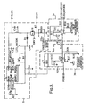
- exemplary circuit 20 provides control for an electrical device, for example, light-emitting diode (LED) 22, based on command signal 24.
- LED 22 may be a single LED or an array of LEDs, for example two series connected arrays of LEDs, or a video display screen having one or more matrices of LEDs.
- the term LED is defined to mean one or more LEDs.
- Exemplary circuit 20 includes linear current amplifier 26, voltage drop measurement amplifier 28, voltage shaping amplifier 30, and switching power supply 32; however, the invention also contemplates a circuit with a subset of these elements.
- command signal 24 may provide control for both current amplifier 26 and switching power supply 32, thereby controlling LED 22 without requiring voltage drop measurement amplifier 28 or voltage shaping amplifier 30.
- Current amplifier 26 advantageously provides linear control of current signal 34 flowing through LED 22.
- the remaining components of exemplary circuit 20 generally provide regulation of supply voltage signal 36 which is connected to and provides input to current amplifier 26 and LED 22.
- supply voltage signal 36 is regulated based on device voltage 38 measured across LED 22 and predetermined bias voltage 40 (Fig. 6).
- Supply voltage signal 36 is set to a level that supplies device voltage 38, the voltage drop across LED 22 occurring upon application of current signal 34, and the minimum voltage drop of current amplifier 26 which ensures linear operation, i.e. , current amplifier 26 components not in saturation. Regulating supply voltage signal 36 minimizes power dissipation of current amplifier 26.
- Voltage drop measurement amplifier 28 may be configured essentially as a differential amplifier and provides measurement of device voltage 38, the voltage drop across LED 22. Voltage-shaping amplifier 30 biases the measured device voltage 38 in order to provide bias voltage signal 62 for controlling switching power supply 32.
- command signal 24 may include the information of bias voltage signal 62, for example by including signal data based on calculated or experimentally determined voltage drop and bias voltage signals for the various input signals provided to current amplifier 26. By including such information with command signal 24, an alternative embodiment may not require voltage drop measurement amplifier 28 and/or voltage shaping amplifier 30.
- vehicle 42 includes exemplary imaging system 41 for determining the presence of occupant 44 in passenger compartment 46.
- imaging system 41 may include imaging control 48, imager 50, illumination control 52 and illumination device 54.
- Illumination device 54 may include, for example, LED 22 (Fig. 1).
- imaging control 48 provides an illumination intensity and duration to illumination control 52.
- Illumination control 52 provides command signal 24 (Fig. 1) to, for example, exemplary circuit 20 (Fig. 1).
- Illumination device 54 which includes, for example, LED 22, provides the specified illumination level and duration required for passenger compartment 46 so that imager 50 may capture an image for detection of occupant 44.
- exemplary circuit 20 portions of exemplary circuit 20 are shown, including exemplary schematic diagrams of switching power supply 32, voltage-shaping amplifier 30, and voltage drop measurement amplifier 28. Exemplary component values and part numbers for circuit 20 are listed in Table 1.
- Voltage drop measurement amplifier 28 measures device voltage 38, the voltage drop across LED 22, i.e. , between the anode and cathode.
- Voltage drop measurement amplifier 28 may be, for example, a differential amplifier having sufficient common mode accuracy and voltage range to measure the actual voltage drop of LED 22 as it is being driven by current amplifier 26.
- Exemplary voltage drop measurement amplifier 28 includes op amp U3 having a noninverting input coupled through resistor R14 to the anode of LED 22, and coupled to ground through resistor R15.
- the inverting input of op amp U3 is coupled through resistor R12 to the cathode of LED 22, and coupled to the output of op amp U3 through series resistor R11.
- the output of voltage drop measurement amplifier 28 provides device voltage signal 60 to the input of voltage-shaping amplifier 30.
- Voltage-shaping amplifier 30 receives device voltage signal 60 from voltage drop measurement amplifier 28 and includes predetermined bias voltage 40 (Fig. 6).
- Predetermined bias voltage 40 is set by the voltage divider circuit of R17 and R18 and is supplied to the noninverting input of op amp U4 in order to regulate supply voltage signal 36, regulated by power supply 32, to a higher voltage level than that determined by device voltage signal 60 alone.
- Device voltage signal 60 is received by the inverting input of op amp U4 through series resistor R13 and across resistor R16 to ground.
- the inverting input of op amp U4 is also coupled to the output of op amp U4 by parallel capacitor C7 and resistor R10.
- the output of op amp U4 provides biased voltage signal 62 which is connected to switching power supply 32.
- Voltage-shaping amplifier 30 of exemplary circuit 20 is configured as an inverting amplifier with predetermined bias voltage 40 (Fig. 6), which is coupled to the noninverting input of op amp U4, providing a positive bias that is overcome by device voltage signal 60 supplied to the inverting input of op amp U4.
- a minimum device voltage 60 of 16.74 volts results in a maximum bias voltage signal 62, provide to regulate power supply 32, of approximately 4.85 volts and a supply voltage signal 36 of approximately 18.1 volts.
- a maximum device voltage signal 60 of 35.63 volts results in a minimum bias voltage signal 62 of approximately 0.15 volts and a supply voltage signal 36 of approximately 37.9 volts.
- the exemplary voltage values of exemplary circuit 20 represent the range of operation for LED 22, two arrays of LEDs. For example at approximately 2.0 amperes, the voltage drop between the anodes to cathodes across the LEDs is approximately 35.9 volts, thus giving a desired supply voltage signal 36 of approximately 37.9 volts when taking into account the approximately 2 volts of voltage loss to associated components and represented by predetermined bias voltage 40.
- a supply voltage signal 36 of approximately 18.1 volts is the minimum for which power supply 32 can still boost and for which transistor Q2 is still dissipating an acceptable power level; however, at this level the current through LED 22 will typically be less than 100 milliamperes, which is below the useful operating range of LED 22.
- Switching power supply 32 of exemplary circuit 20 includes various components for regulating supply voltage signal 36, which is delivered to the anode of LED 22.
- Exemplary components include PWM switching regulator controller U1, which is operated in a current mode to provide linear voltage regulation; resistors R4 and R5 which determine voltage gain; resistor R6 which determines the maximum voltage of supply voltage signal 36; inductor L1, zener diode D1, capacitor C4, and transistor Q1 which modulate the current through inductor L1 and therefore regulate supply voltage signal 36 supplied to the anode of LED 22; resistor R7 which senses the current modulated through inductor L1 for regulation by controller U1; and compensation capacitors C1, C2, C4, C47, C48, and resistor R3 which keep switching power supply 32 stable. Modulating transistor Q1 is driven by output pin 6 of controller U1.
- Switching regulator controller U1 includes an internal reference voltage of approximately 1.25 volts at pin 3.
- the internal reference voltage is biased by bias voltage signal 62 provided through resistor R5 to regulate supply voltage signal 36 to the desired voltage level.
- the switching regulator controller U1 senses output voltage 36 of the supply via the feedback voltage at pin 3. It also senses the peak current flowing in inductor L1 using SEN, which measure across resistor R7 coupled to the source of transistor Q1. Controller U1 regulates the LED anode voltage by switching transistor Q1 on and off during the switching cycle interval. Transistor Q1 is switched on when the voltage at pin 3 is less than 1.25 volts except when the current exceeds the peak value determined by the SEN voltage, which is approximately 130 mV in the exemplary embodiment, and sense resistors R8 and R9.
- Transistor Q1 is turned on again at the next switching interval.
- transistor Q1 When transistor Q1 is turned off, the current in inductor L1 commutates, due to voltage fly-back of inductor L1, and current flows via diode D1 into output capacitor C4. A portion of the energy stored in inductor L1 is transferred to capacitor C4 in each switching cycle.
- Transistor Q1 is turned on again at the beginning of the next switching cycle.
- Switching regulator controller U1 actually varies the peak current sensed in response to the error voltage at pin 3 that in turn regulates output voltage 36 as a function of the LED current. To reduce LED current controller U1 effectively reduces the peak current sensed by its internal PWM mechanism. Current mode operation provides the most rapid transient response; however, implementation of current mode may vary with the vendor of switching controller IC. Alternatively, other switching controller ICs use the voltage mode alone and only the output voltage is sensed. Although exemplary circuit 20 utilizes current mode to regulate the voltage output, a voltage mode controller IC may be utilized, especial for continuous LED operation. Referring still to Fig. 3, switching power supply 32 is operated in an operational amplifier mode whereby the gain is determined by feedback resistor R4 over the voltage-shaping amplifier bias resistor R5.
- switching regulator controller U1 has an internal band gap reference of approximately 1.25 volts
- the operational gain of switching power supply 32 is equal to R4/R5.
- switching power supply 32 acts as an inverting operational amplifier with an offset voltage of approximately 1.25 volts at its differential input.
- Typical switching power supply PWM regulator chips are generally not used in this manner since a fixed output voltage is the common usage. Proper compensation of switching power supply 32 is therefore critical.
- exemplary circuit 20 utilizes a current mode switching power supply, circuit 20 is not restricted to this type.
- Exemplary current amplifier 26 operates as a voltage follower having sense resistor R30 coupled with the source of transistor Q2. The drain of transistor Q2 is connected to the cathode of LED 22. The current flow through LED 22 is measured across sense resistor R30.
- Op amp U6 is configured as a differential amplifier and provides a voltage feedback signal through resistor R26 to the inverting input of op amp U5.
- Op amp U5 compares the feedback voltage to command signal 24, which is received through resistors R34 and R28 at the noninverting input of op amp U5.
- Command signal 24 may be received from, for example imaging control 48 (Fig. 2).
- Command signal 24 may be provided by digital to analog converter (DAC) which converts a digital command signal to an analog voltage output, command signal 24.
- DAC digital to analog converter
- Capacitor C17 connected across the inverting input of op amp U5 and the output of op amp U5, slews until the inverting and noninverting inputs of op amp U5 are balanced, i.e., the point at which the desired current determined by command signal 24 is flowing through LED 22 and detected at resistor R30.
- the output of op amp U5 is coupled through resistor R27 to the gate of transistor Q2, thus regulating the flow of current through LED 22.
- Current amplifier 26 may be turned off by providing a high signal to the gate of transistor Q3, pulling the noninverting input of op amp U5 low, while the inverting input of op amp U5 is coupled through resistor R25 to a positive voltage supply, therefore turning transistor Q2 off and interrupting current flow through LED 22.
- the regulation of supply voltage signal provides voltage level to LED 22, and transistor Q2 and sense resistor R30, so that transistor Q2 may linearly control the current flow, i.e. , operate outside the saturation region, and dissipate minimal power.
- voltage supply 70 is a typical voltage regulation circuit which in exemplary circuit 20 provides Vcc of 5 volts.
- the upper saturation of op amp U4 is directly dependent on the accuracy of the 5 volt supply voltage.
- the upper saturation of op amp U4 affects the minimum LED anode supply voltage.
- FSYNC pin 1 is a particular feature of the controller IC selected for exemplary circuit 20.
- FSYNC allows the switching interval of the switching power supply IC to be controlled by an external frequency.
- Pin 7 of controller U1 is held low and the value of resistor R2 sets the frequency to approximately 300 kilohertz.
- SEN in conjunction with R8 and R9 in parallel, senses the peak current in the inductor L1.
- Bias voltage signal 62 which is connected from the output of op amp U4 to the gate of transistor Q2, is required to compensate for the drain capacitance of the drain of transistor Q2 because of the interaction of the dynamic voltage of power supply 32 and linear current amplifier 26.
- supply voltage signal 36 is a regulated voltage supplied by switching power supply 32 which is approximately equal to the sum of device voltage 38, i.e. , the voltage drop across LED 22, and the additional voltage required for linear operation of current amplifier 26.
- the additional voltage may be fixed, for example, predetermined bias voltage 40 in exemplary circuit 20 is approximately 2 volts.
- Predetermined bias voltage 40 is approximately equal to the minimal voltage across current amplifier 26, specifically, transistor Q2 and resistor R30. The value of predetermined bias voltage 40 ensures linear current regulation through transistor Q2 and includes an additional voltage to accommodate slew rate limitations of switching power supply 32 and the tolerance of feedback resistors and the 5 volt supply voltage.
- the combination of the band gap reference voltage, 5 volt supply voltage, and the resistors of Fig. 3 all contribute to the determination of output voltage 36.
- the resistors of voltage measurement amplifier 28 and the resistors directly connected to the feedback pin 3 of controller U1 significantly contribute to the determination of output voltage 36.
- R13 and R10 of voltage shaping amplifier 30 also contribute to the determination of output voltage 36.
- the sensitivity of these resistor tolerances varies as a function of the operating point on the curve shown in Fig. 6.
- the switching supply output 36 is defined by the internal band gap voltage of controller U1, the saturation voltages of op amp U4, and resistors R3, R4, and R6.
- resistors R11, R12, R14, R15, R13, R16, R17, R18, and R10 control the slope. Additionally, there is an interaction between the upper saturation voltage of U4 and the intercept defined by R16, R17 and R18. This intercept occurs at the saturation voltage of op amp U4 (approximately 4.85 volts) when the voltage across LED 22 equals approximately 16.0 volts. For voltages greater then 16.0 volts the output of op amp U4 decreases as the voltage drop across LED 22 increases. At the maximum LED voltage drop of approximately 36 volts, the lower saturation voltage of approximately 0.15 volts is reached and the LED anode voltage is maximum.
- Voltage-shaping amplifier 30 enables switching power supply 32 to provide power supply voltage signal 36 as shown in Fig. 6.
- Bias voltage signal 62 the output of voltage-shaping amplifier 30, saturates on both ends between ground and Vcc.
- Exemplary voltage-shaping amplifier 30 utilizes a rail to rail op amp U4.
- the two saturation levels of voltage-shaping amplifier 30 define the limits of the supply voltage signal 36.
- a maximum voltage of supply voltage signal 36 is set by the minimum output (ground) of voltage-shaping amplifier 30.
- the minimum output of supply voltage signal 36 is set by Vcc saturation of voltage-shaping amplifier 30.
- the two voltage limits of switching power supply 32 are set by the feedback ratio and bias voltage signal provided by voltage-shaping amplifier 30, as shown in Figs. 3 and 6.
- Bias voltage signal 40 embedded in the scaling of the voltage shaping amplifier 30 should command a voltage for supply voltage signal 36 which is slightly more voltage than is needed in order to avoid linear amplifier 26 from saturating and resulting in no current regulation.
- the voltage drop of linear amplifier 32 is regulated to approximately 2 volts (transistor Q2 drain voltage) for maximum current levels.
- Using precision resistor networks in voltage drop measurement amplifier 28, in voltage-shaping amplifier 30, and for feedback resistors R4, R5, and R6 of switching power supply 32 permits a lower predetermined bias voltage approaching the minimum voltage drop of transistor Q2, of approximately 0.5 volts.
- the accuracies of the internal band gap reference of switching regulator controller U2 and the 5 volt supply voltage remain limiting factors.
- peak power dissipation of linear amplifier 26 is approximately 2 volts multiplied by the commanded current totalling approximately 4 watts. If conventional unregulated power supply approaches are used, typical peak power dissipation of 20 watts or more results.
- Supply voltage signal 36 may be scaled.
- minimum voltage of supply voltage signal 36 is set by the minimum acceptable power dissipation of current amplifier 26 at low current operation. At this point, voltage of linear amplifier 26 equals the minimum voltage of supply voltage signal 36 provided by switching power supply 32.
- low current operation is less than approximately 0.1 amps, resulting in power dissipation of approximately 1.8 watts.
- the maximum voltage for supply voltage signal 36 is set by the maximum device voltage 38, the maximum voltage drop of LED 22 at maximum commanded current.
- maximum supply voltage signal 36 is approximately 38 volts for two arrays of LEDs in series and a commanded current of 2 amps.
- switching power supply 36 includes storage capacitor C4 which "parks" supply voltage signal 36 based on the last commanded voltage.
- parking supply voltage signal 36 at the last commanded voltage minimizes the rise time of supply voltage signal 36 and minimizes or eliminates the impact of the slew rates of switching power supply 32. Therefore, the power dissipation of linear amplifier 26 may be less than calculated above since linear amplifier 26 is initially saturated while settling to the current flow commanded by command signal 24.
- parking supply voltage signal 36 between periods of driving LED 22 prevents excessive peaking of the LED current because switching power supply 32 is initially unloaded and droops slightly when current amplifier 26 is again turned on. As a result, the initial current flow through LED 22 is very close to that commanded by command signal 24.
- an exemplary embodiment may include a microprocessor receiving command signal 24 and having software for determining output signals utilizing an analog to digital converter and digital to analog converters to drive a linear current amplifier and voltage supply regulator.
- Method 100 starts in step 102.
- a circuit voltage bias is determined.
- voltage-shaping amplifier 30 includes fixed predetermined bias voltage 40 which is determined as discussed above.
- an LED illumination level is specified, specifically command signal 24 is provided to current amplifier 26.
- step 108 the current flow through LED 22 which provides the specified illumination level is determined. Specifically, current amplifier 26 linearly regulates current flow through LED 22 based on command signal 24 received by DAC U7.
- step 110 the required current flow through LED 22 is set.
- current amplifier 26 measures the current flow through LED 22 at sense resistor R30 and uses a voltage follower configuration of op amps U5 and U6 and related components to regulate current flow at transistor Q2.
- step 112 the voltage drop across LED 22 is measured. Specifically, voltage drop measurement amplifier 28 measures the voltage difference between the cathode and anode of LED 22.
- step 114 the power supply voltage supplied to LED 22 is set. Specifically, switching power supply 32 receives bias voltage signal 62 from voltage-shaping amplifier 30 and voltage drop measurement amplifier 28 in order to linearly regulate supply voltage signal 36 provided to the anode of LED 22.
- step 116 method 100 is complete.
Landscapes
- Circuit Arrangement For Electric Light Sources In General (AREA)
- Led Devices (AREA)
- Arrangements Of Lighting Devices For Vehicle Interiors, Mounting And Supporting Thereof, Circuits Therefore (AREA)
- Lighting Device Outwards From Vehicle And Optical Signal (AREA)
Claims (9)
- Schaltung (20) zum Versorgen einer Vorrichtung (22) mit Leistung, wobei die Schaltung (20) umfasst:eine Leistungsversorgung (32), um für die Vorrichtung (22) ein Versorgungsspannungssignal (36) bereitzustellen;einen Stromverstärker (26), der so angeschlossen ist, dass er das Versorgungsspannungssignal (36) zu der Vorrichtung (22) mit einem gesteuerten Strom liefert, der in Abhängigkeit von einem Befehlssignal (24) linear reguliert wird;eine Spannungsmessvorrichtung (28), die geeignet ist, eine über der Vorrichtung (22) gemessene Vorrichtungsspannung (60) bereitzustellen;wobei das Versorgungsspannungssignal (36) durch die Leistungsversorgung (32) anhand der gemessenen Vorrichtungsspannung (60) reguliert wird, um die Verlustleistung im Stromverstärker minimal zu machen; dadurch gekennzeichnet, dassdie Vorrichtung (22) eine LED ist;die Schaltung ferner eine Vorspannungsschaltung (30) umfasst, die die Vorrichtungsspannung (60) empfängt und ein Vorspannungssignal (62) für einen Steuereingang (U1) der Leistungsversorgung (32) bereitstellt, wobei das Vorspannungssignal (62) durch die Vorspannungsschaltung (30) derart festgelegt wird, dass das Versorgungsspannungssignal (36) so reguliert wird, dass es angenähert gleich der Vorrichtungsspannung (60) zuzüglich einer vorgegebenen Vorspannung (40) ist.
- Schaltung nach Anspruch 1, bei der die vorgegebene Vorspannung (40) ungefähr anhand des minimalen Versorgungsspannungssignals (62), das bei dem maximalen Befehlssignal erforderlich ist, um eine Sättigung des Stromverstärkers (26) zu vermeiden, bestimmt wird, wodurch ein linearer Betrieb bei minimaler Verlustleistung geschaffen wird.
- Schaltung nach Anspruch 1, bei der der Stromverstärker (26) so beschaffen ist, dass er den Stromfluss durch die Vorrichtung (22) beendet, um dadurch die Vorrichtung (22) vorübergehend zu sperren.
- Schaltung nach Anspruch 3, bei der der Stromverstärker (26) einen Transistor (Q2) enthält, wovon wenigstens eine Source oder ein Drain mit der Vorrichtung (22) verbunden ist.
- Schaltung nach Anspruch 4, bei der der Stromverstärker (26) eine Stromerfassungsvorrichtung (R7) enthält, die mit der Vorrichtung (22) und/oder dem Transistor (Q2) gekoppelt ist; und der Stromverstärker einen Spannungsfolger (U5) enthält, der zwischen die Stromerfassungsvorrichtung (R7) und ein Gate des Transistors (Q2) geschaltet ist.
- Schaltung nach Anspruch 1, bei der die Leistungsversörgung (32) eine impulsbreitenmodulierte Schaltleistungsversorgung ist, die so konfiguriert ist, dass sie als linear einstellbare Spannungsversorgung arbeitet.
- Schaltung nach Anspruch 1, bei der die Vorspannungsschaltung (30) einen Differenzverstärker (U4) enthält, der die Vorrichtungsspannung und ein Signal (60) anhand der vorgegebenen Vorspannung empfängt.
- Schaltung nach einem vorhergehenden Anspruch, bei der das Befehlssignal (24) durch eine Steuereinheit (48) anhand eines gewünschten Beleuchtungspegels der Beleuchtungsquelle bereitgestellt wird.
- Verfahren zum Steuern einer Vorrichtung, das die folgenden Schritte umfasst:Bestimmen eines Beleuchtungspegels (106);Bestimmen des Stromflusses durch die Vorrichtung, der notwendig ist, um den Beleuchtungspegel (108) bereitzustellen;Begrenzen des Stromflusses durch die Vorrichtung auf den vorgegebenen Pegel (110);Bestimmen der Spannung über der Vorrichtung bei dem vorgegebenen Stromfluss (112);gekennzeichnet dadurch,dass die Vorrichtung eine LED ist; und durchBestimmen einer Vorspannung (104); undBereitstellen ungefähr der Summe aus der Vorspannung und der Spannung über der LED (114) für die LED.
Applications Claiming Priority (2)
| Application Number | Priority Date | Filing Date | Title |
|---|---|---|---|
| US753620 | 2004-01-08 | ||
| US10/753,620 US7038594B2 (en) | 2004-01-08 | 2004-01-08 | Led driver current amplifier |
Publications (2)
| Publication Number | Publication Date |
|---|---|
| EP1553808A1 EP1553808A1 (de) | 2005-07-13 |
| EP1553808B1 true EP1553808B1 (de) | 2007-11-28 |
Family
ID=34592580
Family Applications (1)
| Application Number | Title | Priority Date | Filing Date |
|---|---|---|---|
| EP04078514A Expired - Lifetime EP1553808B1 (de) | 2004-01-08 | 2004-12-23 | Stromverstärker für Leuchtdiodensteuerung |
Country Status (4)
| Country | Link |
|---|---|
| US (1) | US7038594B2 (de) |
| EP (1) | EP1553808B1 (de) |
| AT (1) | ATE379950T1 (de) |
| DE (1) | DE602004010359T2 (de) |
Families Citing this family (27)
| Publication number | Priority date | Publication date | Assignee | Title |
|---|---|---|---|---|
| US7635957B2 (en) * | 2003-09-04 | 2009-12-22 | Koninklijke Philips Electronics, N.V. | LED temperature-dependent power supply system and method |
| US7119498B2 (en) * | 2003-12-29 | 2006-10-10 | Texas Instruments Incorporated | Current control device for driving LED devices |
| DE102006000810B4 (de) * | 2006-01-03 | 2007-10-04 | Vossloh-Schwabe Optoelectronic Gmbh & Co. Kg | Verschaltete Anordnung von wenigstens einen Leuchtdiodenchip aufweisenden Einzelmodulen |
| TWI352949B (en) * | 2006-11-01 | 2011-11-21 | Chunghwa Picture Tubes Ltd | Light source driving circuit |
| TWI349902B (en) * | 2006-11-16 | 2011-10-01 | Chunghwa Picture Tubes Ltd | Controlling apparatuses for controlling a plurality of led strings and related light modules |
| US20080136227A1 (en) * | 2006-12-11 | 2008-06-12 | 3M Innovative Properties Company | Vehicle seat sensor assembly |
| US7911441B2 (en) * | 2006-12-25 | 2011-03-22 | Chunghwa Picture Tubes, Ltd. | Current-controlling apparatus for controlling current of light emitting diode string |
| WO2008096249A2 (en) * | 2007-02-07 | 2008-08-14 | Melexis Nv | Led driver |
| CN101675570B (zh) * | 2007-04-19 | 2013-07-31 | 高通股份有限公司 | 具有可调整电流限制的电池充电系统及方法 |
| US8903577B2 (en) | 2009-10-30 | 2014-12-02 | Lsi Industries, Inc. | Traction system for electrically powered vehicles |
| US8604709B2 (en) | 2007-07-31 | 2013-12-10 | Lsi Industries, Inc. | Methods and systems for controlling electrical power to DC loads |
| US7638950B1 (en) * | 2007-07-31 | 2009-12-29 | Lsi Industries, Inc. | Power line preconditioner for improved LED intensity control |
| US7598683B1 (en) | 2007-07-31 | 2009-10-06 | Lsi Industries, Inc. | Control of light intensity using pulses of a fixed duration and frequency |
| EP2225912B1 (de) * | 2007-12-20 | 2012-12-19 | Osram AG | Treiberanordnung für leuchtdioden |
| US8120277B2 (en) * | 2008-06-04 | 2012-02-21 | Boca Flasher, Inc. | Hybrid-control current driver for dimming and color mixing in display and illumination systems |
| DE102008040026A1 (de) * | 2008-06-30 | 2009-12-31 | Robert Bosch Gmbh | Schaltungsanordnung |
| TWI408643B (zh) * | 2008-09-18 | 2013-09-11 | Richtek Technology Corp | Led顯示系統及其控制方法以及該led顯示系統的驅動器及其控制方法 |
| CN101932168B (zh) * | 2009-06-25 | 2013-02-20 | 佛山普立华科技有限公司 | Led控制电路 |
| US20100329293A1 (en) * | 2009-06-26 | 2010-12-30 | Battelle Memorial Institute | Methods and Apparatus for Efficient, Low-noise, Precision Current Control |
| US20100327963A1 (en) * | 2009-06-26 | 2010-12-30 | Battelle Memorial Institute | Active Snubbers Providing Acceleration, Damping, and Error Correction |
| TWI422276B (zh) * | 2009-09-30 | 2014-01-01 | Lumens Digital Optics Inc | 發光二極體光源的投影機電力控制方法 |
| US8653760B1 (en) * | 2010-11-04 | 2014-02-18 | Tim C. Pearce | Electric tea light device |
| US9155139B2 (en) * | 2012-03-09 | 2015-10-06 | Rockwell Automation Technologies, Inc. | LED driver circuits and methods |
| US9307588B2 (en) * | 2012-12-17 | 2016-04-05 | Ecosense Lighting Inc. | Systems and methods for dimming of a light source |
| US9867242B1 (en) * | 2016-12-12 | 2018-01-09 | Datalogic Usa, Inc. | System and method of operating a constant current light-emitting diode pulsing drive circuit |
| US10483850B1 (en) | 2017-09-18 | 2019-11-19 | Ecosense Lighting Inc. | Universal input-voltage-compatible switched-mode power supply |
| US10816599B2 (en) * | 2019-01-16 | 2020-10-27 | International Business Machines Corporation | Dynamically power noise adaptive automatic test pattern generation |
Family Cites Families (8)
| Publication number | Priority date | Publication date | Assignee | Title |
|---|---|---|---|---|
| US3628102A (en) * | 1969-10-06 | 1971-12-14 | Ncr Co | Exciter apparatus for impact member solenoid |
| US5661645A (en) | 1996-06-27 | 1997-08-26 | Hochstein; Peter A. | Power supply for light emitting diode array |
| US6011360A (en) | 1997-02-13 | 2000-01-04 | Philips Electronics North America Corporation | High efficiency dimmable cold cathode fluorescent lamp ballast |
| CA2242720C (en) * | 1998-07-09 | 2000-05-16 | Ibm Canada Limited-Ibm Canada Limitee | Programmable led driver |
| US6198236B1 (en) | 1999-07-23 | 2001-03-06 | Linear Technology Corporation | Methods and apparatus for controlling the intensity of a fluorescent lamp |
| US6628252B2 (en) * | 2000-05-12 | 2003-09-30 | Rohm Co., Ltd. | LED drive circuit |
| US6621235B2 (en) | 2001-08-03 | 2003-09-16 | Koninklijke Philips Electronics N.V. | Integrated LED driving device with current sharing for multiple LED strings |
| US6690146B2 (en) | 2002-06-20 | 2004-02-10 | Fairchild Semiconductor Corporation | High efficiency LED driver |
-
2004
- 2004-01-08 US US10/753,620 patent/US7038594B2/en not_active Expired - Fee Related
- 2004-12-23 AT AT04078514T patent/ATE379950T1/de not_active IP Right Cessation
- 2004-12-23 EP EP04078514A patent/EP1553808B1/de not_active Expired - Lifetime
- 2004-12-23 DE DE602004010359T patent/DE602004010359T2/de not_active Expired - Lifetime
Also Published As
| Publication number | Publication date |
|---|---|
| US20050152123A1 (en) | 2005-07-14 |
| US7038594B2 (en) | 2006-05-02 |
| ATE379950T1 (de) | 2007-12-15 |
| DE602004010359T2 (de) | 2008-10-16 |
| EP1553808A1 (de) | 2005-07-13 |
| DE602004010359D1 (de) | 2008-01-10 |
Similar Documents
| Publication | Publication Date | Title |
|---|---|---|
| EP1553808B1 (de) | Stromverstärker für Leuchtdiodensteuerung | |
| US7423389B2 (en) | LED driving device of overvoltage protection and duty control | |
| US7622900B2 (en) | Semiconductor integrated circuit supplying voltage to a load using a charge pump and electronic device including the same | |
| US7402960B2 (en) | LED-based lamp apparatus | |
| US6628252B2 (en) | LED drive circuit | |
| US9526138B2 (en) | Load driving device, and lighting apparatus and liquid crystal display device using the same | |
| US7646184B2 (en) | Method and apparatus for maintaining a constant load current with line voltage in a switch mode power supply | |
| US7884558B2 (en) | Driver apparatus and method | |
| US8319449B2 (en) | Controlled voltage source for LED drivers | |
| US7705543B2 (en) | Supply device of circuit branches with LED diodes | |
| US7049879B2 (en) | Power supply circuit with control of rise characteristics of output voltage | |
| US7615974B1 (en) | High dimming ratio LED drive circuit | |
| US10405386B2 (en) | Light emitting element driving apparatus and driving method thereof | |
| CN101841954B (zh) | 用于控制负载的过程和电路 | |
| US20040251854A1 (en) | Power supply for lighting | |
| EP1643810A1 (de) | LED Ansteuerschaltung | |
| CN100414825C (zh) | 开关式电源电路以及随其配备的电子装置 | |
| US20060231745A1 (en) | Method and circuit arrangement for driving light-emitting diodes | |
| US20080309608A1 (en) | DC-DC converter with temperature compensation circuit | |
| US20080007322A1 (en) | Power supply apparatus | |
| US7781978B2 (en) | Vehicular lamp | |
| US8598919B2 (en) | Signal output circuit | |
| US20100052572A1 (en) | Light emitting element driving apparatus | |
| JP2018019025A (ja) | 電圧変換回路、led駆動回路及び電圧変換回路の制御方法 | |
| KR20070015857A (ko) | Led 구동 장치 |
Legal Events
| Date | Code | Title | Description |
|---|---|---|---|
| PUAI | Public reference made under article 153(3) epc to a published international application that has entered the european phase |
Free format text: ORIGINAL CODE: 0009012 |
|
| AK | Designated contracting states |
Kind code of ref document: A1 Designated state(s): AT BE BG CH CY CZ DE DK EE ES FI FR GB GR HU IE IS IT LI LT LU MC NL PL PT RO SE SI SK TR |
|
| AX | Request for extension of the european patent |
Extension state: AL BA HR LV MK YU |
|
| 17P | Request for examination filed |
Effective date: 20060113 |
|
| AKX | Designation fees paid |
Designated state(s): AT BE BG CH CY CZ DE DK EE ES FI FR GB GR HU IE IS IT LI LT LU MC NL PL PT RO SE SI SK TR |
|
| 17Q | First examination report despatched |
Effective date: 20060224 |
|
| GRAP | Despatch of communication of intention to grant a patent |
Free format text: ORIGINAL CODE: EPIDOSNIGR1 |
|
| GRAS | Grant fee paid |
Free format text: ORIGINAL CODE: EPIDOSNIGR3 |
|
| GRAA | (expected) grant |
Free format text: ORIGINAL CODE: 0009210 |
|
| AK | Designated contracting states |
Kind code of ref document: B1 Designated state(s): AT BE BG CH CY CZ DE DK EE ES FI FR GB GR HU IE IS IT LI LT LU MC NL PL PT RO SE SI SK TR |
|
| REG | Reference to a national code |
Ref country code: GB Ref legal event code: FG4D |
|
| REG | Reference to a national code |
Ref country code: IE Ref legal event code: FG4D |
|
| REG | Reference to a national code |
Ref country code: CH Ref legal event code: EP |
|
| REF | Corresponds to: |
Ref document number: 602004010359 Country of ref document: DE Date of ref document: 20080110 Kind code of ref document: P |
|
| PG25 | Lapsed in a contracting state [announced via postgrant information from national office to epo] |
Ref country code: SE Free format text: LAPSE BECAUSE OF FAILURE TO SUBMIT A TRANSLATION OF THE DESCRIPTION OR TO PAY THE FEE WITHIN THE PRESCRIBED TIME-LIMIT Effective date: 20080228 Ref country code: NL Free format text: LAPSE BECAUSE OF FAILURE TO SUBMIT A TRANSLATION OF THE DESCRIPTION OR TO PAY THE FEE WITHIN THE PRESCRIBED TIME-LIMIT Effective date: 20071128 Ref country code: LI Free format text: LAPSE BECAUSE OF FAILURE TO SUBMIT A TRANSLATION OF THE DESCRIPTION OR TO PAY THE FEE WITHIN THE PRESCRIBED TIME-LIMIT Effective date: 20071128 Ref country code: ES Free format text: LAPSE BECAUSE OF FAILURE TO SUBMIT A TRANSLATION OF THE DESCRIPTION OR TO PAY THE FEE WITHIN THE PRESCRIBED TIME-LIMIT Effective date: 20080311 Ref country code: CH Free format text: LAPSE BECAUSE OF FAILURE TO SUBMIT A TRANSLATION OF THE DESCRIPTION OR TO PAY THE FEE WITHIN THE PRESCRIBED TIME-LIMIT Effective date: 20071128 |
|
| NLV1 | Nl: lapsed or annulled due to failure to fulfill the requirements of art. 29p and 29m of the patents act | ||
| PG25 | Lapsed in a contracting state [announced via postgrant information from national office to epo] |
Ref country code: BG Free format text: LAPSE BECAUSE OF FAILURE TO SUBMIT A TRANSLATION OF THE DESCRIPTION OR TO PAY THE FEE WITHIN THE PRESCRIBED TIME-LIMIT Effective date: 20080228 Ref country code: PL Free format text: LAPSE BECAUSE OF FAILURE TO SUBMIT A TRANSLATION OF THE DESCRIPTION OR TO PAY THE FEE WITHIN THE PRESCRIBED TIME-LIMIT Effective date: 20071128 Ref country code: SI Free format text: LAPSE BECAUSE OF FAILURE TO SUBMIT A TRANSLATION OF THE DESCRIPTION OR TO PAY THE FEE WITHIN THE PRESCRIBED TIME-LIMIT Effective date: 20071128 Ref country code: LT Free format text: LAPSE BECAUSE OF FAILURE TO SUBMIT A TRANSLATION OF THE DESCRIPTION OR TO PAY THE FEE WITHIN THE PRESCRIBED TIME-LIMIT Effective date: 20071128 Ref country code: FI Free format text: LAPSE BECAUSE OF FAILURE TO SUBMIT A TRANSLATION OF THE DESCRIPTION OR TO PAY THE FEE WITHIN THE PRESCRIBED TIME-LIMIT Effective date: 20071128 Ref country code: IS Free format text: LAPSE BECAUSE OF FAILURE TO SUBMIT A TRANSLATION OF THE DESCRIPTION OR TO PAY THE FEE WITHIN THE PRESCRIBED TIME-LIMIT Effective date: 20080328 |
|
| REG | Reference to a national code |
Ref country code: CH Ref legal event code: PL |
|
| PG25 | Lapsed in a contracting state [announced via postgrant information from national office to epo] |
Ref country code: AT Free format text: LAPSE BECAUSE OF FAILURE TO SUBMIT A TRANSLATION OF THE DESCRIPTION OR TO PAY THE FEE WITHIN THE PRESCRIBED TIME-LIMIT Effective date: 20071128 |
|
| PG25 | Lapsed in a contracting state [announced via postgrant information from national office to epo] |
Ref country code: DK Free format text: LAPSE BECAUSE OF FAILURE TO SUBMIT A TRANSLATION OF THE DESCRIPTION OR TO PAY THE FEE WITHIN THE PRESCRIBED TIME-LIMIT Effective date: 20071128 Ref country code: MC Free format text: LAPSE BECAUSE OF NON-PAYMENT OF DUE FEES Effective date: 20071231 Ref country code: CZ Free format text: LAPSE BECAUSE OF FAILURE TO SUBMIT A TRANSLATION OF THE DESCRIPTION OR TO PAY THE FEE WITHIN THE PRESCRIBED TIME-LIMIT Effective date: 20071128 |
|
| PG25 | Lapsed in a contracting state [announced via postgrant information from national office to epo] |
Ref country code: RO Free format text: LAPSE BECAUSE OF FAILURE TO SUBMIT A TRANSLATION OF THE DESCRIPTION OR TO PAY THE FEE WITHIN THE PRESCRIBED TIME-LIMIT Effective date: 20071128 Ref country code: SK Free format text: LAPSE BECAUSE OF FAILURE TO SUBMIT A TRANSLATION OF THE DESCRIPTION OR TO PAY THE FEE WITHIN THE PRESCRIBED TIME-LIMIT Effective date: 20071128 Ref country code: BE Free format text: LAPSE BECAUSE OF FAILURE TO SUBMIT A TRANSLATION OF THE DESCRIPTION OR TO PAY THE FEE WITHIN THE PRESCRIBED TIME-LIMIT Effective date: 20071128 |
|
| EN | Fr: translation not filed | ||
| PG25 | Lapsed in a contracting state [announced via postgrant information from national office to epo] |
Ref country code: PT Free format text: LAPSE BECAUSE OF FAILURE TO SUBMIT A TRANSLATION OF THE DESCRIPTION OR TO PAY THE FEE WITHIN THE PRESCRIBED TIME-LIMIT Effective date: 20080428 |
|
| PLBE | No opposition filed within time limit |
Free format text: ORIGINAL CODE: 0009261 |
|
| STAA | Information on the status of an ep patent application or granted ep patent |
Free format text: STATUS: NO OPPOSITION FILED WITHIN TIME LIMIT |
|
| PG25 | Lapsed in a contracting state [announced via postgrant information from national office to epo] |
Ref country code: IE Free format text: LAPSE BECAUSE OF NON-PAYMENT OF DUE FEES Effective date: 20071224 Ref country code: FR Free format text: LAPSE BECAUSE OF FAILURE TO SUBMIT A TRANSLATION OF THE DESCRIPTION OR TO PAY THE FEE WITHIN THE PRESCRIBED TIME-LIMIT Effective date: 20080912 |
|
| 26N | No opposition filed |
Effective date: 20080829 |
|
| PG25 | Lapsed in a contracting state [announced via postgrant information from national office to epo] |
Ref country code: GR Free format text: LAPSE BECAUSE OF FAILURE TO SUBMIT A TRANSLATION OF THE DESCRIPTION OR TO PAY THE FEE WITHIN THE PRESCRIBED TIME-LIMIT Effective date: 20080229 Ref country code: EE Free format text: LAPSE BECAUSE OF FAILURE TO SUBMIT A TRANSLATION OF THE DESCRIPTION OR TO PAY THE FEE WITHIN THE PRESCRIBED TIME-LIMIT Effective date: 20071128 |
|
| PG25 | Lapsed in a contracting state [announced via postgrant information from national office to epo] |
Ref country code: CY Free format text: LAPSE BECAUSE OF FAILURE TO SUBMIT A TRANSLATION OF THE DESCRIPTION OR TO PAY THE FEE WITHIN THE PRESCRIBED TIME-LIMIT Effective date: 20071128 |
|
| GBPC | Gb: european patent ceased through non-payment of renewal fee |
Effective date: 20081223 |
|
| PG25 | Lapsed in a contracting state [announced via postgrant information from national office to epo] |
Ref country code: LU Free format text: LAPSE BECAUSE OF NON-PAYMENT OF DUE FEES Effective date: 20071223 |
|
| PG25 | Lapsed in a contracting state [announced via postgrant information from national office to epo] |
Ref country code: TR Free format text: LAPSE BECAUSE OF FAILURE TO SUBMIT A TRANSLATION OF THE DESCRIPTION OR TO PAY THE FEE WITHIN THE PRESCRIBED TIME-LIMIT Effective date: 20071128 Ref country code: HU Free format text: LAPSE BECAUSE OF FAILURE TO SUBMIT A TRANSLATION OF THE DESCRIPTION OR TO PAY THE FEE WITHIN THE PRESCRIBED TIME-LIMIT Effective date: 20080529 |
|
| PG25 | Lapsed in a contracting state [announced via postgrant information from national office to epo] |
Ref country code: GB Free format text: LAPSE BECAUSE OF NON-PAYMENT OF DUE FEES Effective date: 20081223 |
|
| PGFP | Annual fee paid to national office [announced via postgrant information from national office to epo] |
Ref country code: DE Payment date: 20091217 Year of fee payment: 6 |
|
| PG25 | Lapsed in a contracting state [announced via postgrant information from national office to epo] |
Ref country code: IT Free format text: LAPSE BECAUSE OF NON-PAYMENT OF DUE FEES Effective date: 20071231 |
|
| REG | Reference to a national code |
Ref country code: DE Ref legal event code: R119 Ref document number: 602004010359 Country of ref document: DE Effective date: 20110701 |
|
| PG25 | Lapsed in a contracting state [announced via postgrant information from national office to epo] |
Ref country code: DE Free format text: LAPSE BECAUSE OF NON-PAYMENT OF DUE FEES Effective date: 20110701 |