EP1554618B1 - Methode zur Herstellung eines Mikroresonators mit ultrahoher Güte aus Quarzglas auf Siliziumsubstrat - Google Patents
Methode zur Herstellung eines Mikroresonators mit ultrahoher Güte aus Quarzglas auf Siliziumsubstrat Download PDFInfo
- Publication number
- EP1554618B1 EP1554618B1 EP03816213A EP03816213A EP1554618B1 EP 1554618 B1 EP1554618 B1 EP 1554618B1 EP 03816213 A EP03816213 A EP 03816213A EP 03816213 A EP03816213 A EP 03816213A EP 1554618 B1 EP1554618 B1 EP 1554618B1
- Authority
- EP
- European Patent Office
- Prior art keywords
- micro
- cavity
- silica
- toroid
- disk
- Prior art date
- Legal status (The legal status is an assumption and is not a legal conclusion. Google has not performed a legal analysis and makes no representation as to the accuracy of the status listed.)
- Expired - Lifetime
Links
- 239000000758 substrate Substances 0.000 title claims abstract description 44
- VYPSYNLAJGMNEJ-UHFFFAOYSA-N Silicium dioxide Chemical compound O=[Si]=O VYPSYNLAJGMNEJ-UHFFFAOYSA-N 0.000 title claims description 182
- 239000000377 silicon dioxide Substances 0.000 title claims description 89
- 238000004519 manufacturing process Methods 0.000 title claims description 13
- XUIMIQQOPSSXEZ-UHFFFAOYSA-N Silicon Chemical compound [Si] XUIMIQQOPSSXEZ-UHFFFAOYSA-N 0.000 title abstract description 33
- 229910052710 silicon Inorganic materials 0.000 title abstract description 33
- 239000010703 silicon Substances 0.000 title abstract description 33
- 238000000034 method Methods 0.000 claims description 27
- 238000010438 heat treatment Methods 0.000 claims description 18
- BLIQUJLAJXRXSG-UHFFFAOYSA-N 1-benzyl-3-(trifluoromethyl)pyrrolidin-1-ium-3-carboxylate Chemical compound C1C(C(=O)O)(C(F)(F)F)CCN1CC1=CC=CC=C1 BLIQUJLAJXRXSG-UHFFFAOYSA-N 0.000 claims description 16
- 239000000463 material Substances 0.000 claims description 11
- 238000005530 etching Methods 0.000 claims description 6
- 230000007423 decrease Effects 0.000 claims description 2
- 230000003287 optical effect Effects 0.000 abstract description 23
- 239000000835 fiber Substances 0.000 description 16
- 238000012545 processing Methods 0.000 description 13
- 238000010168 coupling process Methods 0.000 description 9
- 230000005855 radiation Effects 0.000 description 9
- 230000008878 coupling Effects 0.000 description 8
- 238000005859 coupling reaction Methods 0.000 description 8
- 239000007789 gas Substances 0.000 description 8
- 238000005259 measurement Methods 0.000 description 7
- 239000011521 glass Substances 0.000 description 6
- 238000002844 melting Methods 0.000 description 6
- 230000008018 melting Effects 0.000 description 6
- 238000000576 coating method Methods 0.000 description 5
- 229910052691 Erbium Inorganic materials 0.000 description 4
- 239000011248 coating agent Substances 0.000 description 4
- UYAHIZSMUZPPFV-UHFFFAOYSA-N erbium Chemical compound [Er] UYAHIZSMUZPPFV-UHFFFAOYSA-N 0.000 description 4
- 230000010354 integration Effects 0.000 description 4
- 239000004005 microsphere Substances 0.000 description 4
- 235000012239 silicon dioxide Nutrition 0.000 description 4
- KRHYYFGTRYWZRS-UHFFFAOYSA-N Fluorane Chemical compound F KRHYYFGTRYWZRS-UHFFFAOYSA-N 0.000 description 3
- 230000005540 biological transmission Effects 0.000 description 3
- 238000000295 emission spectrum Methods 0.000 description 3
- 238000002474 experimental method Methods 0.000 description 3
- 238000004093 laser heating Methods 0.000 description 3
- 229920002120 photoresistant polymer Polymers 0.000 description 3
- 230000008569 process Effects 0.000 description 3
- 239000000126 substance Substances 0.000 description 3
- CSCPPACGZOOCGX-UHFFFAOYSA-N Acetone Chemical compound CC(C)=O CSCPPACGZOOCGX-UHFFFAOYSA-N 0.000 description 2
- 238000005253 cladding Methods 0.000 description 2
- 238000009826 distribution Methods 0.000 description 2
- 239000002019 doping agent Substances 0.000 description 2
- 230000005284 excitation Effects 0.000 description 2
- 230000005484 gravity Effects 0.000 description 2
- 238000012986 modification Methods 0.000 description 2
- 230000004048 modification Effects 0.000 description 2
- 239000013307 optical fiber Substances 0.000 description 2
- 238000010791 quenching Methods 0.000 description 2
- 239000004065 semiconductor Substances 0.000 description 2
- 230000003595 spectral effect Effects 0.000 description 2
- 238000012546 transfer Methods 0.000 description 2
- 238000000411 transmission spectrum Methods 0.000 description 2
- 101100043696 Drosophila melanogaster Stim gene Proteins 0.000 description 1
- 238000010521 absorption reaction Methods 0.000 description 1
- 230000004075 alteration Effects 0.000 description 1
- 238000013459 approach Methods 0.000 description 1
- 230000002238 attenuated effect Effects 0.000 description 1
- 229940088623 biologically active substance Drugs 0.000 description 1
- 230000008859 change Effects 0.000 description 1
- 239000003795 chemical substances by application Substances 0.000 description 1
- 230000000052 comparative effect Effects 0.000 description 1
- 238000011109 contamination Methods 0.000 description 1
- 230000001419 dependent effect Effects 0.000 description 1
- 238000013461 design Methods 0.000 description 1
- 238000010586 diagram Methods 0.000 description 1
- 230000009977 dual effect Effects 0.000 description 1
- 230000000694 effects Effects 0.000 description 1
- 230000005520 electrodynamics Effects 0.000 description 1
- 230000007613 environmental effect Effects 0.000 description 1
- 238000013213 extrapolation Methods 0.000 description 1
- 238000007306 functionalization reaction Methods 0.000 description 1
- 239000000156 glass melt Substances 0.000 description 1
- 229910000040 hydrogen fluoride Inorganic materials 0.000 description 1
- 238000005286 illumination Methods 0.000 description 1
- 230000001788 irregular Effects 0.000 description 1
- 238000002955 isolation Methods 0.000 description 1
- 238000001459 lithography Methods 0.000 description 1
- 239000000155 melt Substances 0.000 description 1
- 238000004377 microelectronic Methods 0.000 description 1
- 238000000206 photolithography Methods 0.000 description 1
- 238000005424 photoluminescence Methods 0.000 description 1
- 230000000644 propagated effect Effects 0.000 description 1
- 230000001902 propagating effect Effects 0.000 description 1
- 230000000171 quenching effect Effects 0.000 description 1
- 230000009467 reduction Effects 0.000 description 1
- 230000035945 sensitivity Effects 0.000 description 1
- 239000007787 solid Substances 0.000 description 1
- 238000001228 spectrum Methods 0.000 description 1
- 238000006467 substitution reaction Methods 0.000 description 1
- 239000000725 suspension Substances 0.000 description 1
- 230000007704 transition Effects 0.000 description 1
Images


Classifications
-
- G—PHYSICS
- G02—OPTICS
- G02B—OPTICAL ELEMENTS, SYSTEMS OR APPARATUS
- G02B6/00—Light guides; Structural details of arrangements comprising light guides and other optical elements, e.g. couplings
- G02B6/10—Light guides; Structural details of arrangements comprising light guides and other optical elements, e.g. couplings of the optical waveguide type
- G02B6/12—Light guides; Structural details of arrangements comprising light guides and other optical elements, e.g. couplings of the optical waveguide type of the integrated circuit kind
- G02B6/12007—Light guides; Structural details of arrangements comprising light guides and other optical elements, e.g. couplings of the optical waveguide type of the integrated circuit kind forming wavelength selective elements, e.g. multiplexer, demultiplexer
-
- H—ELECTRICITY
- H01—ELECTRIC ELEMENTS
- H01S—DEVICES USING THE PROCESS OF LIGHT AMPLIFICATION BY STIMULATED EMISSION OF RADIATION [LASER] TO AMPLIFY OR GENERATE LIGHT; DEVICES USING STIMULATED EMISSION OF ELECTROMAGNETIC RADIATION IN WAVE RANGES OTHER THAN OPTICAL
- H01S3/00—Lasers, i.e. devices using stimulated emission of electromagnetic radiation in the infrared, visible or ultraviolet wave range
- H01S3/05—Construction or shape of optical resonators; Accommodation of active medium therein; Shape of active medium
- H01S3/06—Construction or shape of active medium
- H01S3/0627—Construction or shape of active medium the resonator being monolithic, e.g. microlaser
-
- G—PHYSICS
- G02—OPTICS
- G02B—OPTICAL ELEMENTS, SYSTEMS OR APPARATUS
- G02B6/00—Light guides; Structural details of arrangements comprising light guides and other optical elements, e.g. couplings
- G02B6/24—Coupling light guides
- G02B6/26—Optical coupling means
- G02B6/28—Optical coupling means having data bus means, i.e. plural waveguides interconnected and providing an inherently bidirectional system by mixing and splitting signals
- G02B6/293—Optical coupling means having data bus means, i.e. plural waveguides interconnected and providing an inherently bidirectional system by mixing and splitting signals with wavelength selective means
- G02B6/29331—Optical coupling means having data bus means, i.e. plural waveguides interconnected and providing an inherently bidirectional system by mixing and splitting signals with wavelength selective means operating by evanescent wave coupling
- G02B6/29335—Evanescent coupling to a resonator cavity, i.e. between a waveguide mode and a resonant mode of the cavity
- G02B6/29338—Loop resonators
- G02B6/29343—Cascade of loop resonators
-
- H—ELECTRICITY
- H01—ELECTRIC ELEMENTS
- H01S—DEVICES USING THE PROCESS OF LIGHT AMPLIFICATION BY STIMULATED EMISSION OF RADIATION [LASER] TO AMPLIFY OR GENERATE LIGHT; DEVICES USING STIMULATED EMISSION OF ELECTROMAGNETIC RADIATION IN WAVE RANGES OTHER THAN OPTICAL
- H01S3/00—Lasers, i.e. devices using stimulated emission of electromagnetic radiation in the infrared, visible or ultraviolet wave range
- H01S3/05—Construction or shape of optical resonators; Accommodation of active medium therein; Shape of active medium
- H01S3/08—Construction or shape of optical resonators or components thereof
- H01S3/081—Construction or shape of optical resonators or components thereof comprising three or more reflectors
- H01S3/083—Ring lasers
-
- H—ELECTRICITY
- H01—ELECTRIC ELEMENTS
- H01S—DEVICES USING THE PROCESS OF LIGHT AMPLIFICATION BY STIMULATED EMISSION OF RADIATION [LASER] TO AMPLIFY OR GENERATE LIGHT; DEVICES USING STIMULATED EMISSION OF ELECTROMAGNETIC RADIATION IN WAVE RANGES OTHER THAN OPTICAL
- H01S5/00—Semiconductor lasers
- H01S5/10—Construction or shape of the optical resonator, e.g. extended or external cavity, coupled cavities, bent-guide, varying width, thickness or composition of the active region
- H01S5/1042—Optical microcavities, e.g. cavity dimensions comparable to the wavelength
-
- H—ELECTRICITY
- H01—ELECTRIC ELEMENTS
- H01S—DEVICES USING THE PROCESS OF LIGHT AMPLIFICATION BY STIMULATED EMISSION OF RADIATION [LASER] TO AMPLIFY OR GENERATE LIGHT; DEVICES USING STIMULATED EMISSION OF ELECTROMAGNETIC RADIATION IN WAVE RANGES OTHER THAN OPTICAL
- H01S5/00—Semiconductor lasers
- H01S5/10—Construction or shape of the optical resonator, e.g. extended or external cavity, coupled cavities, bent-guide, varying width, thickness or composition of the active region
- H01S5/1071—Ring-lasers
- H01S5/1075—Disk lasers with special modes, e.g. whispering gallery lasers
Definitions
- the present invention is directed to micro-cavity resonators, more particularly, ultra-high-Q micro-cavity resonators.
- micro-cavity resonators have been utilized to re-circulate light and store optical power.
- light traverses around an interior surface of the cavity.
- the optical power stored in the resonator can be used in cavity quantum electrodynamics (cQED), photonics, and various optics applications.
- the surface quality or finish usually affects how long light can re-circulate in the resonator.
- known high-Q micro-cavities include surface-tension induced micro-cavities (STIM), such as droplets or micro-spheres.
- STIM micro-spheres typically have smooth surfaces that allow light energy to be stored for longer periods of time and provide a high Q factor or Q value.
- the "Q factor” or "Q value” measures the stability of light within a resonator.
- the Q value measures the relationship between stored energy and the rate of dissipation of the energy.
- known STIMs or spherical micro-cavities can have Q factors that approach 10 billion, i.e., they can store light energy for 10 billion light cycles.
- Micro-cavities having higher Q factors can store light energy for longer periods of time compared to micro-cavities having lower Q factors.
- Micro-cavities with higher Q factors are also typically more sensitive compared to lower Q factor cavities.
- micro-cavities having higher Q factor values are generally preferred since they maintain light energy for longer periods of time and can be used in a broader range of applications.
- a "high" Q value is generally defined as a Q value up to about one million or 10 6
- an "ultra-high” Q value is generally defined as a Q value greater than a million.
- micro-cavity resonators capable of high or ultra-high Q values and the manner in which they are fabricated can be improved.
- the typical tradeoff between Q value and integration and control should be eliminated or mitigated.
- micro-resonators should be capable of "high” and “ultra” “high” Q values to "ultra high” Q values while, at the same time, being fabricated with traditional wafer-based processing techniques and equipment.
- micro-cavities capable of ultra-high Q values should be fabricated in a time and cost efficient manner with known wafer processing techniques.
- Ultra-high Q micro-resonators should also be of a form that is more easily adaptable and compatible with other planar circuits and standard microelectronics fabrication techniques for integration and production with each other.
- US-A-5343490 relates to a micro-resonator apparatus for the cavitation of electromagnetic energy, with cavitation being primarily dependent on whispering gallery mode energy.
- a method of fabricating a micro-cavity from a silica layer disposed upon a substrate characterized by the steps of: etching a silica disk from the silica layer; etching the substrate to form a pillar that supports the silica disk; and heating periphery portions of the silica disk to form a toroid-shaped silica micro-cavity supported by the pillar.
- the toroid-shaped silica micro cavity is a planar toroid-shaped silica micro-cavity.
- the toroid-shaped silica micro-cavity preferably has a Q value of at least 1.00 x 10 8 , and preferably between about 10 8 and 5 x 10 8 .
- the toroid-shaped silica micro-cavity has a diameter of at least about 10 micrometers and a Q value of about 500 million.
- the etching of the substrate to form the pillar is performed using a xenon difluoride (XeF2) gas.
- XeF2 gas isotropically etches the substrate so that portions of the substrate located below the toroid-shaped micro-cavity are removed from the pillar.
- the heating periphery portions comprise heating periphery portions of the silica disk so that the diameter of the silica disk decreases until molten silica material collapses to form the toroid-shaped micro-cavity. After which the diameter of the toroid-shaped micro-cavity is substantially constant.
- the heating periphery portions comprise heating periphery portions of the silica disk to form the toroid-shaped micro-cavity.
- the diameter of the toroid-shaped micro-cavity being limited by a size of a top surface of the pillar.
- the heating periphery portions comprise heating periphery portions with a CO 2 laser for about 1 microsecond to about 10 microseconds, preferably having a wavelength of about 10.6 micrometers.
- Embodiments of a micro-cavity resonator capable of ultra-high Q values and a method for fabricating an ultra-high Q micro-cavity resonator will now be described.
- the described micro-cavity and method provide ultra-high Q values that can be fabricated using known semiconductor and wafer processing techniques and equipment.
- the micro-cavities of the present invention can be fabricated in a time and cost effective manner and can also be integrated with other planar components and systems that are produced with planar fabrication techniques and equipment.
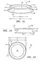
- an ultra-high Q micro-cavity assembly 100 includes an optical material or micro-cavity 110 and a substrate 120.
- the micro-cavity 110 is in the form of a ring, disk or toroid has a periphery or outer edge 112 and an inner edge 114.
- An outer diameter D1 is defined by the outer edges 114, and an inner diameter D2 is defined by the inner edges 112.
- the micro-cavity can be, for example, a silica micro-cavity.
- the substrate can be, for example, a silicon substrate.
- the substrate 120 includes a bottom surface 122, a middle tapered or angled surface 124, and a top surface 126. Portions of the silicon substrate 120 that are located below the micro-resonator 110, e.g., below a periphery 112 of the micro-resonator 110, are removed so that the substrate 120 is in a form of a support pillar. In the illustrated embodiment, the inner edge 114 of the micro-cavity extends around the outer edge of the top surface 126 of the substrate. Thus, the substrate 120 effectively supports and elevates the micro-cavity 110 above the bottom surface 122 of the substrate. In the illustrated embodiment, the ultra-high Q micro-cavity 110 is substantially parallel to a top surface 126 of the pillar.
- Optical energy travels along an inner surface of the outer edge 112 of the ultra-high Q micro-cavity 110, for example, within a whispering gallery mode (WGM) or other resonant modes as needed.
- WGM whispering gallery mode
- a WGM is a resonate mode in which optical energy electromagnetic waves are totally internally reflected, and focused by the inner surface of the micro-cavity.
- the optical energy can circulate within the micro-cavity and be confined therein to provide high and ultra-high Q values.
- the Q value of the micro-cavity resonation can influence different optical materials and surface finishes.
- Q values can also change based upon the diameter of the micro-cavity.
- the diameter of a silica micro-cavity can be from about 10 ⁇ m to about 500 ⁇ m, preferably between 15 ⁇ m to about 200 ⁇ m and the corresponding Q values can range from about 10 4 to about 10 9 .
- the ultra-high Q micro-cavity has a diameter of at least about 10 micrometers, e.g., between about 10 and about 30 micrometers, and a Q value of about 500 million.
- the size of the micro-cavity is one factor in providing an ultra-high Q value, and that the present invention is capable of supporting optical energy at various Q values including "high" Q values and even higher Q values, such as "ultra-high” Q values.
- the present invention is capable of achieving various ultra-high Q values, e.g., at least 10 6 or one million.
- the Q value may be about 10 8 or 100 million to about 5 x 10 8 or 500 million.
- micro-cavities having different shapes and sizes can have various ultra-high Q values.
- the micro-cavity 110 of the present invention is capable of providing both high and ultra-high Q values as previously defined.
- This specification refers to an ultra-high Q micro-cavity since micro-cavities having ultra-high Q values are generally preferred and may be utilized a broader range of applications.
- the invention is not so limited and can be utilized with both high and ultra-high Q experiments, applications and components.
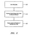
- FIG. 2 illustrates a method of fabricating an ultra-high Q micro-cavity according to the present invention.
- a silicon dioxide (SiO 2 ) disk or a circular pad is etched, for example, with a hydrogen fluoride (HF) solution.
- the silicon dioxide disk is exposed to a second etchant, such as xenon difluoride (XeF 2 ) gas, which removes portions of the silicon base beneath the periphery of the silicon dioxide disk.
- XeF 2 xenon difluoride
- Xenon difluoride is an etchant with high selectivity that is currently utilized to produce, for example, Micro Electrical Mechanical Systems (MEMS) devices.
- MEMS Micro Electrical Mechanical Systems
- a laser such as an Excimer or CO 2 laser
- the periphery portions of the disk are melted or partially or completely liquefied, and a toroid-shaped micro-cavity is formed, as shown in Figures 1A-C. It is believed that the molten silica collapses and adheres to itself due to the surface tension of silica.
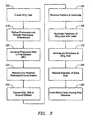
- Figure 3 illustrates further details of the method of fabricating a micro-cavity.
- an ultra-high Q silica micro-cavity is fabricated on a silicon substrate or wafer, preferably (100) prime grade silicon.
- the silicon substrate includes a thermal oxide layer having a thickness of, for example, about two micrometers or other suitable thicknesses as needed.
- step 300 known photolithography processing is used to create a disk-shaped photo-resist pad on the silicon substrate within an oxide layer (silica or SiO 2 disk).
- the SiO 2 disk can have a diameter of from about 10 ⁇ m to about 500 ⁇ m, preferably about 20 ⁇ m to about 200 ⁇ m, even more preferably about 160 ⁇ m.
- the photoresist can be heated again in step 310, if necessary, to reflow the photoresist and smooth the edges of the disk.
- the silica disk is immersed in a first etchant, e.g., a hydrogen fluoride (HF) etch solution at room temperature.
- a first etchant e.g., a hydrogen fluoride (HF) etch solution at room temperature.
- the silica disk acts as an etch mask when immersed in the HF solution.
- step 330 residual photoresist and any organic contamination can be removed with acetone or another suitable removal agent.
- the silica disk is exposed to a second etchant, e.g., xenon difluoride (XeF 2 ) gas at a pressure of about 3 Torr.
- a second etchant e.g., xenon difluoride (XeF 2 ) gas at a pressure of about 3 Torr.
- the silica disk acts as an etch mask during exposure to the XeF 2 gas.
- steps 350 portions of the silicon substrate are removed by the XeF 2 gas, and the remaining portions of the silicon substrate form a pillar, which supports the larger Silica disk above.
- the etchant used in step 340 is preferably a XeF 2 gas since it can selectively remove silicon.
- the XeF 2 gas isotropically removes silicon so that the periphery of the silica disk is equally undercut, leaving a tapered silicon pillar or substrate that supports the larger silica disk.
- the outer edges of the SiO 2 disk extend around the outer portion of the top surface of the silicon pillar. Removing the higher index silicon from the silicon substrate also serves to inhibit power leakage from the micro-resonator into the silicon substrate.
- WGMs whispering gallery modes
- the disk can have Q values exceeding 260,000.
- the Q value can reach levels of about 3.4 million.
- Q values of this magnitude within a resonant planar structure prepared on a silicon substrate may already surpass Q values of conventional planar resonators that are fabricated on the silicon substrates.
- the surface finish of the disk can be processed further to provide a smoother surface finish that can support substantially higher Q values, e.g., ultra-high Q values.
- the periphery of the silica disk can be melted and formed into a low loss, smooth surface, as described in the following steps 360-390.
- the periphery of the undercut silica disk is illuminated with a laser or other suitable radiation or heat source, such as a CO 2 laser that emits radiation at about 10.6 micrometers.
- a laser or other suitable radiation or heat source such as a CO 2 laser that emits radiation at about 10.6 micrometers.
- the intensity profile of the CO 2 beam preferably follows an approximate Gaussian distribution and is focused to a diameter of approximately 200 microns.
- CO 2 lasers are similar to lasers that are currently utilized in known before processing integrated circuit (IC) planarization.
- the intensity profile of the CO 2 beam preferably follows an approximate Gaussian distribution and is focused to a diameter of approximately 200 microns.
- the outer portions of the disk are sufficiently heated, in step 370, they melt or are partially or completely liquefied
- the molten silica overcomes the forces of gravity and adheres to itself so that the laser selectively reflows the undercut periphery of the silica disk.
- the CO 2 laser beam intensity can be varied as needed, but is typically about 100 MW/m 2 .
- step 380 as the molten silica disk is heated with the laser, the diameter of the disk structure becomes smaller which, in turn, reduces the effective cross-section of the disk that is available to absorb power from the laser.
- the molten silica shrinks and stabilizes into a toroid-like silica micro-cavity.
- the time required for the molten silica to assume the toroid-like shape can vary depending on, for example, the size of the disk and the amount and duration of laser radiation.
- the disk shrinks into the terminal toroid shape having a final diameter after laser radiation.
- laser heating may be utilized depending on the particular materials and micro-cavity applications, e.g., about 1 microsecond to about 10 seconds of laser heating may be utilized.
- the silicon pillar remains significantly cooler and physically unaffected throughout the silica reflow process, serving as a heat sink to selectively absorb and dissipate the heat generated by the reflow process. This is due to silicon having a weaker optical absorption than silica at 10.6 microns. Silicon is also about 100 times more thermally conductive than silica.
- the initial diameter of the SiO 2 disk can be, for example, from about 400 ⁇ m to about 1000 ⁇ m.
- the final or terminal outer diameter of the micro-cavity can be, for example, from about 10 ⁇ m to about 500 ⁇ m, preferably about 100 ⁇ m.
- the micro-cavity can have a thickness of about 1 ⁇ m to about 12 ⁇ m, preferably 4 ⁇ m.
- the final diameter of size of the micro-cavity can be limited by the size of the top surface of the silicon substrate. In other words, when needed the molten silica disk shrinks and collapses upon itself until the inner surface of the disk shrinks around the outer portion of the top surface of the silicon pillar. Thus, the micro-cavity is "self-quenching" when heated and assumes the shape of a toroid as a stable state.
- the final diameter of the micro-cavity can also be further controlled by additional lithography and chemical etch steps, as needed.
- the resulting toroid-shaped micro-cavity has smoother surfaces with an improved surface finish compared to the silica disk before the laser reflow processing.
- the toroid-shaped micro-cavity can have Q values exceeding one million (ultra-high Q values), whereas the Q value of the silica disk before the laser reflow processing was about 260,000 in this particular example.
- the surface finish of the toroid-shaped micro-cavity has a root mean square (rms) roughness of about several nanometers.
- rms root mean square
- These surface finishes are similar to surface finishes of micro-sphere resonators.
- the present invention unlike known micro-sphere resonators, provides these surface finishes and ultra-high Q values in a planar micro-resonator that can be prepared on a silicon substrate using known wafer processing and component integrating techniques.
- Other characteristics and technical aspects of an ultra-high Q micro-cavity resonator according to the present invention are described in " Ultra-High-Q Toroid Microcavity on a Chip," Nature, vol. 421, no. 6926, pp. 925-928 (February 27, 2003 ), the disclosure of which is incorporated herein by reference.
- the optical material may be a low melting point glass that has a melting point that is lower than silica, which has a melting point of about 1084°C ⁇ 38°C (1983°F ⁇ 100°F).
- Laser radiation can be applied to the low melting point glass to reflow the glass to form the micro-cavity.
- both the low melting point glass and the substrate e. g. silicon substrate
- the temperature is controlled so that the glass melts before the silicon substrate.
- the silicon substrates maintains its integrity, and the glass is melted into the ultra-high Q micro-cavity and can assume a toroid shape, as previously discussed.
- suitable materials besides silica and low melting point glass can be utilized if they possess a relatively high surface adhesion that can overcome forces of gravity.
- substrates besides a silicon substrate can be utilized, such as III-V substrates.
- the micro-cavityl 10 has a generally circular or disk shape.
- the micro-cavity shown in Figures A-C has a toroid or doughnut-like shape.
- Toroid dimensions may vary with the size of the micro-cavity.
- the toroid has a thickness of about five to about ten ⁇ m.
- micro-cavity resonators not according to the invention can have other shapes besides a disk or toroid-like shapes including, but not limited to, an elliptical shape, an oval or "race track”shape, partially toroid, elliptical, oval and circular shapes, and various other irregular shapes by utilizing different materials,etchants, heating/reflow temperatures, durations.
- This specification refers to and illustrates a toroid-shaped micro-cavity for purposes of explanation and illustration.
- the laser can be applied to different portions of the periphery of the SiO 2 disk for different periods of time and patterns for various degrees of reflow or to produce micro-cavities of different shapes.
- the laser can be applied to the silica disk so that it reflows and adheres to itself and consistently shrinks to its terminal diameter.
- the laser can also be applied to the silica disk for smaller amounts of time. In these instances, the diameter of the silica micro-resonator would be smaller than the initial diameter, but larger than the terminal diameter.
- the reflow process can be interrupted prior to quenching of the silica disk and forming a toroid shape.
- the micro-resonator would also have a smaller diameter than the terminal toroid diameter.
- the laser or other heat source can also be applied to selected sections of the silica disk for different amounts of time to produce micro-resonators with different shapes and sizes. As a result, only the heated sections may become smaller, thereby resulting in an elliptical or irregularly shaped micro-cavities. Accordingly, the above examples are merely illustrative of a prefered ultra-high Q micro-cavity. The invention, however is not so limited.
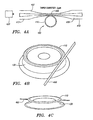
- transmission media 400 is utilized to carry optical energy stored in the micro-cavity. Active media, which are excited by optical pumps can also be associated with the micro-cavities to facilitate the lasing of a signal within a frequency band of interest.
- the transmission media 400 is a fiber waveguide, preferably a tapered waveguide as shown in Figure 4A, although other fiber configurations can also be utilized.
- the tapered sections 402 and 404 and the intermediate waist region 406 of the waveguide 400 may be provided, as is known, by stretching a fiber (e.g., a single mode fiber) under controllable tension as it is softened by one or more fixed or movable heat sources (e.g., torches).
- the ultra-high Q micro-cavity 100 is coupled to the externally guided power about the waist region 406 of the fiber 400.
- Taper waist 406 diameters are typically several microns, preferably about two microns. The diameter of the waist region can be adjusted to properly phase-match to the ultra-high Q micro-cavity resonator.
- Other discussions and details of such taper couplings can be found in United States Application No. 09/454,719 , entitled "Resonant Optical Wave Power Controlled Devices and Methods," filed December 7, 1999, the disclosure of which is incorporated by reference herein.
- the consequent reduction in diameter of about one or more orders of magnitude reduces the central core in the core/cladding structure of the optical fiber to vestigial size and function.
- the core no longer propagates a majority of the wave energy.
- the wave power in the full diameter fiber transitions into the waist region, where power is confined both within the attenuated cladding material and within a field emanating into the surrounding environment.
- exterior wave power is recaptured in the diverging tapered region and is again propagated with low loss within the outgoing fiber section 410.
- An optical pump 420 is optically connected to a first end 412 of the fiber.
- the optical pump 420 transmits a signal along the waveguide and to the ultra-high Q micro-cavity resonator through the fiber taper.
- One or more excited laser signals in the ultra-high Q micro-cavity resonator are then communicated to the fiber waveguide.
- the resonator recirculates the energy with low loss in, for example, a whispering gallery mode (WGM), or other resonant mode, returning a part of the power to the waveguide at the waist.
- WGM whispering gallery mode
- the ultra-high Q micro-cavity functions with effectively total internal reflection and with minimal internal attenuation and radiative losses.
- the mode structure and Q factor of toroid-shaped micro-cavities were characterized in an optical telecommunication band (1500 nm band).
- Tapered optical fibers (as previously discussed) were coupled to a single-mode, tunable, external-cavity laser to efficiently excite whispering gallery modes of the ultra-high Q micro-cavities.
- Tapered waveguides were positioned on a 20 nm resolution stage and could be moved freely over the sample to individually couple to each of the toroid-shaped micro-resonators. Dual microscopes were used to simultaneously image the micro-cavities and fiber tapers from the side and the top.
- the taper axis was adjusted to reside in the equatorial plane of the toroidal micro-cavity with minimal tilt angle.
- Critical coupling or the resonant transfer of all optical waveguide power into the resonator was achieved by adjusting the gap between the taper and the micro-cavity. Low non-resonant losses were observed (e.g., ⁇ 5%).
- Figures 5A and 5B illustrate graphs showing optical characteristics of two ultra-high Q micro-cavities according to the present invention.
- Figure 5A shows the transmission spectra through a taper in close proximity (on the order of hundreds of nanometers) to a 94 ⁇ m diameter toroidal micro-cavity according to the present invention.
- the observed free spectral range (FSR) corresponds to the equatorial mode number (1-index, which in this case is >270).
- the micro-cavity having a FSR of about 1 nm to about 100 nm.
- the micro-cavity also supports at least two azimuthal (m-index or transverse) modes.
- the micro-cavity can also be configured to have differential azimuthal modes of about 12 GHz.
- the micro-cavity can be configured to have a single radially and transversly supported mode.
- the Q factor of the micro-cavities was measured in two ways. First, the full-width half-maximum of the Lorentzian-shaped resonance in the undercoupled regime was directly measured by scanning a single-mode laser (short-term linewidth about 300 kHz) through a resonance. Low input power levels (typically less than 5 microwatts) were used to avoid thermally-induced distortion of the line shape due to resonant-field buildup within the cavity. Repeated measurements on samples fabricated with various radii (80-120 micron) and tori thickness (5-10 micron) yielded Q values in excess of 100 million (10 8 ), whereas previous known planar microresonators fabricated by wafer-scale processing typically have Q values as much as four orders of magnitude lower.
- a signal is applied to "gate" the laser off.
- the solid line represents an exponential fit as expected for decay of a single cavity mode.
- the inset shows a logarithmic plot to infer the cavity lifetime.
- the loaded lifetime in this structure was 43 ns.
- the silica ring can have a treated surface (such as a biotinlynated surface), a dopant or an embedded active optical component that may alter or functionalize the operation of an ultra-high Q micro-cavity resonator.
- the silica ring is doped with erbium.
- the silica ring includes an embedded active component, such as erbium.
- the ultra-high Q micro-cavity can also include a coating, such as a chemical or biologically active substance, to functionalize the micro-cavity surface.
- the ultra-high Q micro-cavity is coated with an doped sol-gel film 600, such as an erbium-doped sol-gel film.
- Sol-gel is a colloidal suspension of silica particles that is gelled to form a solid.
- Various commercially available sol-gel films can be doped with erbium.
- the Er+3 concentration in the sol-gel layer can be from about 0.1x10 16 to about 10 20 , preferably about 10 19 cm 3 .
- Other characteristics and technical aspects of a suitable sol-gel film are described in " Gain Functionalization of Silica Microresonators," Optics Letters, vol. 28, no. 8, pp. 592-594 (April 15, 2003 ), the disclosure of which is incorporated herein by reference.
- the silica micro-cavities are immersed in the sol-gel solution for about three to five hours, and then heated at about 160 °C for about 10 hours.
- the micro-cavities are then irradiated with a CO 2 laser, again at about 10.6 micrometers, in order to reflow and densify the sol-gel film.
- the sol-gel is selectively reflowed and densified at the periphery of the micro-cavity.
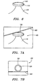
- a fiber-taper waveguide 700 can be coupled to the coated ultra-high Q micro-resonator, as previously described.
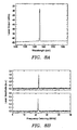
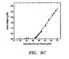
- Figures 8A-C illustrate the optical characteristics of a toroid micro-resonator that includes an erbium-doped sol gel coating prepared and applied according to the previously described method.
- Figure 8A is a graph that illustrates the emission spectrum of the sol-gel coated micro-resonator that is measured utilizing a high finesse scanning Fabry-Perot spectrometer.
- Figure 8B shows the spectra of a reference laser emission spectrum from a 1550 nm single mode laser with short term linewidth of 300 kHz and the emission of the erbium-doped sol-gel coated micro-cavity.
- Figure 8C illustrates the measured laser output versus the absorbed pump power for a micro-resonator having a diameter of about 80 micrometers.
- an ultra-high-Q planar micro-resonator can be fabricated on a chip, such as a silicon chip, or other suitable substrates.
- the combination of the planar configuration of the micro-cavity and ultra-high Q values enables these devices to be efficiently and consistently processed with know wafer processing techniques. Further, the large transparency window of silica enable these devices to be utilized in various photonics applications, as well as in fundamental studies. Doping and coating an ultra-high Q provides further enhancements. Electrical functionality can also be introduced to integrate control functions with the ultra-high-Q micro-cavities.
- the ultra-high Q micro-cavity can serve as atomic traps on a chip for chip-scale integration of cQED experiments and related devices.
- the ultra-high Q micro-resonators of the present invention are flexible and adaptable for use in various applications.
- the resonators can be used in telecommunications and environmental/chemical/biological sensing system, particularly sensing applications that require the high degree of sensitivity provided by the ultra-high Q micro-resonators of the present invention.
- references have been made in the foregoing description to various embodiments, persons of ordinary skill in the art will recognize that insubstantial modifications, alterations, and substitutions can be made to the described embodiments without departing from the invention as recited in the accompanying claims.
- Other substrates besides silicon may be suitable depending on the particular application of the device or integration and coupling considerations.
- sizes of ultra-high Q micro-cavities can be adjusted to use, and coatings and other devices can be used to functionalize the ultra-high Q micro-resonator.
Landscapes
- Physics & Mathematics (AREA)
- Optics & Photonics (AREA)
- Engineering & Computer Science (AREA)
- Electromagnetism (AREA)
- Plasma & Fusion (AREA)
- General Physics & Mathematics (AREA)
- Microelectronics & Electronic Packaging (AREA)
- Optical Integrated Circuits (AREA)
- Semiconductor Lasers (AREA)
- Control Of Motors That Do Not Use Commutators (AREA)
- Glass Compositions (AREA)
- Silicon Compounds (AREA)
- Crystals, And After-Treatments Of Crystals (AREA)
- Glass Melting And Manufacturing (AREA)
- Piezo-Electric Or Mechanical Vibrators, Or Delay Or Filter Circuits (AREA)
Claims (11)
- Verfahren zur Herstellung einer Mikrohohlraum-Baugruppe (100) aus einer Siliciumdioxidschicht, die auf einem Substrat angeordnet ist, gekennzeichnet durch die Sequenz der folgenden Schritte:Ätzen (200) einer Siliciumdioxidscheibe aus der Siliciumdioxidschicht;Ätzen (210) des Substrats zum Bilden einer Säule (120), die die Siliciumdioxidscheibe trägt; undErhitzen (220) von Peripherieabschnitten (112) der Siliciumdioxidscheibe zum Bilden eines ringförmigen Siliciumdioxid-Mikrohohlraums (110), der von der Säule (120) getragen wird.
- Verfahren nach Anspruch 1, wobei der ringförmige Siliciumdioxid-Mikrohohlraum (110) als planarer ringförmiger Siliciumdioxid-Mikrohohlraum ausgebildet ist.
- Verfahren nach Anspruch 1 oder 2, wobei der ringförmige Siliciumdioxid-Mikrohohlraum (110) einen Durchmesser von etwa 10 µm bis etwa 500 µm hat.
- Verfahren nach Anspruch 3, wobei der ringförmige Siliciumdioxid-Mikrohohlraum (110) einen Durchmesser von etwa 15 µm bis etwa 200 µm hat.
- Verfahren nach Anspruch 1 oder 2, wobei der ringförmige Siliciumdioxid-Mikrohohlraum (110) einen Durchmesser von etwa 10 µm bis etwa 30 µm hat.
- Verfahren nach einem der Ansprüche 1 bis 5, wobei der Schritt des Ätzens (210) des Substrats zum Bilden der Säule (120) mit einem Xenondifluorid-(XeF2)-gas ausgeführt wird.
- Verfahren nach Anspruch 6, wobei das Xenondifluorid-(XeF2)-gas zum isotropen Ätzen des Substrats verwendet wird, so dass Abschnitte des Substrats, die sich unterhalb des ringförmigen Mikrohohlraums (110) befinden, zum Bilden der Säule (120) entfernt werden.
- Verfahren nach einem der Ansprüche 1 bis 7, wobei der Schritt des Erhitzens (220) von Peripherieabschnitten (112) das Erhitzen von Peripherieabschnitten (112) der Siliciumdioxidscheibe beinhaltet, so dass der Durchmesser der Siliciumdioxidscheibe abnimmt, bis geschmolzenes Siliciumdioxidmaterial zusammenfällt und den ringförmigen Mikrohohlraum (110) bildet, wonach der Durchmesser des ringförmigen Mikrohohlraums (110) im Wesentlichen konstant ist.
- Verfahren nach einem der Ansprüche 1 bis 8, wobei der Schritt des Erhitzens (220) von Peripherieabschnitten (112) das Erhitzen von Peripherieabschnitten (112) der Siliciumdioxidscheibe beinhaltet, so dass die Siliciumdioxidscheibe schmilzt und schrumpft und auf sich selbst zusammenfällt, bis die Innenfläche der Siliciumdioxidscheibe um den äußeren Abschnitt einer Oberseite (126) der Säule (120) schrumpft, um dadurch den ringförmigen Mikrohohlraum (110) zu bilden.
- Verfahren nach einem der Ansprüche 1 bis 9, wobei der Schritt des Erhitzens (220) von Peripherieabschnitten (112) das Erhitzen der Peripherieabschnitte (112) mit einem CO2-Laser für eine Gesamtzeit von etwa 1 Mikrosekunde bis etwa 10 Sekunden beinhaltet.
- Verfahren nach Anspruch 10, wobei der Schritt des Erhitzens (220) von Peripherieabschnitten (112) das Erhitzen der Peripherieabschnitte (112) mit einem CO2-Laser mit einer Wellenlänge von etwa 10,6 Mikrometern beinhaltet.
Applications Claiming Priority (3)
| Application Number | Priority Date | Filing Date | Title |
|---|---|---|---|
| US41541202P | 2002-10-02 | 2002-10-02 | |
| US415412P | 2002-10-02 | ||
| PCT/US2003/031727 WO2004109351A2 (en) | 2002-10-02 | 2003-10-02 | Ultra-high q micro-resonator on silicon substrate and method of fabrication thereof |
Publications (2)
| Publication Number | Publication Date |
|---|---|
| EP1554618A2 EP1554618A2 (de) | 2005-07-20 |
| EP1554618B1 true EP1554618B1 (de) | 2007-09-12 |
Family
ID=33510284
Family Applications (1)
| Application Number | Title | Priority Date | Filing Date |
|---|---|---|---|
| EP03816213A Expired - Lifetime EP1554618B1 (de) | 2002-10-02 | 2003-10-02 | Methode zur Herstellung eines Mikroresonators mit ultrahoher Güte aus Quarzglas auf Siliziumsubstrat |
Country Status (6)
| Country | Link |
|---|---|
| US (1) | US7545843B2 (de) |
| EP (1) | EP1554618B1 (de) |
| AT (1) | ATE373250T1 (de) |
| AU (1) | AU2003304193A1 (de) |
| DE (1) | DE60316334T2 (de) |
| WO (1) | WO2004109351A2 (de) |
Families Citing this family (52)
| Publication number | Priority date | Publication date | Assignee | Title |
|---|---|---|---|---|
| US7781217B2 (en) * | 2002-10-02 | 2010-08-24 | California Institute Of Technology | Biological and chemical microcavity resonant sensors and methods of detecting molecules |
| US20050141809A1 (en) * | 2003-12-31 | 2005-06-30 | Gardner Donald S. | Microring and microdisk resonators for lasers fabricated on silicon wafers |
| US7769071B2 (en) * | 2004-02-02 | 2010-08-03 | California Institute Of Technology | Silica sol gel micro-laser on a substrate |
| US7515617B1 (en) | 2005-11-15 | 2009-04-07 | California Institute Of Technology | Photonic device having higher order harmonic emissions |
| US7515786B1 (en) * | 2006-07-21 | 2009-04-07 | The United States Of America As Represented By The Administrator Of The National Aeronautics And Space Administration | White-light whispering gallery mode optical resonator system and method |
| US7951299B2 (en) * | 2007-02-27 | 2011-05-31 | California Institute Of Technology | Method of fabricating a microresonator |
| US7793543B2 (en) * | 2007-05-04 | 2010-09-14 | Baker Hughes Incorporated | Method of measuring borehole gravitational acceleration |
| US20090067039A1 (en) * | 2007-09-07 | 2009-03-12 | Bernd Nebendahl | Optical micro resonator |
| US8107081B2 (en) | 2007-10-01 | 2012-01-31 | California Institute Of Technology | Micro-cavity gas and vapor sensors and detection methods |
| US8092855B2 (en) * | 2007-11-28 | 2012-01-10 | California Institute Of Technology | Click chemistry surface functionalization for resonant micro-cavity sensors |
| US9246529B2 (en) | 2008-01-25 | 2016-01-26 | California Institute Of Technology | Photonic RF down-converter based on optomechanical oscillation |
| US8102597B1 (en) * | 2008-05-15 | 2012-01-24 | Oewaves, Inc. | Structures and fabrication of whispering-gallery-mode resonators |
| US8593638B2 (en) * | 2008-10-02 | 2013-11-26 | California Institute Of Technology | Split frequency sensing methods and systems |
| US11754488B2 (en) | 2009-12-11 | 2023-09-12 | Washington University | Opto-mechanical system and method having chaos induced stochastic resonance and opto-mechanically mediated chaos transfer |
| WO2015050591A2 (en) * | 2013-06-12 | 2015-04-09 | Washington University | Tunable add-drop filter with an active resonator |
| US20150285728A1 (en) | 2009-12-11 | 2015-10-08 | Washington University | Detection of nano-scale particles with a self-referenced and self-heterodyned raman micro-laser |
| US8597577B2 (en) | 2010-02-19 | 2013-12-03 | California Institute Of Technology | Swept-frequency semiconductor laser coupled to microfabricated biomolecular sensor and methods related thereto |
| CN101957479B (zh) * | 2010-07-27 | 2011-10-05 | 中北大学 | 温度调制光学微腔耦合系统的输出方法及其耦合结构 |
| US9293887B2 (en) * | 2011-06-17 | 2016-03-22 | California Institute Of Technology | Chip-based laser resonator device for highly coherent laser generation |
| DE102011107360A1 (de) * | 2011-06-29 | 2013-01-03 | Karlsruher Institut für Technologie | Mikrooptisches Element, mikrooptisches Array und optisches Sensorensystem |
| US8361828B1 (en) * | 2011-08-31 | 2013-01-29 | Alta Devices, Inc. | Aligned frontside backside laser dicing of semiconductor films |
| US8399281B1 (en) * | 2011-08-31 | 2013-03-19 | Alta Devices, Inc. | Two beam backside laser dicing of semiconductor films |
| JP5871655B2 (ja) * | 2012-02-28 | 2016-03-01 | 学校法人慶應義塾 | シリカトロイド型光共振器の製造方法 |
| US8848760B2 (en) | 2012-06-06 | 2014-09-30 | California Institute Of Technology | On-chip optical reference cavity exhibiting reduced resonance center frequency fluctuations |
| CN102718180A (zh) * | 2012-06-28 | 2012-10-10 | 中国科学院苏州纳米技术与纳米仿生研究所 | 同心环芯纳米硅微盘微腔器件及其制备方法 |
| JP6066876B2 (ja) * | 2012-09-25 | 2017-01-25 | オーエフエス ファイテル,エルエルシー | 表面ナノスケール・アキシャル・フォトニックデバイスを製造する方法 |
| EP3097615B1 (de) | 2014-01-24 | 2020-03-11 | California Institute Of Technology | Stabilisierte mikrowellenfrequenzquelle |
| US9595918B2 (en) | 2014-03-06 | 2017-03-14 | California Institute Of Technology | Stable microwave-frequency source based on cascaded brillouin lasers |
| US9739770B2 (en) | 2014-03-14 | 2017-08-22 | California Institute Of Technology | Label-free detection of nanoparticles and biological molecules using microtoroid optical resonators |
| TWI603594B (zh) | 2014-09-19 | 2017-10-21 | 財團法人工業技術研究院 | 光通訊裝置和光通訊方法 |
| WO2016138291A1 (en) | 2015-02-26 | 2016-09-01 | California Institute Of Technology | Optical frequency divider based on an electro-optical-modulator frequency comb |
| CN104868351B (zh) * | 2015-04-27 | 2018-08-03 | 清华大学 | 一种调节回音壁模式微腔共振频率的方法 |
| CN105098575A (zh) * | 2015-07-22 | 2015-11-25 | 南京邮电大学 | 一种混合介质微腔全光调谐的窄带光纤激光器 |
| US10884189B2 (en) * | 2017-06-06 | 2021-01-05 | University Of Maryland, Baltimore County | Nanofiber-segment ring resonator |
| CN108321670B (zh) * | 2018-03-22 | 2023-12-01 | 华南理工大学 | 一种级联泵浦的微腔激光器 |
| CN112654915B (zh) * | 2018-07-25 | 2024-05-28 | 协同微波公司 | 使用单片集成多量子阱激光器和相位调制器的光电振荡器 |
| CN109638645B (zh) * | 2018-12-29 | 2021-04-06 | 中国科学院半导体研究所 | 可调谐耦合腔半导体激光器 |
| CN110289551B (zh) * | 2019-07-22 | 2020-09-15 | 中国科学院半导体研究所 | 用于激光显示的激光光源 |
| US10958040B1 (en) * | 2019-09-17 | 2021-03-23 | International Business Machines Corporation | Fabrication of ellipsoidal or semi-ellipsoidal semiconductor structures |
| US11081859B2 (en) * | 2019-09-30 | 2021-08-03 | Gm Cruise Holdings Llc | Optical resonator with localized ion-implanted voids |
| US11060869B2 (en) | 2019-11-27 | 2021-07-13 | Anello Photonics, Inc. | Ring waveguide based integrated photonics optical gyroscope with gain tuning for enhanced performance |
| CN110981168A (zh) * | 2019-12-03 | 2020-04-10 | 中国科学技术大学 | 一种超高品质因子回音壁模式微棒腔制备方法 |
| CA3158849A1 (en) | 2019-12-09 | 2021-06-17 | Lan Yang | Whispering gallery mode resonators for sensing applications |
| IL296907A (en) * | 2020-03-30 | 2022-12-01 | Deepsight Tech Inc | Optical microresonator array device for ultrasound sensing |
| JP7772723B2 (ja) | 2020-07-01 | 2025-11-18 | ディープサイト テクノロジー インコーポレイテッド | 光学センサを備えた音響光学ハーモニックイメージング |
| EP3985792B1 (de) * | 2020-10-13 | 2025-04-02 | IMEC vzw | Supraleitender resonator für quantenbits und dessen herstellung |
| CN113003531B (zh) * | 2021-02-08 | 2022-06-28 | 清华大学 | 一种实现频率调控的装置 |
| CN113507039B (zh) * | 2021-05-13 | 2022-07-08 | 华东师范大学 | 基于单个回音壁模式光学微腔的单模微激光器及实现方法 |
| CN113497401B (zh) * | 2021-06-25 | 2022-10-14 | 华中科技大学 | 一种稀土掺杂光学微腔及其制备方法 |
| US12416760B2 (en) | 2021-12-06 | 2025-09-16 | Oscps Motion Sensing Inc. | Low-loss photonic waveguides and ring resonators and a method for low-loss photonic waveguide and ring resonator fabrication |
| US12504580B2 (en) * | 2022-05-09 | 2025-12-23 | Intel Corporation | Reduced bridge structure for a photonic integrated circuit |
| US12320682B2 (en) | 2023-06-23 | 2025-06-03 | Washington University | High-Q whispering gallery mode (WGM) resonators encapsulated in polydimethylsilozane (PDMS) for highly sensitive displacement detection |
Family Cites Families (22)
| Publication number | Priority date | Publication date | Assignee | Title |
|---|---|---|---|---|
| US3589794A (en) | 1968-08-07 | 1971-06-29 | Bell Telephone Labor Inc | Optical circuits |
| US3760297A (en) | 1972-01-20 | 1973-09-18 | Int Standard Electric Corp | Laser to optical fiber coupling |
| GB1432949A (en) | 1972-08-25 | 1976-04-22 | Plessey Co Ltd | Silicon dioxide semiconductor product containing boron trioxide and phosphorus pentoxide dopants |
| US4282499A (en) | 1979-09-24 | 1981-08-04 | The United States Of America As Represented By The Secretary Of The Navy | Optically tunable resonant structure |
| US4695121A (en) | 1985-01-28 | 1987-09-22 | Polaroid Corporation | Integrated optic resonant structres and fabrication method |
| CA2068899C (en) * | 1991-09-17 | 1997-06-17 | Samuel Leverte Mccall | Whispering mode micro-resonator |
| JPH05203826A (ja) | 1992-01-29 | 1993-08-13 | Nippondenso Co Ltd | 光リングフィルタ |
| FR2703473B1 (fr) | 1993-03-31 | 1995-05-19 | Cit Alcatel | Filtre optique à résonateur en anneau. |
| US5878070A (en) | 1995-05-25 | 1999-03-02 | Northwestern University | Photonic wire microcavity light emitting devices |
| US5825799A (en) | 1995-05-25 | 1998-10-20 | Northwestern University | Microcavity semiconductor laser |
| US5651022A (en) | 1995-12-22 | 1997-07-22 | Atx Telecom Systems, Inc. | Multi-element monolithic solid state laser |
| IL119006A (en) | 1996-08-04 | 2001-04-30 | B G Negev Technologies And App | Optical filters with adjustable stay line |
| US5742633A (en) * | 1996-10-02 | 1998-04-21 | Yale University | Asymmetric resonant optical cavity apparatus |
| US6101300A (en) | 1997-06-09 | 2000-08-08 | Massachusetts Institute Of Technology | High efficiency channel drop filter with absorption induced on/off switching and modulation |
| US6052495A (en) | 1997-10-01 | 2000-04-18 | Massachusetts Institute Of Technology | Resonator modulators and wavelength routing switches |
| US6078605A (en) | 1998-02-20 | 2000-06-20 | Massachusetts Institute Of Technology | Track-changing utilizing phase response of resonators |
| AU2001247345A1 (en) * | 2000-03-09 | 2001-09-17 | California Institute Of Technology | Micro-cavity laser |
| AU2001250049A1 (en) * | 2000-03-22 | 2001-10-03 | California Institute Of Technology | Non-spherical whispering-gallery-mode microactivity |
| KR100355675B1 (ko) * | 2000-10-10 | 2002-10-11 | 한국과학기술원 | 표면감쇠파 미소공진기 레이저 |
| CN100550544C (zh) | 2000-11-28 | 2009-10-14 | 柔斯芒特股份有限公司 | 适用于测量物理和材料性能的光学传感器 |
| US20030021518A1 (en) | 2001-06-01 | 2003-01-30 | D-Wave Systems, Inc. | Optical transformer device |
| US20030179981A1 (en) | 2002-03-22 | 2003-09-25 | Lnl Technologies,Inc. | Tunable inorganic dielectric microresonators |
-
2003
- 2003-10-02 EP EP03816213A patent/EP1554618B1/de not_active Expired - Lifetime
- 2003-10-02 AT AT03816213T patent/ATE373250T1/de not_active IP Right Cessation
- 2003-10-02 AU AU2003304193A patent/AU2003304193A1/en not_active Abandoned
- 2003-10-02 WO PCT/US2003/031727 patent/WO2004109351A2/en not_active Ceased
- 2003-10-02 DE DE60316334T patent/DE60316334T2/de not_active Expired - Lifetime
- 2003-10-02 US US10/678,354 patent/US7545843B2/en not_active Expired - Lifetime
Also Published As
| Publication number | Publication date |
|---|---|
| ATE373250T1 (de) | 2007-09-15 |
| AU2003304193A1 (en) | 2005-01-04 |
| AU2003304193A8 (en) | 2005-01-04 |
| WO2004109351A3 (en) | 2005-05-26 |
| US7545843B2 (en) | 2009-06-09 |
| US20040179573A1 (en) | 2004-09-16 |
| EP1554618A2 (de) | 2005-07-20 |
| DE60316334T2 (de) | 2008-06-26 |
| DE60316334D1 (de) | 2007-10-25 |
| WO2004109351A2 (en) | 2004-12-16 |
Similar Documents
| Publication | Publication Date | Title |
|---|---|---|
| US7545843B2 (en) | Ultra-high Q micro-resonator and method of fabrication | |
| US20050163185A1 (en) | Surface functionalization of micro-resonators | |
| Liu et al. | On-chip erbium-doped lithium niobate microcavity laser | |
| CN113507039B (zh) | 基于单个回音壁模式光学微腔的单模微激光器及实现方法 | |
| US7781217B2 (en) | Biological and chemical microcavity resonant sensors and methods of detecting molecules | |
| Kippenberg et al. | Fabrication and coupling to planar high-Q silica disk microcavities | |
| Levi et al. | Directional light coupling from microdisk lasers | |
| US9042003B2 (en) | Chip-based frequency comb generator with microwave repetition rate | |
| US8818146B2 (en) | Silica-on-silicon waveguides and related fabrication methods | |
| US6507684B2 (en) | Optical microcavity resonator system | |
| US6741628B2 (en) | Micro-cavity laser | |
| US7528403B1 (en) | Hybrid silicon-on-insulator waveguide devices | |
| US7769071B2 (en) | Silica sol gel micro-laser on a substrate | |
| US20160190769A1 (en) | Chip-based laser resonator device for highly coherent laser generation | |
| US20050141809A1 (en) | Microring and microdisk resonators for lasers fabricated on silicon wafers | |
| WO2013184227A1 (en) | On-chip optical reference cavity exhibiting reduced resonance center frequency fluctuations | |
| Yan et al. | An erbium-doped whispering-gallery-mode microlaser for sensing | |
| Lin et al. | High-$ Q $ Si Microsphere Resonators Fabricated From Si-Cored Fibers for WGMs Excitation | |
| Bradley et al. | 1.8-µm thulium microlasers integrated on silicon | |
| Dorche et al. | High-quality factor tantalum pentoxide microring resonator mirror at 780 nm | |
| Zhang et al. | Whispering gallery mode based on-chip glass microbubble resonator for thermal sensing | |
| CN113410746B (zh) | 拉曼激光调制装置及方法 | |
| Boust et al. | Single-mode and multi-mode DBR lasers using InP-Si3N4/SiO2 integration | |
| Liu et al. | On-chip Lithium Niobate Heterogeneous Photonic Crystal Nanocavity Laser | |
| Marchena et al. | Whispering gallery modes at 800 nm and 1550 nm in concentric Si-nc/Er: SiO2 microdisks |
Legal Events
| Date | Code | Title | Description |
|---|---|---|---|
| PUAI | Public reference made under article 153(3) epc to a published international application that has entered the european phase |
Free format text: ORIGINAL CODE: 0009012 |
|
| 17P | Request for examination filed |
Effective date: 20050329 |
|
| AK | Designated contracting states |
Kind code of ref document: A2 Designated state(s): AT BE BG CH CY CZ DE DK EE ES FI FR GB GR HU IE IT LI LU MC NL PT RO SE SI SK TR |
|
| AX | Request for extension of the european patent |
Extension state: AL LT LV MK |
|
| DAX | Request for extension of the european patent (deleted) | ||
| 17Q | First examination report despatched |
Effective date: 20050729 |
|
| RIN1 | Information on inventor provided before grant (corrected) |
Inventor name: ARMANI, DENIZ, K. Inventor name: VAHALA, KERRY, J. Inventor name: SPILLANE, SEAN, M. Inventor name: KIPPENBERG, TOBIAS, J. |
|
| RIN1 | Information on inventor provided before grant (corrected) |
Inventor name: KIPPENBERG, TOBIAS, J. Inventor name: ARMANI, DENIZ, K. Inventor name: SPILLANE, SEAN, M. Inventor name: VAHALA, KERRY, J. |
|
| GRAP | Despatch of communication of intention to grant a patent |
Free format text: ORIGINAL CODE: EPIDOSNIGR1 |
|
| RIC1 | Information provided on ipc code assigned before grant |
Ipc: G02B 6/293 20060101AFI20070209BHEP |
|
| RTI1 | Title (correction) |
Free format text: METHOD OF FABRICATING A SILICA ULTRA-HIGH Q MICRO-RESONATOR ON SILICON SUBSTRATE |
|
| GRAS | Grant fee paid |
Free format text: ORIGINAL CODE: EPIDOSNIGR3 |
|
| GRAA | (expected) grant |
Free format text: ORIGINAL CODE: 0009210 |
|
| AK | Designated contracting states |
Kind code of ref document: B1 Designated state(s): AT BE BG CH CY CZ DE DK EE ES FI FR GB GR HU IE IT LI LU MC NL PT RO SE SI SK TR |
|
| REG | Reference to a national code |
Ref country code: GB Ref legal event code: FG4D |
|
| REG | Reference to a national code |
Ref country code: CH Ref legal event code: EP |
|
| REF | Corresponds to: |
Ref document number: 60316334 Country of ref document: DE Date of ref document: 20071025 Kind code of ref document: P |
|
| REG | Reference to a national code |
Ref country code: IE Ref legal event code: FG4D |
|
| PG25 | Lapsed in a contracting state [announced via postgrant information from national office to epo] |
Ref country code: FI Free format text: LAPSE BECAUSE OF FAILURE TO SUBMIT A TRANSLATION OF THE DESCRIPTION OR TO PAY THE FEE WITHIN THE PRESCRIBED TIME-LIMIT Effective date: 20070912 |
|
| PG25 | Lapsed in a contracting state [announced via postgrant information from national office to epo] |
Ref country code: AT Free format text: LAPSE BECAUSE OF FAILURE TO SUBMIT A TRANSLATION OF THE DESCRIPTION OR TO PAY THE FEE WITHIN THE PRESCRIBED TIME-LIMIT Effective date: 20070912 Ref country code: CH Free format text: LAPSE BECAUSE OF FAILURE TO SUBMIT A TRANSLATION OF THE DESCRIPTION OR TO PAY THE FEE WITHIN THE PRESCRIBED TIME-LIMIT Effective date: 20070912 Ref country code: LI Free format text: LAPSE BECAUSE OF FAILURE TO SUBMIT A TRANSLATION OF THE DESCRIPTION OR TO PAY THE FEE WITHIN THE PRESCRIBED TIME-LIMIT Effective date: 20070912 |
|
| NLV1 | Nl: lapsed or annulled due to failure to fulfill the requirements of art. 29p and 29m of the patents act | ||
| PG25 | Lapsed in a contracting state [announced via postgrant information from national office to epo] |
Ref country code: BE Free format text: LAPSE BECAUSE OF FAILURE TO SUBMIT A TRANSLATION OF THE DESCRIPTION OR TO PAY THE FEE WITHIN THE PRESCRIBED TIME-LIMIT Effective date: 20070912 |
|
| REG | Reference to a national code |
Ref country code: CH Ref legal event code: PL |
|
| PG25 | Lapsed in a contracting state [announced via postgrant information from national office to epo] |
Ref country code: ES Free format text: LAPSE BECAUSE OF FAILURE TO SUBMIT A TRANSLATION OF THE DESCRIPTION OR TO PAY THE FEE WITHIN THE PRESCRIBED TIME-LIMIT Effective date: 20071223 Ref country code: GR Free format text: LAPSE BECAUSE OF FAILURE TO SUBMIT A TRANSLATION OF THE DESCRIPTION OR TO PAY THE FEE WITHIN THE PRESCRIBED TIME-LIMIT Effective date: 20071213 Ref country code: NL Free format text: LAPSE BECAUSE OF FAILURE TO SUBMIT A TRANSLATION OF THE DESCRIPTION OR TO PAY THE FEE WITHIN THE PRESCRIBED TIME-LIMIT Effective date: 20070912 |
|
| ET | Fr: translation filed | ||
| PG25 | Lapsed in a contracting state [announced via postgrant information from national office to epo] |
Ref country code: CZ Free format text: LAPSE BECAUSE OF FAILURE TO SUBMIT A TRANSLATION OF THE DESCRIPTION OR TO PAY THE FEE WITHIN THE PRESCRIBED TIME-LIMIT Effective date: 20070912 Ref country code: PT Free format text: LAPSE BECAUSE OF FAILURE TO SUBMIT A TRANSLATION OF THE DESCRIPTION OR TO PAY THE FEE WITHIN THE PRESCRIBED TIME-LIMIT Effective date: 20080212 Ref country code: MC Free format text: LAPSE BECAUSE OF NON-PAYMENT OF DUE FEES Effective date: 20071031 Ref country code: SK Free format text: LAPSE BECAUSE OF FAILURE TO SUBMIT A TRANSLATION OF THE DESCRIPTION OR TO PAY THE FEE WITHIN THE PRESCRIBED TIME-LIMIT Effective date: 20070912 |
|
| PG25 | Lapsed in a contracting state [announced via postgrant information from national office to epo] |
Ref country code: SE Free format text: LAPSE BECAUSE OF FAILURE TO SUBMIT A TRANSLATION OF THE DESCRIPTION OR TO PAY THE FEE WITHIN THE PRESCRIBED TIME-LIMIT Effective date: 20071212 Ref country code: RO Free format text: LAPSE BECAUSE OF FAILURE TO SUBMIT A TRANSLATION OF THE DESCRIPTION OR TO PAY THE FEE WITHIN THE PRESCRIBED TIME-LIMIT Effective date: 20070912 |
|
| PLBE | No opposition filed within time limit |
Free format text: ORIGINAL CODE: 0009261 |
|
| STAA | Information on the status of an ep patent application or granted ep patent |
Free format text: STATUS: NO OPPOSITION FILED WITHIN TIME LIMIT |
|
| PG25 | Lapsed in a contracting state [announced via postgrant information from national office to epo] |
Ref country code: DK Free format text: LAPSE BECAUSE OF FAILURE TO SUBMIT A TRANSLATION OF THE DESCRIPTION OR TO PAY THE FEE WITHIN THE PRESCRIBED TIME-LIMIT Effective date: 20070912 |
|
| 26N | No opposition filed |
Effective date: 20080613 |
|
| PG25 | Lapsed in a contracting state [announced via postgrant information from national office to epo] |
Ref country code: IE Free format text: LAPSE BECAUSE OF NON-PAYMENT OF DUE FEES Effective date: 20071002 |
|
| PG25 | Lapsed in a contracting state [announced via postgrant information from national office to epo] |
Ref country code: EE Free format text: LAPSE BECAUSE OF FAILURE TO SUBMIT A TRANSLATION OF THE DESCRIPTION OR TO PAY THE FEE WITHIN THE PRESCRIBED TIME-LIMIT Effective date: 20070912 |
|
| PG25 | Lapsed in a contracting state [announced via postgrant information from national office to epo] |
Ref country code: SI Free format text: LAPSE BECAUSE OF FAILURE TO SUBMIT A TRANSLATION OF THE DESCRIPTION OR TO PAY THE FEE WITHIN THE PRESCRIBED TIME-LIMIT Effective date: 20070912 |
|
| PG25 | Lapsed in a contracting state [announced via postgrant information from national office to epo] |
Ref country code: CY Free format text: LAPSE BECAUSE OF FAILURE TO SUBMIT A TRANSLATION OF THE DESCRIPTION OR TO PAY THE FEE WITHIN THE PRESCRIBED TIME-LIMIT Effective date: 20070912 |
|
| PG25 | Lapsed in a contracting state [announced via postgrant information from national office to epo] |
Ref country code: LU Free format text: LAPSE BECAUSE OF NON-PAYMENT OF DUE FEES Effective date: 20071002 Ref country code: BG Free format text: LAPSE BECAUSE OF FAILURE TO SUBMIT A TRANSLATION OF THE DESCRIPTION OR TO PAY THE FEE WITHIN THE PRESCRIBED TIME-LIMIT Effective date: 20071212 |
|
| PG25 | Lapsed in a contracting state [announced via postgrant information from national office to epo] |
Ref country code: HU Free format text: LAPSE BECAUSE OF FAILURE TO SUBMIT A TRANSLATION OF THE DESCRIPTION OR TO PAY THE FEE WITHIN THE PRESCRIBED TIME-LIMIT Effective date: 20080313 Ref country code: TR Free format text: LAPSE BECAUSE OF FAILURE TO SUBMIT A TRANSLATION OF THE DESCRIPTION OR TO PAY THE FEE WITHIN THE PRESCRIBED TIME-LIMIT Effective date: 20070912 |
|
| PG25 | Lapsed in a contracting state [announced via postgrant information from national office to epo] |
Ref country code: IT Free format text: LAPSE BECAUSE OF NON-PAYMENT OF DUE FEES Effective date: 20071031 |
|
| REG | Reference to a national code |
Ref country code: FR Ref legal event code: PLFP Year of fee payment: 13 |
|
| PGFP | Annual fee paid to national office [announced via postgrant information from national office to epo] |
Ref country code: DE Payment date: 20151020 Year of fee payment: 13 Ref country code: GB Payment date: 20151020 Year of fee payment: 13 |
|
| PGFP | Annual fee paid to national office [announced via postgrant information from national office to epo] |
Ref country code: FR Payment date: 20150930 Year of fee payment: 13 |
|
| REG | Reference to a national code |
Ref country code: DE Ref legal event code: R119 Ref document number: 60316334 Country of ref document: DE |
|
| GBPC | Gb: european patent ceased through non-payment of renewal fee |
Effective date: 20161002 |
|
| REG | Reference to a national code |
Ref country code: FR Ref legal event code: ST Effective date: 20170630 |
|
| PG25 | Lapsed in a contracting state [announced via postgrant information from national office to epo] |
Ref country code: DE Free format text: LAPSE BECAUSE OF NON-PAYMENT OF DUE FEES Effective date: 20170503 Ref country code: FR Free format text: LAPSE BECAUSE OF NON-PAYMENT OF DUE FEES Effective date: 20161102 Ref country code: GB Free format text: LAPSE BECAUSE OF NON-PAYMENT OF DUE FEES Effective date: 20161002 |