EP1554777B1 - Antenne a materiau bip multi-faisceaux - Google Patents
Antenne a materiau bip multi-faisceaux Download PDFInfo
- Publication number
- EP1554777B1 EP1554777B1 EP03778447A EP03778447A EP1554777B1 EP 1554777 B1 EP1554777 B1 EP 1554777B1 EP 03778447 A EP03778447 A EP 03778447A EP 03778447 A EP03778447 A EP 03778447A EP 1554777 B1 EP1554777 B1 EP 1554777B1
- Authority
- EP
- European Patent Office
- Prior art keywords
- excitation
- radiating
- antenna
- radiant
- cavity
- Prior art date
- Legal status (The legal status is an assumption and is not a legal conclusion. Google has not performed a legal analysis and makes no representation as to the accuracy of the status listed.)
- Expired - Lifetime
Links
Images


Classifications
-
- H—ELECTRICITY
- H01—ELECTRIC ELEMENTS
- H01Q—ANTENNAS, i.e. RADIO AERIALS
- H01Q15/00—Devices for reflection, refraction, diffraction or polarisation of waves radiated from an antenna, e.g. quasi-optical devices
- H01Q15/0006—Devices acting selectively as reflecting surface, as diffracting or as refracting device, e.g. frequency filtering or angular spatial filtering devices
- H01Q15/006—Selective devices having photonic band gap materials or materials of which the material properties are frequency dependent, e.g. perforated substrates, high-impedance surfaces
-
- H—ELECTRICITY
- H01—ELECTRIC ELEMENTS
- H01Q—ANTENNAS, i.e. RADIO AERIALS
- H01Q19/00—Combinations of primary active antenna elements and units with secondary devices, e.g. with quasi-optical devices, for giving the antenna a desired directional characteristic
- H01Q19/10—Combinations of primary active antenna elements and units with secondary devices, e.g. with quasi-optical devices, for giving the antenna a desired directional characteristic using reflecting surfaces
- H01Q19/12—Combinations of primary active antenna elements and units with secondary devices, e.g. with quasi-optical devices, for giving the antenna a desired directional characteristic using reflecting surfaces wherein the surfaces are concave
- H01Q19/17—Combinations of primary active antenna elements and units with secondary devices, e.g. with quasi-optical devices, for giving the antenna a desired directional characteristic using reflecting surfaces wherein the surfaces are concave the primary radiating source comprising two or more radiating elements
-
- H—ELECTRICITY
- H01—ELECTRIC ELEMENTS
- H01Q—ANTENNAS, i.e. RADIO AERIALS
- H01Q25/00—Antennas or antenna systems providing at least two radiating patterns
- H01Q25/007—Antennas or antenna systems providing at least two radiating patterns using two or more primary active elements in the focal region of a focusing device
-
- H—ELECTRICITY
- H01—ELECTRIC ELEMENTS
- H01Q—ANTENNAS, i.e. RADIO AERIALS
- H01Q5/00—Arrangements for simultaneous operation of antennas on two or more different wavebands, e.g. dual-band or multi-band arrangements
-
- H—ELECTRICITY
- H01—ELECTRIC ELEMENTS
- H01Q—ANTENNAS, i.e. RADIO AERIALS
- H01Q5/00—Arrangements for simultaneous operation of antennas on two or more different wavebands, e.g. dual-band or multi-band arrangements
- H01Q5/20—Arrangements for simultaneous operation of antennas on two or more different wavebands, e.g. dual-band or multi-band arrangements characterised by the operating wavebands
- H01Q5/28—Arrangements for establishing polarisation or beam width over two or more different wavebands
Definitions
- Multi-beam antennas are widely used in space applications and especially in geostationary satellites to transmit to the earth's surface and / or receive information from the Earth's surface. They comprise for this purpose several radiating elements each generating a beam of electromagnetic waves spaced from the other beams. These radiating elements are, for example, placed near the focus of a parabola forming reflector of electromagnetic wave beams, the parabola and the multi-beam antenna being housed in a geostationary satellite. The parabola is intended to direct each beam on a corresponding area of the earth's surface. Each area of the Earth's surface illuminated by a beam of the multi-beam antenna is commonly referred to as a coverage area. Thus, each coverage area corresponds to a radiating element.
- each horn produces a substantially circular radiating spot forming the base of a conical beam radiated emission or reception.
- These horns are arranged next to each other so as to bring as close as possible the radiant spots of each other.
- FIG. 1A diagrammatically represents a multi-beam antenna with cornets in front view in which seven squares F1 to F7 indicate the bulk of seven cones arranged contiguously to one another. Seven circles S1 to S7, each inscribed in one of the squares F1 to F7, represent the radiating spots produced by the corresponding horns.
- the antenna of FIG. 1A is placed at the focus of a parabola of a geostationary satellite intended to transmit information on the French territory.
- Figure 1B shows areas C1 to C7 of coverage at -3 dB, each corresponding to a radiating spot of the antenna of Figure 1A.
- the center of each circle corresponds to a point on the earth's surface where the power received is maximum.
- the perimeter of each circle delimits an area within which the power received on the earth's surface is greater than half the maximum power received at the center of the circle.
- the radiating spots S1 to S7 are substantially contiguous, they produce cover areas at -3 dB disjoined from each other.
- the regions between the -3 dB coverage areas are referred to here as receiving holes.
- Each receiving hole therefore corresponds to a region of the earth's surface where the received power is less than half of the maximum power received. In these receiving holes, the received power may be insufficient for a receiver floor to function properly.
- FIG. 2A A partial front view of such a multi-beam antenna having a plurality of overlapping radiating spots is illustrated in Figure 2A.
- the radiating spot SR1 is formed from the SdR1 to SdR7 radiation sources arranged contiguously next to one another.
- a radiating spot SR2 is produced from SdR1, SdR2, SdR3 and SdR7 radiation sources and from SdR8 to SdR10 radiation sources.
- the SdR1 to SdR7 radiation sources are suitable for working at a first working frequency for creating a first substantially uniform electromagnetic wave beam at this first frequency.
- the sources of radiation SdR1 to SdR3 and SdR7 to SdR10 are adapted to work at a second working frequency so as to create a second electromagnetic wave beam, substantially uniform at this second working frequency.
- the sources of radiation SdR1 to SdR3 and SdR7 are able to work simultaneously at the first and second working frequencies.
- the first and second working frequencies are different from each other so as to limit interference between the first and second beams produced.
- radiation sources such as SdR1-3 radiation sources, are used both to create the SR1 radiating spot and the SR2 radiating spot, thereby producing an overlap of these two.
- An illustration of the arrangement of the -3 dB coverage areas created by a multi-beam antenna with overlapping radiating spots is shown in Figure 2B.
- Such an antenna can significantly reduce the receiving holes, or even make them disappear.
- this multi-beam antenna is more complex to order than conventional horn antennas.
- the aim of the invention is to remedy this drawback by proposing a simpler overlapping multi-beam antenna with radiating spots.
- each excitation element produces a single radiating spot forming the base or cross-section at the origin of an electromagnetic wave beam.
- this antenna is comparable with conventional horn antennas where a horn produces a single radiating spot.
- the control of this antenna is therefore similar to that of a conventional horn antenna.
- the excitation elements are placed so as to overlap the radiating spots. This antenna thus has the advantages of a multi-beam antenna with overlapping radiating spots without the complexity of the control of the excitation elements has been increased compared to that of multi-beam horn antennas.
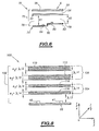
- FIG. 3 represents a multi-beam antenna 4.
- This antenna 4 is formed of a photonic ban band material or BIP material associated with a metallic plane 22 reflecting electromagnetic waves:
- the BIP materials are known and the design of a BIP material such as the material 20 is, for example, described in the patent application FR 99 14521. Thus, only the specific characteristics of the antenna 4 with respect to this state of the art. the technique will be described here in detail.
- a BIP material is a material which has the property of absorbing certain frequency ranges, that is to say of prohibiting any transmission in said aforementioned frequency ranges. These frequency ranges form what is called here a non-conducting band.
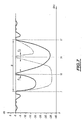
- FIG. 4 represents a curve representing the variations of the transmission coefficient expressed in decibels as a function of the frequency of the emitted or received electromagnetic wave: this transmission coefficient is representative of the energy transmitted on one side of the BIP material with respect to the energy received on the other side.
- the non-conducting band B or absorption band B extends substantially from 7 GHz to 17 GHz.
- This non-conducting band B depends solely on the properties and characteristics of the BIP material.
- the BIP material generally consists of a periodic arrangement of dielectric permittivity and / or variable permeability.
- the material 20 is formed from two blades 30, 32 made of a first magnetic material such as alumina and two blades 34 and 36 formed in a second magnetic material such as air.
- the blade 34 is interposed between the blades 30 and 32, while the blade 36 is interposed between the blade 32 and the reflector plane 22.
- the blade 30 is disposed at one end of this stack of blades. It has an outer surface 38 opposite its surface in contact with the blade 34. This surface 38 forms a radiating surface in emission and / or reception.
- the median frequency f m is substantially equal to 12 GHz.
- the radius R is substantially equal to 2.15 ⁇ .
- Such a parallelepiped resonant cavity has several families of resonant frequencies. Each family of resonance frequencies is formed by a fundamental frequency and its harmonics or integer multiples of the fundamental frequency. Each resonance frequency of the same family excites the same mode of resonance of the cavity. These resonance modes are known under the terms resonance modes TM 0 , TM 1 ,..., TM i , .... These modes of resonance are described in more detail in the document by F. Cardiol, "Electromagnetism, Electricity, Electronics and Electrical Engineering ", Ed. Dunod, 1987.
- each resonance mode corresponds to a radiation pattern of the particular antenna and to a radiating spot in emission and / or reception formed on the outer surface 38.
- the radiating spot is here the area of the outer surface 38 containing the entire points where the radiated power in emission and / or in reception is greater than or equal to half of the maximum power radiated from this external surface by the antenna 4.
- Each radiating spot has a geometrical center corresponding to the point where the power radiated is substantially equal to the maximum radiated power.
- this radiating spot is part of a circle whose diameter ⁇ is given by the formula (1).
- the radiation pattern is here highly directional along a direction perpendicular to the outer surface 38 and passing through the geometric center of the radiating spot.
- the radiation pattern corresponding to the TM 0 resonance mode is illustrated in FIG. 5.
- the frequencies f mi are placed inside the narrow bandwidth E.
- excitation elements 40 to 43 are placed next to one another in the cavity 36 on the reflector plane 22.
- the geometric centers of these excitation elements are placed at the four angles a rhombus whose dimensions of the sides are strictly smaller than 2R.
- Each of these excitation elements is able to emit and / or receive an electromagnetic wave at a working frequency f Ti different from that of the other excitation elements.
- the frequency f Ti of each excitation element is close to f mo so as to excite the resonance mode TM 0 of the cavity 36.
- These excitation elements 40 to 43 are connected to a conventional generator / receiver 45 of FIG. electrical signals to be transformed by each excitation element into an electromagnetic wave and vice versa.
- excitation elements are, for example, constituted by a radiating dipole, a radiating slot, a plate probe or a radiating patch.
- the lateral bulk of each radiating element that is to say in a plane parallel to the outer surface 38, is strictly smaller than the surface of the radiating spot to which it gives rise.
- the excitation element 40 In transmission, the excitation element 40, activated by the generator / receiver 45, emits an electromagnetic wave at a working frequency f T0 and excites the resonance mode TM 0 of the cavity 36.
- radiating elements 41 to 43 are, for example, simultaneously activated by the generator / receiver 45 and likewise respectively at the working frequencies f T1 , f T2 and f T3 .
- the radiating spot and the corresponding radiation pattern are independent of the lateral dimensions of the cavity 36.
- the resonance mode TM 0 is only a function of the thickness and the nature of the materials of each of the blades 30 to 36 and is established independently of the lateral dimensions of the cavity 36 when they are several times greater than the radius R defined above.
- several TM 0 resonance modes can be established simultaneously next to each other and thus simultaneously generate several radiating spots arranged next to each other. This is what happens when the excitation elements 40 to 43 excite, each at different points of space, the same mode of resonance.
- the excitation by the excitation element 40 of the resonance mode TM 0 results in the appearance of a radiant spot 46 that is substantially circular and whose geometric center is placed vertically above the geometric center of the element 40.
- excitation by the elements 41 to 43 of the TM 0 resonance mode results in the appearance, at the vertical of the geometric center of each of these elements, respectively of radiating spots 47 to 49.
- geometric center of the element 40 being at a distance strictly less than 2R of the geometric center of the elements 41 and 43, the radiating spot 46 partially overlaps the radiating spots 47 and 49 respectively corresponding to the radiating elements 41 and 43.
- the radiating spot 49 partially overlaps the radiating spots 46 and 48
- the radiating spot 48 partly overlaps the radiating spots 49 and 47
- the radiating spot 47 overlaps with the radiating spots 49 and 47 n part radiant spots 46 and 48.
- Each radiating spot corresponds to the base or cross section at the origin of a radiated electromagnetic wave beam.
- this antenna operates in a manner similar to the known overlapping multi-beam radiating beam antennas.
- the operation of the antenna in reception follows from that described in emission. So, for example, if an electromagnetic wave is emitted towards the radiating spot 46, it is received in the surface corresponding to the spot 46. If the received wave is at a frequency in the narrow bandwidth E, it is not absorbed by the BIP material 20 and is received by the excitation element 40. Each electromagnetic wave received by an excitation element is transmitted in the form of an electrical signal to the generator / receiver 45.
- FIG. 6 represents an antenna 70 made from a BIP material 72 and a reflector 74 of electromagnetic waves
- FIG. 7 shows the evolution of the transmission coefficient of this antenna as a function of frequency.
- the BIP material 72 is, for example, identical to the BIP material 20 and has the same non-conducting band B (FIG. 7).
- the blades forming this BIP material already described with reference to FIG. 3 bear the same numerical references.
- the reflector 74 is formed, for example, from the reflective plane 22 deformed so as to divide the cavity 36 into two resonant cavities 76 and 78 of different heights.
- the constant height H 1 of the cavity 76 is determined so as to place, within the non-conducting band B, a narrow bandwidth E 1 (FIG. 7), for example, around the frequency of 10 GHz.
- the height H 2 of the resonant cavity 78 is determined so as to place, within the same non-conducting band B, a narrow bandwidth E 2 (FIG. 7), for example centered around 14 GHz.
- the reflector 74 is composed here of two reflective half-planes 80 and 82 arranged in steps and electrically connected to one another.
- the reflective half-plane 80 is parallel to the blade 32 and spaced therefrom by the height H 1 .
- the half-plane 82 is parallel to the blade 32 and spaced therefrom from the constant height H 2 .
- an excitation element 84 is disposed in the cavity 76 and an excitation element 86 is disposed in the cavity 78.
- These excitation elements 84, 86 are, for example, identical to the excitation elements 40 to 43. with the exception that the excitation element 84 is able to excite the resonance mode TM 0 of the cavity 76, while the excitation element 86 is able to excite the resonance mode TM 0 of the cavity 78.
- the horizontal distance that is to say parallel to the blade 32, separating the geometric center of the elements of excitation 84 and 86, is strictly less than the sum of the radii of two radiating spots produced respectively by the elements 84 and 86.
- this antenna 70 is identical to that of the antenna of FIG. 3.
- the working frequencies of the excitation elements 84 and 86 are located in narrow bandwidths E 1 , E 2 respective. So; unlike the antenna 4 of FIG. 3, the working frequencies of each of these excitation elements are separated from each other by a large frequency interval, for example here 4 GHz.
- the positions of the pass bands E 1 , E 2 are chosen so as to be able to use imposed working frequencies.
- FIG. 8 represents a multi-beam antenna 100.
- This antenna 100 is similar to the antenna 4 except that the single-defective BIP material 20 of the radiating device 4 is replaced by a multi-fault BIP material 102.
- the elements already described with reference to FIG. 4 bear the same numerical references.
- the antenna 100 is shown in section along a section plane perpendicular to the reflector plane 22 and passing through the excitation elements 41 and 43.
- the BIP material 102 comprises two successive groups 104 and 106 of blades made of a first dielectric material.
- the groups 104 and 106 are superimposed in the direction perpendicular to the reflective plane 22.
- Each group 104, 106 is formed, by way of non-limiting example, respectively by two blades 110, 112 and 114, 116 parallel to the reflector plane 22.
- Each blade of a group has the same thickness as the other blades of this same grouping.
- each blade of the BIP 102 material is interposed a blade of a second dielectric material, such as air.
- the thickness of these blades separating the blades 110, 112, 114 and 116 is equal to ⁇ / 4.
- the first blade 116 is disposed vis-à-vis the reflector plane 22 and separated from this plane by a blade of second dielectric material thickness ⁇ / 2 so as to form a parallelepiped cavity resonant leak.
- the thickness e i of the blades of dielectric material, consecutive to each group of blades of dielectric material, is in geometric progression of reason q in the direction of successive groups 104, 106.
- the number of superimposed groups is equal to 2 so as not to overload the drawing, and the geometric progression reason is also taken equal to 2.
- This radiating device 100 derives directly from that of the antenna 4.
- each excitation element is polarized in a direction different from that used by the neighboring excitation elements.
- the polarization of each excitation element is orthogonal to that used by neighboring excitation elements.
- the same excitation element is adapted to operate successively or simultaneously at several different working frequencies.
- Such an element makes it possible to create a coverage area in which, for example, transmission and reception are done at wavelengths different.
- Such an excitation element is also able to make frequency switching.
Landscapes
- Physics & Mathematics (AREA)
- Optics & Photonics (AREA)
- Aerials With Secondary Devices (AREA)
- Variable-Direction Aerials And Aerial Arrays (AREA)
- Details Of Aerials (AREA)
- Waveguide Aerials (AREA)
Applications Claiming Priority (5)
| Application Number | Priority Date | Filing Date | Title |
|---|---|---|---|
| FR0213326A FR2854737A1 (fr) | 2002-10-24 | 2002-10-24 | Antenne a materiau bip multi-faisceaux et/ou multi- frequences et systeme mettant en oeuvre ces antennes. |
| FR0213326 | 2002-10-24 | ||
| FR0309473A FR2854735B1 (fr) | 2003-07-31 | 2003-07-31 | Antenne a materiau bip multi-faisceaux |
| FR0309473 | 2003-07-31 | ||
| PCT/FR2003/003147 WO2004040696A1 (fr) | 2002-10-24 | 2003-10-23 | Antenne a materiau bip multi-faisceaux |
Publications (2)
| Publication Number | Publication Date |
|---|---|
| EP1554777A1 EP1554777A1 (fr) | 2005-07-20 |
| EP1554777B1 true EP1554777B1 (fr) | 2006-05-03 |
Family
ID=32232268
Family Applications (1)
| Application Number | Title | Priority Date | Filing Date |
|---|---|---|---|
| EP03778447A Expired - Lifetime EP1554777B1 (fr) | 2002-10-24 | 2003-10-23 | Antenne a materiau bip multi-faisceaux |
Country Status (8)
| Country | Link |
|---|---|
| US (1) | US7242368B2 (es) |
| EP (1) | EP1554777B1 (es) |
| JP (1) | JP4181173B2 (es) |
| AT (1) | ATE325438T1 (es) |
| AU (1) | AU2003285446A1 (es) |
| DE (1) | DE60305056T2 (es) |
| ES (1) | ES2264018T3 (es) |
| WO (1) | WO2004040696A1 (es) |
Families Citing this family (14)
| Publication number | Priority date | Publication date | Assignee | Title |
|---|---|---|---|---|
| WO2004040695A1 (fr) * | 2002-10-24 | 2004-05-13 | Centre National De La Recherche Scientifique (C.N.R.S.) | Antenne a materiau bip multi-bandes de frequences |
| FR2906410B1 (fr) * | 2006-09-25 | 2008-12-05 | Cnes Epic | Antenne a materiau bip(bande interdite photonique), systeme et procede utilisant cette antenne |
| FR2914506B1 (fr) * | 2007-03-29 | 2010-09-17 | Centre Nat Rech Scient | Antenne a resonateur equipe d'un revetement filtrant et systeme incorporant cette antenne. |
| FR2939568B1 (fr) * | 2008-12-05 | 2010-12-17 | Thales Sa | Antenne a partage de sources et procede d'elaboration d'une antenne a partage de sources pour l'elaboration de multi-faisceaux |
| US8295788B2 (en) * | 2009-06-09 | 2012-10-23 | Broadcom Corporation | Method and system for an N-phase transmitter utilizing a leaky wave antenna |
| WO2012153164A1 (en) | 2011-05-06 | 2012-11-15 | Time Reversal Communications | A device for receiving and/or emitting a wave, a system comprising the device, and use of such device |
| EP2523256B1 (en) | 2011-05-13 | 2013-07-24 | Thomson Licensing | Multibeam antenna system |
| US9537208B2 (en) * | 2012-11-12 | 2017-01-03 | Raytheon Company | Dual polarization current loop radiator with integrated balun |
| US10270524B2 (en) * | 2014-04-15 | 2019-04-23 | Space Systems/Loral, Llc | Broadband satellite payload architecture |
| US10581177B2 (en) | 2016-12-15 | 2020-03-03 | Raytheon Company | High frequency polymer on metal radiator |
| US11088467B2 (en) | 2016-12-15 | 2021-08-10 | Raytheon Company | Printed wiring board with radiator and feed circuit |
| US10541461B2 (en) | 2016-12-16 | 2020-01-21 | Ratheon Company | Tile for an active electronically scanned array (AESA) |
| US10361485B2 (en) | 2017-08-04 | 2019-07-23 | Raytheon Company | Tripole current loop radiating element with integrated circularly polarized feed |
| US10424847B2 (en) | 2017-09-08 | 2019-09-24 | Raytheon Company | Wideband dual-polarized current loop antenna element |
Family Cites Families (8)
| Publication number | Priority date | Publication date | Assignee | Title |
|---|---|---|---|---|
| US4236161A (en) | 1978-09-18 | 1980-11-25 | Bell Telephone Laboratories, Incorporated | Array feed for offset satellite antenna |
| US6262830B1 (en) * | 1997-09-16 | 2001-07-17 | Michael Scalora | Transparent metallo-dielectric photonic band gap structure |
| FR2801428B1 (fr) | 1999-11-18 | 2004-10-15 | Centre Nat Rech Scient | Antenne pourvue d'un assemblage de materiaux filtrant |
| WO2003030298A1 (en) * | 2001-08-23 | 2003-04-10 | Broadcom Corporation | Apparatus for generating a magnetic interface and applications of the same |
| FR2830131B1 (fr) * | 2001-09-24 | 2005-06-24 | Centre Nat Rech Scient | Antenne a large bande ou multi-bandes |
| WO2004040695A1 (fr) * | 2002-10-24 | 2004-05-13 | Centre National De La Recherche Scientifique (C.N.R.S.) | Antenne a materiau bip multi-bandes de frequences |
| JP4181172B2 (ja) * | 2002-10-24 | 2008-11-12 | サントル ナシオナル ドゥ ラ ルシェルシェサイアンティフィク(セエヌエールエス) | フォトニックバンドギャップ材料によるマルチビームアンテナ |
| US7136028B2 (en) * | 2004-08-27 | 2006-11-14 | Freescale Semiconductor, Inc. | Applications of a high impedance surface |
-
2003
- 2003-10-23 AU AU2003285446A patent/AU2003285446A1/en not_active Abandoned
- 2003-10-23 AT AT03778447T patent/ATE325438T1/de not_active IP Right Cessation
- 2003-10-23 WO PCT/FR2003/003147 patent/WO2004040696A1/fr not_active Ceased
- 2003-10-23 DE DE60305056T patent/DE60305056T2/de not_active Expired - Lifetime
- 2003-10-23 EP EP03778447A patent/EP1554777B1/fr not_active Expired - Lifetime
- 2003-10-23 ES ES03778447T patent/ES2264018T3/es not_active Expired - Lifetime
- 2003-10-23 JP JP2005501825A patent/JP4181173B2/ja not_active Expired - Fee Related
- 2003-10-23 US US10/532,641 patent/US7242368B2/en not_active Expired - Lifetime
Also Published As
| Publication number | Publication date |
|---|---|
| JP2006504375A (ja) | 2006-02-02 |
| US7242368B2 (en) | 2007-07-10 |
| AU2003285446A8 (en) | 2004-05-25 |
| ES2264018T3 (es) | 2006-12-16 |
| JP4181173B2 (ja) | 2008-11-12 |
| DE60305056D1 (de) | 2006-06-08 |
| WO2004040696A1 (fr) | 2004-05-13 |
| ATE325438T1 (de) | 2006-06-15 |
| US20060132378A1 (en) | 2006-06-22 |
| AU2003285446A1 (en) | 2004-05-25 |
| DE60305056T2 (de) | 2006-12-07 |
| EP1554777A1 (fr) | 2005-07-20 |
Similar Documents
| Publication | Publication Date | Title |
|---|---|---|
| EP1568104B1 (fr) | Antenne multi-faisceaux a materiau bip | |
| EP1554777B1 (fr) | Antenne a materiau bip multi-faisceaux | |
| EP2795724B1 (fr) | Antenne élémentaire et antenne réseau mono ou bidimensionnelle correspondante | |
| EP2194602B1 (fr) | Antenne à partage de sources et procède d'élaboration d'une antenne à partage de sources pour l'élaboration de multi-faisceaux | |
| CA2243603C (fr) | Structure rayonnante | |
| CA2682273C (fr) | Antenne a resonateur equipe d'un revetement filtrant et systeme incorporant cette antenne | |
| EP1407512B1 (fr) | Antenne | |
| EP1416586B1 (fr) | Antenne pourvue d'un assemblage de matériaux filtrant | |
| EP0147325B1 (fr) | Antenne à deux réflecteurs cylindro-paraboliques croisés, et son procédé de fabrication | |
| FR2496347A1 (fr) | Antenne de systeme de navigation omnidirectionnelle a tres haute frequence | |
| FR2795240A1 (fr) | Antenne de station de base de radiocommunication | |
| EP3844844B1 (fr) | Antenne pour emettre et/ou recevoir une onde electromagnetique, et systeme comprenant cette antenne | |
| EP1554776A1 (fr) | Antenne a materiau bip multi-bandes de frequences | |
| FR2854737A1 (fr) | Antenne a materiau bip multi-faisceaux et/ou multi- frequences et systeme mettant en oeuvre ces antennes. | |
| EP0045254B1 (fr) | Source rayonnante bi-bande compacte fonctionnant dans le domaine des hyperfréquences | |
| CA2044903C (fr) | Antenne a balayage par variation de frequence | |
| FR2684809A1 (fr) | Antenne passive multifaisceaux a reflecteur(s) conforme (s). | |
| FR2854735A1 (fr) | Antenne a materiau bip multi-faisceaux | |
| CA2808511A1 (fr) | Antenne plane pour terminal fonctionnant en double polarisation circulaire, terminal aeroporte et systeme de telecommunication par satellite comportant au moins une telle antenne | |
| FR2854734A1 (fr) | Systeme d'emission et ou de reception d'ondes electromagnetiques equipe d'une antenne multi-faisceaux a materiau bip | |
| EP0088681B1 (fr) | Antenne à double réflecteur à transformateur de polarisation incorporé | |
| WO2001052356A1 (fr) | Antenne a cavite resonante ayant un faisceau conforme selon un diagramme de rayonnement predetermine | |
| FR2842025A1 (fr) | Dispositif rayonnant bi-bande a polarisations coplanaires | |
| FR2854738A1 (fr) | Antenne a materiau bip multi-bandes de frequences | |
| FR2814593A1 (fr) | Antenne de telecommunication, notamment entre avions |
Legal Events
| Date | Code | Title | Description |
|---|---|---|---|
| PUAI | Public reference made under article 153(3) epc to a published international application that has entered the european phase |
Free format text: ORIGINAL CODE: 0009012 |
|
| 17P | Request for examination filed |
Effective date: 20050408 |
|
| AK | Designated contracting states |
Kind code of ref document: A1 Designated state(s): AT BE BG CH CY CZ DE DK EE ES FI FR GB GR HU IE IT LI LU MC NL PT RO SE SI SK TR |
|
| GRAP | Despatch of communication of intention to grant a patent |
Free format text: ORIGINAL CODE: EPIDOSNIGR1 |
|
| GRAS | Grant fee paid |
Free format text: ORIGINAL CODE: EPIDOSNIGR3 |
|
| GRAA | (expected) grant |
Free format text: ORIGINAL CODE: 0009210 |
|
| AK | Designated contracting states |
Kind code of ref document: B1 Designated state(s): AT BE BG CH CY CZ DE DK EE ES FI FR GB GR HU IE IT LI LU MC NL PT RO SE SI SK TR |
|
| PG25 | Lapsed in a contracting state [announced via postgrant information from national office to epo] |
Ref country code: IT Free format text: LAPSE BECAUSE OF FAILURE TO SUBMIT A TRANSLATION OF THE DESCRIPTION OR TO PAY THE FEE WITHIN THE PRESCRIBED TIME-LIMIT;WARNING: LAPSES OF ITALIAN PATENTS WITH EFFECTIVE DATE BEFORE 2007 MAY HAVE OCCURRED AT ANY TIME BEFORE 2007. THE CORRECT EFFECTIVE DATE MAY BE DIFFERENT FROM THE ONE RECORDED. Effective date: 20060503 Ref country code: CZ Free format text: LAPSE BECAUSE OF FAILURE TO SUBMIT A TRANSLATION OF THE DESCRIPTION OR TO PAY THE FEE WITHIN THE PRESCRIBED TIME-LIMIT Effective date: 20060503 Ref country code: SK Free format text: LAPSE BECAUSE OF FAILURE TO SUBMIT A TRANSLATION OF THE DESCRIPTION OR TO PAY THE FEE WITHIN THE PRESCRIBED TIME-LIMIT Effective date: 20060503 Ref country code: FI Free format text: LAPSE BECAUSE OF FAILURE TO SUBMIT A TRANSLATION OF THE DESCRIPTION OR TO PAY THE FEE WITHIN THE PRESCRIBED TIME-LIMIT Effective date: 20060503 Ref country code: RO Free format text: LAPSE BECAUSE OF FAILURE TO SUBMIT A TRANSLATION OF THE DESCRIPTION OR TO PAY THE FEE WITHIN THE PRESCRIBED TIME-LIMIT Effective date: 20060503 Ref country code: SI Free format text: LAPSE BECAUSE OF FAILURE TO SUBMIT A TRANSLATION OF THE DESCRIPTION OR TO PAY THE FEE WITHIN THE PRESCRIBED TIME-LIMIT Effective date: 20060503 Ref country code: AT Free format text: LAPSE BECAUSE OF FAILURE TO SUBMIT A TRANSLATION OF THE DESCRIPTION OR TO PAY THE FEE WITHIN THE PRESCRIBED TIME-LIMIT Effective date: 20060503 Ref country code: IE Free format text: LAPSE BECAUSE OF FAILURE TO SUBMIT A TRANSLATION OF THE DESCRIPTION OR TO PAY THE FEE WITHIN THE PRESCRIBED TIME-LIMIT Effective date: 20060503 |
|
| REG | Reference to a national code |
Ref country code: GB Ref legal event code: FG4D Free format text: NOT ENGLISH |
|
| REG | Reference to a national code |
Ref country code: CH Ref legal event code: EP |
|
| REF | Corresponds to: |
Ref document number: 60305056 Country of ref document: DE Date of ref document: 20060608 Kind code of ref document: P |
|
| REG | Reference to a national code |
Ref country code: IE Ref legal event code: FG4D Free format text: LANGUAGE OF EP DOCUMENT: FRENCH |
|
| PG25 | Lapsed in a contracting state [announced via postgrant information from national office to epo] |
Ref country code: DK Free format text: LAPSE BECAUSE OF FAILURE TO SUBMIT A TRANSLATION OF THE DESCRIPTION OR TO PAY THE FEE WITHIN THE PRESCRIBED TIME-LIMIT Effective date: 20060803 |
|
| REG | Reference to a national code |
Ref country code: SE Ref legal event code: TRGR |
|
| GBT | Gb: translation of ep patent filed (gb section 77(6)(a)/1977) |
Effective date: 20060822 |
|
| PG25 | Lapsed in a contracting state [announced via postgrant information from national office to epo] |
Ref country code: PT Free format text: LAPSE BECAUSE OF FAILURE TO SUBMIT A TRANSLATION OF THE DESCRIPTION OR TO PAY THE FEE WITHIN THE PRESCRIBED TIME-LIMIT Effective date: 20061003 |
|
| PG25 | Lapsed in a contracting state [announced via postgrant information from national office to epo] |
Ref country code: MC Free format text: LAPSE BECAUSE OF NON-PAYMENT OF DUE FEES Effective date: 20061031 |
|
| REG | Reference to a national code |
Ref country code: ES Ref legal event code: FG2A Ref document number: 2264018 Country of ref document: ES Kind code of ref document: T3 |
|
| REG | Reference to a national code |
Ref country code: IE Ref legal event code: FD4D |
|
| PLBE | No opposition filed within time limit |
Free format text: ORIGINAL CODE: 0009261 |
|
| STAA | Information on the status of an ep patent application or granted ep patent |
Free format text: STATUS: NO OPPOSITION FILED WITHIN TIME LIMIT |
|
| 26N | No opposition filed |
Effective date: 20070206 |
|
| PG25 | Lapsed in a contracting state [announced via postgrant information from national office to epo] |
Ref country code: GR Free format text: LAPSE BECAUSE OF FAILURE TO SUBMIT A TRANSLATION OF THE DESCRIPTION OR TO PAY THE FEE WITHIN THE PRESCRIBED TIME-LIMIT Effective date: 20060804 |
|
| PG25 | Lapsed in a contracting state [announced via postgrant information from national office to epo] |
Ref country code: BG Free format text: LAPSE BECAUSE OF FAILURE TO SUBMIT A TRANSLATION OF THE DESCRIPTION OR TO PAY THE FEE WITHIN THE PRESCRIBED TIME-LIMIT Effective date: 20060803 Ref country code: EE Free format text: LAPSE BECAUSE OF FAILURE TO SUBMIT A TRANSLATION OF THE DESCRIPTION OR TO PAY THE FEE WITHIN THE PRESCRIBED TIME-LIMIT Effective date: 20060503 |
|
| PG25 | Lapsed in a contracting state [announced via postgrant information from national office to epo] |
Ref country code: TR Free format text: LAPSE BECAUSE OF FAILURE TO SUBMIT A TRANSLATION OF THE DESCRIPTION OR TO PAY THE FEE WITHIN THE PRESCRIBED TIME-LIMIT Effective date: 20060503 Ref country code: HU Free format text: LAPSE BECAUSE OF FAILURE TO SUBMIT A TRANSLATION OF THE DESCRIPTION OR TO PAY THE FEE WITHIN THE PRESCRIBED TIME-LIMIT Effective date: 20061104 |
|
| PG25 | Lapsed in a contracting state [announced via postgrant information from national office to epo] |
Ref country code: CY Free format text: LAPSE BECAUSE OF FAILURE TO SUBMIT A TRANSLATION OF THE DESCRIPTION OR TO PAY THE FEE WITHIN THE PRESCRIBED TIME-LIMIT Effective date: 20060503 |
|
| REG | Reference to a national code |
Ref country code: FR Ref legal event code: PLFP Year of fee payment: 14 |
|
| REG | Reference to a national code |
Ref country code: FR Ref legal event code: PLFP Year of fee payment: 15 |
|
| REG | Reference to a national code |
Ref country code: FR Ref legal event code: PLFP Year of fee payment: 16 |
|
| PGFP | Annual fee paid to national office [announced via postgrant information from national office to epo] |
Ref country code: LU Payment date: 20180913 Year of fee payment: 16 |
|
| PGFP | Annual fee paid to national office [announced via postgrant information from national office to epo] |
Ref country code: NL Payment date: 20180913 Year of fee payment: 16 |
|
| PGFP | Annual fee paid to national office [announced via postgrant information from national office to epo] |
Ref country code: DE Payment date: 20181009 Year of fee payment: 16 Ref country code: SE Payment date: 20181022 Year of fee payment: 16 |
|
| PGFP | Annual fee paid to national office [announced via postgrant information from national office to epo] |
Ref country code: CH Payment date: 20181022 Year of fee payment: 16 Ref country code: IT Payment date: 20181011 Year of fee payment: 16 Ref country code: ES Payment date: 20181126 Year of fee payment: 16 Ref country code: FR Payment date: 20181030 Year of fee payment: 16 Ref country code: GB Payment date: 20181017 Year of fee payment: 16 Ref country code: BE Payment date: 20181022 Year of fee payment: 16 |
|
| REG | Reference to a national code |
Ref country code: DE Ref legal event code: R119 Ref document number: 60305056 Country of ref document: DE |
|
| REG | Reference to a national code |
Ref country code: CH Ref legal event code: PL |
|
| REG | Reference to a national code |
Ref country code: NL Ref legal event code: MM Effective date: 20191101 |
|
| PG25 | Lapsed in a contracting state [announced via postgrant information from national office to epo] |
Ref country code: LU Free format text: LAPSE BECAUSE OF NON-PAYMENT OF DUE FEES Effective date: 20191023 Ref country code: CH Free format text: LAPSE BECAUSE OF NON-PAYMENT OF DUE FEES Effective date: 20191031 Ref country code: DE Free format text: LAPSE BECAUSE OF NON-PAYMENT OF DUE FEES Effective date: 20200501 Ref country code: LI Free format text: LAPSE BECAUSE OF NON-PAYMENT OF DUE FEES Effective date: 20191031 |
|
| REG | Reference to a national code |
Ref country code: BE Ref legal event code: MM Effective date: 20191031 |
|
| PG25 | Lapsed in a contracting state [announced via postgrant information from national office to epo] |
Ref country code: SE Free format text: LAPSE BECAUSE OF NON-PAYMENT OF DUE FEES Effective date: 20191024 Ref country code: BE Free format text: LAPSE BECAUSE OF NON-PAYMENT OF DUE FEES Effective date: 20191031 Ref country code: NL Free format text: LAPSE BECAUSE OF NON-PAYMENT OF DUE FEES Effective date: 20191101 |
|
| GBPC | Gb: european patent ceased through non-payment of renewal fee |
Effective date: 20191023 |
|
| PG25 | Lapsed in a contracting state [announced via postgrant information from national office to epo] |
Ref country code: FR Free format text: LAPSE BECAUSE OF NON-PAYMENT OF DUE FEES Effective date: 20191031 Ref country code: GB Free format text: LAPSE BECAUSE OF NON-PAYMENT OF DUE FEES Effective date: 20191023 Ref country code: IT Free format text: LAPSE BECAUSE OF NON-PAYMENT OF DUE FEES Effective date: 20191023 |
|
| PG25 | Lapsed in a contracting state [announced via postgrant information from national office to epo] |
Ref country code: ES Free format text: LAPSE BECAUSE OF NON-PAYMENT OF DUE FEES Effective date: 20191024 |